

现货库存、技术资料、百科信息、热点资讯,精彩尽在鼎好!
CA139, CA139A, CA239, CA339,
LM339, LM2901, LM3302
Data Sheet October 1999
Quad Voltage Comparators for Industrial,
Commercial and Military Applications
The devices in this series consist of four independent single
or dual supply voltage comparators on a single monolithic
substrate. The common mode input voltage range includes
ground even when operated from a single supply, and the
low power supply current drain makes these comparators
suitable for battery operation. These types were designed to
directly interface with TTL and CMOS.
Type CA139A, has a lower input offset voltage than the
CA139. Some of the SOIC parts are available on tape and
reel (see Ordering Information table). ReplacetheMsuffixin
the part number with M96 when ordering (e.g.,
CA0239M96).
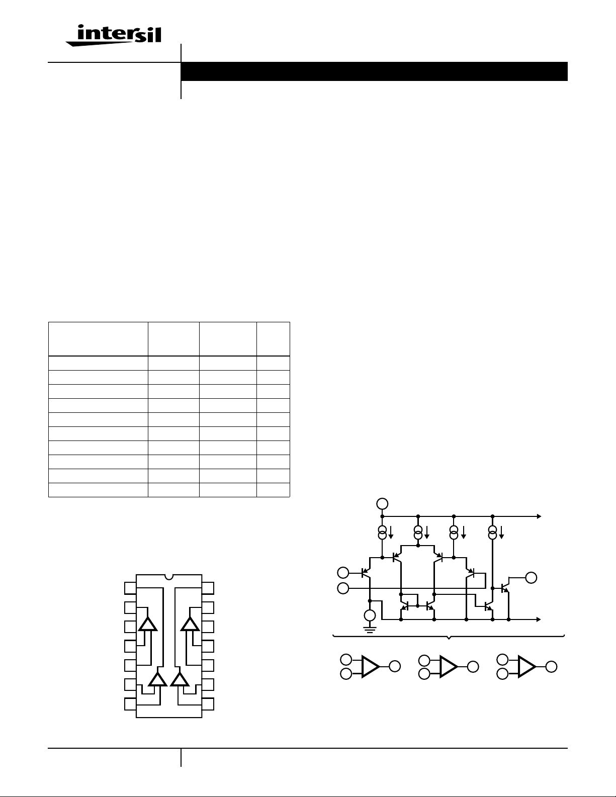
Ordering Information
TEMP.
RANGE
PART NO. (BRAND)
CA0139E -55 to 125 14 Ld PDIP E14.3
CA0139M, AM (139, 139A) -55 to 125 14 Ld SOIC M14.15
CA0239E -25 to 85 14 Ld PDIP E14.3
CA0239M96 (239) -25 to 85 14 Ld SOIC M14.15
CA0339E 0 to 70 14 Ld PDIP E14.3
CA0339M (339) 0 to 70 14 Ld SOIC M14.15
LM339N 0 to 70 14 Ld PDIP E14.3
LM2901N -40 to 85 14 Ld PDIP E14.3
LM3302M96 (3302) -40 to 85 14 Ld SOIC M14.15
LM3302N -40 to 85 14 Ld PDIP E14.3
(oC) PACKAGE
PKG.
NO.
Pinout
CA139A (SOIC)
CA139, CA339, LM3302 (PDIP, SOIC)
CA239, LM2901, LM339 (PDIP)
TOP VIEW
OUTPUT 2
OUTPUT 1
V+
1
2
1 4
3
14
13
12
OUTPUT 3
OUTPUT 4
GND
File Number 795.6
Features
• Operation from Single or Dual Supplies
• Common Mode Input Voltage Range to GND
• Output Voltage Compatible with TTL, DTL, ECL,
MOS and CMOS
• Differential Input Voltage Range Equal to the
Supply Voltage
• Maximum Input Offset Voltage (VIO)
- CA139A . . . . . . . . . . . . . . . . . . . . . . . . . . . . . . . . . 2mV
- CA139, CA239, CA339. . . . . . . . . . . . . . . . . . . . . . 5mV
- LM2901. . . . . . . . . . . . . . . . . . . . . . . . . . . . . . . . . . 7mV
- LM3302. . . . . . . . . . . . . . . . . . . . . . . . . . . . . . . . . 20mV
• Replacement for Industry Types 139, 239, 339, 139A,
2901, 3302
Applications
• Square Wave Generator
• Time Delay Generators
• Pulse Generators
• Multivibrators
• High Voltage Digital Logic Gates
• A/D Converters
• MOS Clock Timers
Schematic Diagram
V+
+ INPUT
5
4
- INPUT
3
3.5µA
Q
1
Q
5
12
100µA 3.5µA 100µA
Q
Q
3
2
Q
4
Q
6
TO 2, 3, 4
OUTPUT
2
Q
8
Q
7
TO 2, 3, 4
NEG. INPUT 1
POS. INPUT 1
NEG. INPUT 2
POS. INPUT 2
4
5
2 3
6
7
1
POS. INPUT 4
11
NEG. INPUT 4
10
POS. INPUT 3
9
NEG. INPUT 3
8
COMPARATOR NO 1
+
7
-
6
CAUTION: These devices are sensitive to electrostatic discharge; follow proper IC Handling Procedures.
1-888-INTERSIL or 321-724-7143
1
2
+
11
4
-
10
13
| Copyright © Intersil Corporation 1999
+
9
-
8
3
14
CA139, CA139A, CA239, CA339, LM339, LM2901, LM3302
Absolute Maximum Ratings Thermal Information
Supply Voltage. . . . . . . . . . . . . . . . . . . . . . . . . . . . . . . .36V or ±18V
Differential Input Voltage . . . . . . . . . . . . . . . . . . . . . . . . . . . . . . .36V
Input Voltage . . . . . . . . . . . . . . . . . . . . . . . . . . . . . . . .-0.3V to +36V
Input Current (VI < -0.3V, Note 1) . . . . . . . . . . . . . . . . . . . . . . 50mA
Output Short Circuit Duration (Single Supply, Note 2). . .Continuous
Operating Conditions
Temperature Range
CA139, CA139A. . . . . . . . . . . . . . . . . . . . . . . . . . -55oC to 125oC
CA239 . . . . . . . . . . . . . . . . . . . . . . . . . . . . . . . . . . -25oC to 80oC
CA339, LM339 . . . . . . . . . . . . . . . . . . . . . . . . . . . . . 0oC to 70oC
LM2901, LM3302 . . . . . . . . . . . . . . . . . . . . . . . . . . -40oC to 85oC
CAUTION: Stresses above those listed in “Absolute Maximum Ratings” may cause permanent damage to the device. This is a stress only rating and operation of the
device at these or any other conditions above those indicated in the operational sections of this specification is not implied.
NOTES:
1. Inputs must not go more negative than -0.3V.
2. Shortcircuitsfrom the output to V+ can cause excessive heating and eventual destruction. The maximum output current independent of V+is
approximately 20mA.
3. θJA is measured with the component mounted on an evaluation PC board in free air.
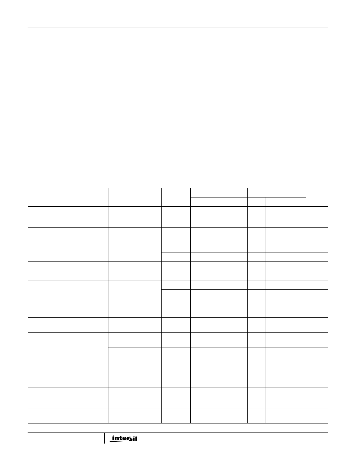
Electrical Specifications V+ = 5V, Unless Otherwise Specified
TEST
PARAMETER SYMBOL
Input Offset Voltage V
Differential Input Voltage V
IO
ID
CONDITIONS
V
= 1.4V, RS = 0,
REF
Output Switch Point
V ≅ 1.4V
Keep All Inputs ≥0V , or
V- (if used), (Note 5)
Saturation Voltage V
Common Mode Input
Voltage Range
Input Offset Current I
Input Bias Current I
Total Supply Current I+ RL = ∞ On All
Output Leakage
Current
Output Sink Current VI- ≥ 1V, VI+ = 0V,
Voltage Gain A
Large Signal Response
Time
Response Time
(Figures 3, 4)
V
VI- = 1V, VI+ = 0V,
SAT
I
≤ 4mA
SINK
Note 6 TA = 25 0 - V+ -1.5 0 - V+ -1.5 V
ICR
II+ - II-T
IO
II+ or II- with Output in
IB
Linear Range
Comparators
VI+ ≥ 1V, VI- = 0V,
VO = 5V
VI+ ≥ 1V, VI- = 0V,
VO = 30V
VO≤ 1.5V
RL≥ 15kΩ, V+ = 15V TA = 25 - 200 - 50 200 - V/mV
OL
VI = TTL Logic Swing,
V
= 1.4V, VRL = 5V,
REF
RL = 5.1kΩ
VRL = 5V, RL = 5.1kΩ TA = 25 - 1.3 - - 1.3 - µs
TEMP
TA = 25 - 2 5 - 1 2 mV
Note 4 - - 9 - - 4 mV
Note 4 - - 36 - - 36 V
TA = 25 - 250 400 - 250 400 mV
Note 4 - - 700 - - 700 mV
Note 4 0 - V+ -2 0 - V+ -2 V
A
Note 4 - - 100 - - 100 nA
TA = 25 - 25 100 - 25 100 nA
Note 4 - - 300 - - 300 nA
TA = 25 - 0.8 2 - 0.8 2 mA
TA = 25 - 0.1 - - 0.1 - nA
Note 4 - - 1 - - 1 µA
TA = 25 6 16 - 6 16 - mA
TA = 25 - 300 - - 300 - ns
Thermal Resistance (Typical, Note 3) θJA (oC/W) θJC (oC/W)
PDIP Package . . . . . . . . . . . . . . . . . . . 100 N/A
SOIC Package . . . . . . . . . . . . . . . . . . . 175 N/A
Maximum Junction Temperature (Plastic Package). . . . . . . . .150oC
Maximum Storage Temperature Range. . . . . . . . . . -65oC to 150oC
Maximum Lead Temperature (Soldering 10s) . . . . . . . . . . . . 300oC
(SOIC - Lead Tips Only)
CA139 CA139A
(oC)
= 25 - 3 25 - 3 25 nA
UNITSMIN TYP MAX MIN TYP MAX
2

CA139, CA139A, CA239, CA339, LM339, LM2901, LM3302
Electrical Specifications V+ = 5V, Unless Otherwise Specified
CA239, CA339, LM339
UNITSMIN TYP MAX
PARAMETER SYMBOL
Input Offset Voltage V
TEST
CONDITIONS
V
IO
= 1.4V, RS = 0, Output Switch
REF
TEMP
o
(
C)
TA = 25 - 2 5 mV
Point V ≅ 1.4V
Note 4 - - 9 mV
Differential Input Voltage V
ID
Keep All Inputs ≥ 0V, or V- (if used)
Note 4 - - 36 V
(Note 5)
Saturation Voltage V
SAT
VI- = 1V, VI+ = 0V, I
≤ 4mA TA = 25 - 250 400 mV
SINK
Note 4 - - 700 mV
Common Mode Input
V
ICR
Note 6 TA = 25 0 - V+ -1.5 V
Voltage Range
Note 4 0 - V+ - 2 V
Input Offset Current I
IO
II+ - II-T
= 25 - 5 50 nA
A
Note 4 - - 150 nA
Input Bias Current I
IB
II+ or II- with Output in Linear Range TA = 25 - 25 250 nA
Note 4 - - 400 nA
Total Supply Current I+ RL = ∞ on All Comparators TA = 25 - 0.8 2 mA
Output Leakage Current VI+ ≥ 1V, VI- = 0V, VO = 5V TA = 25 - 0.1 - nA
VI+ ≥ 1V, VI- = 0V, VO = 30V Note 4 - - 1 µA
Output Sink Current VI- ≥ 1V, VI+ = 0V, VO≤ 1.5V TA = 25 6 16 - mA
Voltage Gain A
Large SignalResponse Time
Response Time
OL
RL≥ 15kΩ, V+ = 15V TA = 25 50 200 - V/mV
VI= TTL Logic Swing, V
V
=5V, RL = 5.1kΩ
RL
REF
= 1.4V,
TA = 25 - 300 - ns
VRL = 5V, RL = 5.1kΩ TA = 25 - 1.3 - µs
(Figures 3, 4)
NOTES:
4. Ambient Temperature (TA) applicable over operating temperature range as shown below.
CA139, CA139A = -55oC to 125oC; CA239 = -25oC to 85oC; CA339, LM339 = 0oC to 70oC; LM2901, LM3302 = -40oC to 85oC.
5. Thecomparatorwillprovide a proper output state even if the positive swing of the inputs exceeds the power supply voltage level, if the other
input remains withinthe common mode voltage range.Thelow input voltage state mustnot be less than -0.3V(or0.3V below the magnitude of
the negative power supply, if used).
6. The upper end of the common mode voltage range is (V+) - 1.5V, but either or both inputs can go to +30V without damage.
3

CA139, CA139A, CA239, CA339, LM339, LM2901, LM3302
Electrical Specifications V+ = 5V, Unless Otherwise Specified
TEST
PARAMETER SYMBOL
Input Offset Voltage V
IO
CONDITIONS
V
= 1.4V, RS = 0,
REF
Output Switch Point
V ≅ 1.4V
Differential Input Voltage V
Keep All Inputs≥ 0V , or
ID
V- (if used), (Note 5)
Saturation Voltage V
Common Mode Input
V
SAT
ICR
VI- = 1V, VI+ = 0V,
I
≤ 4mA
SINK
Note 6 TA = 25 0 - V+ - 1.5 0 - V+ -1.5 V
Voltage Range
Input Offset Current I
Input Bias Current I
II+ - II-T
IO
II+orII- withOutputin
IB
Linear Range
Total Supply Current I+ RL = ∞ on All
Comparators
Output Leakage Current VI+ ≥ 1V, VI- = 0V,
VO = 5V
VI+ ≥ 1V, VI- = 0V,
VO = 30V
Output Sink Current VI- ≥ 1V, VI+ = 0V,
VO≤ 1.5V
Voltage Gain A
Large Signal Response
Time
RL≥ 15kΩ, V+ = 15V TA = 25 25 100 - 2 30 - V/mV
OL
VI = TTL Logic Swing,
V
= 1.4V,
REF
VRL=5V, RL = 5.1kΩ
Response Time
VRL = 5V, RL = 5.1kΩ TA = 25 - 1.3 - - 1.3 - µs
(Figures 3, 4)
TEMP
(
TA = 25 - 2 7 - 1 20 mV
Note 4 - - 15 - - 40 mV
Note 4 - - 36 - - 28 V
TA = 25 - 250 400 - 250 500 mV
Note 4 - - 700 - - 700 mV
Note 4 0 - V+ - 2 0 - V+ -2 V
A
Note 4 - - 200 - - 300 nA
TA = 25 - 25 250 - 25 500 nA
Note 4 - - 500 - - 1000 nA
TA = 25 - 0.8 2 - 0.8 2 mA
TA = 25 - 0.1 - - 0.1 - nA
Note 4 - - 1 - - 1 µA
TA = 25 6 16 - 6 16 - mA
TA = 25 - 300 - - 300 - ns
LM2901 LM3302
o
C)
UNITSMIN TYP MAX MIN TYP MAX
= 25 - 5 50 - 3 100 nA
Typical Performance Curves
RL = ∞
1.0
0.8
0.6
0.4
SUPPLY CURRENT (mA)
0.2
0102030
POSITIVE SUPPLY VOLTAGE (V)
-55oC
0oC
25oC
70oC
125oC
INPUT CURRENT (nA)
FIGURE 1. SUPPLY CURRENT vs SUPPLY VOLTAGE FIGURE 2. INPUT CURRENT vs SUPPLY VOLTAGE
4
VIC = 0V
R
= 109Ω
IC
60
50
40
30
20
10
010203040
POSITIVE SUPPLY VOLTAGE (V)
-55oC
0oC
o
25
o
70
125
C
C
o
C

CA139, CA139A, CA239, CA339, LM339, LM2901, LM3302
Typical Performance Curves
TA = 25oC
V+ = +5V
3
V
I
4
-
+
5
5
4
3
2
1
0
OUTPUT VOLTAGE (V)
100mV
20mV
0 0.5 1.0 1.5 2.0
TIME (µs)
12
INPUT
OVERDRIVE
= 5mV
5.1kΩ
2
V
0
-50
-100
INPUT VOLTAGE (mV)
O
5
4
3
2
1
OUTPUT VOLTAGE (V)
0
V+ = +5V
3
V
I
4
-
+
5
12
0 0.5 1.0 1.5 2.0
5.1kΩ
2
100mV
TIME (µs)
V
O
20mV
TA = 25oC
INPUT
OVERDRIVE
= 5mV
100
50
0
INPUT VOLTAGE (mV)
FIGURE 3. RESPONSE TIME FOR VARIOUS INPUT
OVERDRIVES - NEGATIVE TRANSITION
1
10
0
10
-1
10
-2
10
OUTPUT SATURATION VOLTAGE (V)
-3
10
10
FIGURE 5. OUTPUT SATURATION VOLTAGE vs OUTPUT SINK CURRENT
Metallization Mask Layout
0
10 20 30 40 50 55
54
50
TA = 25oC
-2
FIGURE 4. RESPONSE TIME FOR VARIOUS INPUT
OUT OF
SATURATION
-1
10
OUTPUT SINK CURRENT (mA)
0
10
OVERDRIVES - POSITIVE TRANSITION
1
10
2
10
40
NOTE: Dimensions in parentheses
30
20
10
0
4 - 10 (0.102 - 0.254)
52 - 60 (1.321 - 1.524)
51 -5 9
(1.295 - 1.499)
are in mm and are derived from the
basic in. dimensions as indicated. Grid
graduations are in mils (10-3 inch).
5

CA139, CA139A, CA239, CA339, LM339, LM2901, LM3302
All Intersil semiconductor products are manufactured, assembled and tested under ISO9000 quality systems certification.
Intersil semiconductor products are sold by description only. Intersil Corporation reserves the right to make changes incircuit design and/or specifications at any time without notice. Accordingly, the reader is cautioned to verify that data sheets are current before placing orders. Information furnished by Intersil is believed to be accurate and
reliable. However, no responsibility is assumed by Intersil or its subsidiaries forits use; nor for any infringements of patents or other rights of third parties which may result
from its use. No license is granted by implication or otherwise under any patent or patent rights of Intersil or its subsidiaries.
For information regarding Intersil Corporation and its products, see web site www.intersil.com
Sales Office Headquarters
NORTH AMERICA
Intersil Corporation
P. O. Box 883, Mail Stop 53-204
Melbourne, FL 32902
TEL: (321) 724-7000
FAX: (321) 724-7240
6
EUROPE
Intersil SA
Mercure Center
100, Rue de la Fusee
1130 Brussels, Belgium
TEL: (32) 2.724.2111
FAX: (32) 2.724.22.05
ASIA
Intersil (Taiwan) Ltd.
7F-6, No. 101 Fu Hsing North Road
Taipei, Taiwan
Republic of China
TEL: (886) 2 2716 9310
FAX: (886) 2 2715 3029
 Loading...