


现货库存、技术资料、百科信息、热点资讯,精彩尽在鼎好!
R
P
E
T
E
L
O
S
B
O
C
E
R
O
N
E
M
M
O
R
D
E
D
N
T
C
U
D
O
A
L
P
E
N
E
M
E
C
Data Sheet May 2001
CA124, CA224, CA324, LM324, LM2902
T
File Number 796.5
Quad, 1MHz, Operational Amplifiers for
Commercial, Industrial, and Military
Applications
itle
The CA124,CA224, CA324, LM324, and LM2902 consist of
12
four independent, high-gainoperational amplifiers on a
single monolithic substrate. An on-chip capacitor in each of
224
the amplifiers provides frequency compensationfor unity
gain. These devices are designed specially to operatefrom
324
either single or dual supplies, and the differential voltage
range is equal tothe power-supplyvoltage. Low power drain
and an inputcommon-mode voltage range from 0V to V+
324
-1.5V (single-supply operation) make these devices suitable
for battery operation.
290
Part Number Information
b-
ad,
Hz,
ra-
al
pli-
s
-
-
,
usl,
i-
li-
s)
tho
PART
NUMBER
(BRAND)
CA0124E -55 to 125 14 Ld PDIP E14.3
CA0124M
(124)
CA0124M96
(124)
CA0224E -40 to 85 14 Ld PDIP E14.3
CA0224M
(224)
CA0324E 0 to 70 14 Ld PDIP E14.3
CA0324M
(324)
CA0324M96
(324)
LM324N 0 to70 14 Ld PDIP E14.3
LM2902N -40 to85 14 Ld PDIP E14.3
LM2902M
(2902)
LM2902M96
(2902)
TEMP.
RANGE (
o
C) PACKAGE
-55 to 125 14 Ld SOIC M14.15
-55 to 125 14 Ld SOIC Tape and
-40to85 14LdSOIC M14.15
0to70 14LdSOIC M14.15
0to70 14LdSOICTapeand
-40to85 14LdSOIC M14.15
-40to85 14LdSOICTapeand
Reel
Reel
Reel
PKG.
NO.
M14.15
M14.15
M14.15
Features
• Operation f rom Single or Dual Supplies
• Unity-GainBandwidth ...................1MHz(Typ)
• DCVoltageGain ......................100dB(Typ)
• InputBiasCurrent ......................45nA(Typ)
• InputOffsetVoltage.....................2mV(Typ)
• Input Offset Current
- CA224, CA324,LM324, LM2902 . . ........5nA(Typ)
- CA124...............................3nA(Typ)
• Replacement for Industry Types 124, 224, 324
Applications
• Summing Amplifiers
• Multivibrators
• Oscillators
• Transducer Amplifiers
• DC Gain Blocks
Pinout
CA124, CA224, CA324, LM2902 (PDIP, SOIC)
OUTPUT 1
NEG.
INPUT 1
POS.
INPUT 1
V+
POS.
INPUT 2
NEG.
INPUT 2
OUTPUT 2
LM324 (PDIP)
1
2
3
4
5
6
7
TOP VIEW
1
+
+2+
14
OUTPUT 4
13
12
11
10
9
8
NEG.
INPUT 4
POS.
INPUT 4
VPOS.
INPUT 3
NEG.
INPUT 3
OUTPUT 3
4
+
3
y-
ds
er-
1
1-888-INTERSIL or 321-724-7143
CAUTION: These devices aresensitiveto electrostatic discharge;followproperIC Handling Procedures.
| Intersil and Design is a trademarkof IntersilAmericasInc. | Copyright © Intersil Americas Inc. 2001
CA124, CA224, CA324, LM324, LM2902
Absolute Maximum Ratings Thermal Information
SupplyVoltage................................32Vor±16V
DifferentialInputVoltage...............................32V
InputVoltage.................................-0.3Vto32V
Input Current (V
OutputShort Circuit Duration(V+ ≤ 15V, Note 2) . . . . . .Continuous
<-0.3V,Note1) ......................50mA
I
Operating Co nditions
TemperatureRange
CA124 .................................-55
CA224,LM2902...........................-40
CA324,LM324..............................0
CAUTION: Stresses above those listed in “Absolute Maximum Ratings” may cause permanent damage to the device. This is a stress only rating and operationofthe
device at these or any other conditions above those indicated in the operational sections of this specification is not implied.
NOTES:
1. This inputcurrent will onlyexist when the voltage at any of theinput leads is driven negative. This currentis due to the collectorbase junction of the
input p-n-p transistorsbecoming forward biased and thereby actingas input diode clamps.In additionto this diode action, thereis also lateral n-p-n
parasitictransistor action on the ICchip.Thistransistoractioncan cause the output voltagesof the amplifiers to go totheV+voltagelevel (or to ground
for a large overdrive) for the time duration that an input is driven negative. Thistransistoraction isnot destructive and normal outputstates will reestablishwhen theinput voltage, whichwas negative, again returns to a valuegreater than -0.3V.
2. The maximum output current is approximately 40mA independentof the magnitudeof V+. Continuousshortcircuits at V+ > 15V can cause
excessive power dissipationand eventual destruction. S hort circuits from theoutput to V+ can cause overheating andeventual destruction of
the device.
3. θ
is measured with thecomponent mountedon an evaluation PC board in freeair.
JA
o
Cto125oC
o
Cto85oC
o
Cto70oC
Thermal Resistance (Typical, Note 3) θ
JA
(oC/W)
PDIPPackage............................. 95
SOICPackage............................. 175
MaximumJunctionTemperature(Die)...................175
MaximumJunctionTemperature (Plastic Package). . . . . . . . .150
MaximumStorageTemperatureRange..........-65
o
Cto150oC
MaximumLead Temperature(Soldering 10s) . . . . . . . . . .. . .300
(SOIC - LeadTips Only)
o
C
o
C
o
C
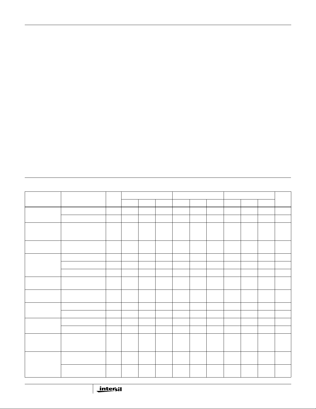
Electrical Specifications ValuesApply for EachOperational Amplifier.Supply Voltage V+ = 5V, V- = 0V,
UnlessOtherwise Specified
CA124 CA224, CA324, LM324 LM2902
PARAMETER
Input Offset
Voltage (Note 6)
Average Input
Offset Voltage
Drift
DifferentialInput
Voltage (Note 5)
Input Common
Mode Voltage
Range (Note 5)
Common Mode
Rejection Ratio
Power Supply
Rejection Ratio
InputBias
Current (Note 4)
Input Offset
Current
Average Input
Offset Current
Drift
Large Signal
Voltage Gain
TEST
CONDITIONS
TEMP.
o
C)
(
25-25-27---mV
Full--7--9--10mV
=0Ω Full-7--7--7-µV/oC
R
S
Full--V+--V+--V+V
V+ = 30V 25 0 - V+ -1.5 0 - V+ -1.5 - - - V
V+ = 30V Full 0 - V+ -2 0 - V+ -2 - - - V
V+=26V Full------0-V+-2V
DC 25 70 85 - 65 70 - - - - dB
DC 25 65 100 - 65 100 - - - - dB
I
+orII- 25 - 45 150 - 45 250 - - - nA
I
+orII- Full - - 300 - - 500 - 40 500 nA
I
I
+-II- 25- 330- 550- - -nA
I
I
+-II- Full - - 100 - - 150 - 45 200 nA
I
I
Full-10- -10- -10-pA/
R
≥ 2kΩ,V+=15V
L
(For Large V
≥ 2kΩ,V+=15V
R
L
(ForLarge V
Swing)
O
O
Swing)
25 94 100 - 88 100 - - - - dB
Full 88 - - 83 - - 83 - - dB
UNITSMIN TYP MAX MIN TYP MAX MIN TYP MAX
o
C
2

CA124, CA224, CA324, LM324, LM2902
Electrical Specifications ValuesApply for EachOperational Amplifier.Supply Voltage V+ = 5V, V- = 0V,
UnlessOtherwise Specified (Continued)
CA124 CA224, CA324, LM324 LM2902
UNITSMIN TYP MAX MIN TYP MAX MIN TYP MAX
PARAMETER
Output
Voltage
Swing
Output
Current
High
Level
Low
Level
Source V
TEST
CONDITIONS
R
=2kΩ 250-V+-1.50-V+-1.5---V
L
= 2kΩ, V+ = 30V Full 26 - - 26 - - - - - V
R
L
= 2kΩ,V+=26VFull------22--V
R
L
=10kΩ, V+ = 30V Full 27 28 - 27 28 - 23 28 - V
R
L
=10kΩ Full-520-520-5100mV
R
L
+=+1V,VI-=0V,
I
V+ = 15V
V
+=1V,VI-=0,
I
TEMP.
o
C)
(
25 20 40 - 2 0 40 - - - - mA
Full 10 20 - 10 20 - 10 20 - mA
V+ = 15V
Sink V
Crosstalk f = 1 to 20kHz
+=0V,VI-=1V,
I
V+ = 15V
+=0V,VI-=1V,
V
I
V
=200mV
O
-=1V,VI+=0,
V
I
V+ = 15V
25 10 20 - 1 0 20 - - - - mA
25 12 50 - 12 50 - - - - µA
Full58-58-58 -mA
25 - -120 - - -120 - - - - dB
(InputReferred)
Total Supply
Current
R
= ∞ Full-0.82 -0.82 -0.71.2mA
L
= ∞,V+=26VFull-------1.53mA
R
L
NOTES:
4. Due to t he PNP inputstage the directionof the input currentis out ofthe IC. No loading change existson theinput lines because the currentis
essentially constant, independentof the state ofthe output.
5. The input signal voltageand the input common mode voltageshouldnot be allowed to go negativeby more than0.3V. T he positivelimit of the
commonmode voltage range is V+ - 1.5V, but either or both inputs can go to +32V without damage.
=1.4V,RS=0Ω with V+ from5V to 30V, and over the full input common modevoltagerange (0V toV+ - 1.5V).
6. V
O
Schematic Diagram (One of FourOperational Amplifiers)
V+
4
INPUTS
6µA
Q
Q
2
-
+
Q
1
3
Q
8
3
2
Q
9
11
V-
3
4µA
C
COMP
Q
4
Q
11
Q
10
TO 2, 3, 4
100
µA
5
+
2 7
-
Q
5
Q
6
Q
7
R
SC
V
1
Q
13
Q
12
50µA
TO 2, 3, 4
6
12
+
4 4
-
13
10
O
+
3 8
-
9

CA124, CA224, CA324, LM324, LM2902
Typical Performance Curves
140
TA=-40≤ TA≤ 85oC
120
100
80
60
40
V+=10TO15V
20
OPEN-LOOP VOLTAGE GAIN (dB)
0
1 10 100 1K 10K 100K 1M 10M
0.1µF
2
V
I
V+/2
FREQUENCY (Hz)
4
-
+
3
11
V+=26V
V+
1
V
O
TA=25oC
V+ = 30V
500
2
-
450
400
350
300
OUTPUT VOLTAGE (mV)
250
0123456789
OUTPUT
+
3
50pF
V
I
1
TIME (µs)
V
O
FIGURE 1. OPEN LOOP FREQUENCY RESPONSE FIGURE 2. VOLTAGEFOLLOWER PULSE RESPONSE
(SMALL SIGNAL)
TA=25oC
V+ = 15V
R
=2kΩ
L
4
3
2
1
0
4
3
2
1
INPUT VOLTAGE (V)
010203040
TIME (µs)
OUTPUT VOLTAGE (V)
INPUT
FIGURE 3. VOLTAGE FOLLOWER PULSE RESPONSE (LARGE SIGNAL)
V
=0V
ICR
60
50
40
30
20
INPUT CURRENT (nA)
10
0
-75 -50 -25 0 25 50 75 100 125
V+=30V
15V
5V
TEMPERATURE (oC)
4
3
2
SUPPLYCURRENT (mA)
1
0
TA=0oC TO 125oC
-55oC
0 5 10 15 20 25 30
POSITIVE SUPPLY VOLTAGE (V)
2
3
-
+
mA
11
V+
I
D
4
FIGURE 4. INPUT CURRENT vs AMBIENT TEMPERATURE FIGURE 5. SUPPLY CURRENT vs SUPPLY VOLTAGE
4
1

CA124, CA224, CA324, LM324, LM2902
Typical Performance Curves (Continued)
20
TA=25oC
15
10
5
OUTPUT VOLTAGE SWING (V)
0
1K 10K 100K 1M
FREQUENCY (Hz)
1kΩ
+7V
V
I
100kΩ
+15V
4
2
-
+
3
11
V
O
1
2kΩ
70
V+ = 15V
60
50
40
30
20
10
OUTPUT SOURCE CURRENT (mA)
0
-75 -50 -25 0 25 50 75 100 125
TEMPERATURE(oC)
FIGURE 6. LARGE SIGNAL FREQUENCY RESPONSE FIGURE 7. OUTPUT CURRENT vs AMBIENT TEMPERATURE
TA=25oC
75
50
150
125
100
TA=25oC
RL=20kΩ
RL=2kΩ
75
25
INPUT CURRENT (nA)
0 10203040
POSITIVE SUPPLYVOLTAGE (V)
50
25
OPEN LOOP VOLTAGE GAIN (dB)
0
0 10203040
POSITIVE SUPPLY VOLTAGE (V)
FIGURE 8. INPUT CURRENT vs SUPPLYVOLTAGE FIGURE 9. VOLTAGE GAIN vs SUPPLY VOLTAGE
5

CA124, CA224, CA324, LM324, LM2902
Dual-In-Line Plastic Packages (PDIP)
N
D1
-C-
E1
-B-
A1
A2
E
A
L
e
C
C
L
e
A
C
e
B
INDEX
AREA
BASE
PLANE
SEATING
PLANE
D1
B1
12 3 N/2
-AD
e
B
0.010 (0.25) C AM BS
NOTES:
1. Controlling Dimensions: INCH. In case of conflict between English
and Metric dimensions, the inch dimensions control.
2. Dimensioningand tolerancingper ANSI Y14.5M-1982.
3. Symbols are defined in the “MO Series Symbol List” in Section 2.2 of
Publication No. 95.
4. Dimensions A, A1and L aremeasured with the package seated in
JEDECseating plane gauge GS-3.
5. D, D1, and E1 dimensions do notinclude mold flash or protrusions.
Mold flash or protrusions shall notexceed 0.010inch (0.25mm).
6. E and are measured with the leads constrainedt o be perpen-
7. e
e
dicular to datum .
A
and eCare measured at the lead tips withthe leads uncon-
B
strained. e
-C-
must be zero or greater.
C
8. B1maximumdimensionsdonotinclude dambarprotrusions. Dambar
protrusions shall not exceed 0.010 inch (0.25mm).
9. N is the maximum number of terminal positions.
10. Cornerleads(1,N, N/2 andN/2 + 1)for E8.3, E16.3,E18.3,E28.3,
E42.6 will have a B1 dimension of 0.030 - 0.045 inch (0.76 -
1.14mm).
E14.3 (JEDEC MS-001-AA ISSUE D)
14 LEAD DUAL-IN-LINE PLASTIC PACKAGE
INCHES MILLIMETERS
SYMBOL
A - 0.210 - 5.33 4
A1 0.015 - 0.39 - 4
A2 0.115 0.195 2.93 4.95 -
B 0.014 0.022 0.356 0.558 B1 0.045 0.070 1.15 1.77 8
C 0.008 0.014 0.204 0.355 -
D 0.735 0.775 18.66 19.68 5
D1 0.005 - 0.13 - 5
E 0.300 0.325 7.62 8.25 6
E1 0.240 0.280 6.10 7.11 5
e 0.100 BSC 2.54 BSC -
e
A
e
B
0.300 BSC 7.62 BSC 6
- 0.430 - 10.92 7
L 0.115 0.150 2.93 3.81 4
N14 149
NOTESMINMAXMINMAX
Rev. 0 12/93
6

CA124, CA224, CA324, LM324, LM2902
Small Outline Plastic Packages (SOIC)
N
INDEX
AREA
123
SEATING PLANE
-AD
e
B
0.25(0.010) C AM BS
M
E
-B-
A
-C-
0.25(0.010) BM M
H
α
µ
A1
0.10(0.004)
L
hx45
o
C
NOTES:
1. Symbolsaredefinedin the “MO Series Symbol List” in Section 2.2 of
Publication Number 95.
2. Dimensioningand tolerancingper ANSI Y14.5M-1982.
3. Dimension “D” does not include mold flash, protrusions or gate burrs.
Moldflash,protrusionand gate burrsshallnotexceed0.15mm (0.006
inch) per side.
4. Dimension“E”doesnotincludeinterleadflashorprotrusions. Interlead
flashand protrusionsshall not exceed 0.25mm (0.010 inch) perside.
5. The chamfer on the body is optional. If it is not present, a visual index
feature must be located within the crosshatched area.
6. “L” is the length of terminal for soldering to a substrate.
7. “N” is the number of terminal positions.
8. Terminalnumbers areshown for referenceonly.
9. The lead width “B”, as measured 0.36mm (0.014 inch) or greater
above the seating plane, shall not exceed a maximum value of
0.61mm (0.024 inch).
10. Controllingdimension: MILLIMETER.Convertedinch dimensions
are not necessarily exact.
M14.15 (JEDEC MS-012-AB ISSUE C)
14 LEAD NARROW BODY SMALL OUT LINE PLASTIC
PACKAGE
INCHES MILLIMETERS
SYMBOL
A 0.0532 0.0688 1.35 1.75 -
A1 0.0040 0.0098 0.10 0.25 -
B 0.013 0.020 0.33 0.51 9
C 0.0075 0.0098 0.19 0.25 D 0.3367 0.3444 8.55 8.75 3
E 0.1497 0.1574 3.80 4.00 4
e 0.050 BSC 1.27 BSC -
H 0.2284 0.2440 5.80 6.20 -
h 0.0099 0.0196 0.25 0.50 5
L 0.016 0.050 0.40 1.27 6
N14 147
o
α
0
o
8
o
0
o
8
Rev. 0 12/93
NOTESMINMAXMINMAX
-
All Intersilproducts are manufactured, assembled and tested utilizing ISO9000 quality systems.
Intersil Corporation’s qualitycertifications canbe viewed at website www.intersil.com/design/quality/iso.asp
Intersil products are sold by description only. Intersil Corporation reserves the right to make changes in circuit design and/or specifications at any time without notice.
Accordingly, the reader is cautioned to verify that datasheets are currentbefore placi ngorders. Information furnished by Intersil is believed tobe accurateand reliable.However,no responsi bility is assumed by Intersilor itssubsidiaries for its use;nor forany infringements of patents or other rights of third parties which may result from its use. No
license is granted by implication or otherwise under any patent or patentrights of Intersil or its subsidiaries.
.
For information regarding Intersil Corporation and its products, see web site www.intersil.com
Sales Office Headquarters
NORTH AMERICA
Intersil Corporation
2401 Palm Bay Rd.
Palm Bay, FL 32905
TEL: (321) 724-7000
FAX: (321) 724-7240
EUROPE
Intersil SA
MercureCenter
100,RuedelaFusee
1130 Brussels, Belgium
TEL: (32) 2.724.2111
FAX: (32) 2.724.22.05
7
ASIA
Intersil Ltd.
8F-2,96, Sec. 1,Chien-kuo North,
Taipei, Taiwan 104
Republic of China
TEL: 886-2-2515-8508
FAX: 886-2-2515-8369
 Loading...