

现货库存、技术资料、百科信息、热点资讯,精彩尽在鼎好!
CA158, CA158A, CA258, CA358, CA358A,
CA2904, LM358, LM2904
Data Sheet October 1999
Dual, 1MHz, Operational Amplifiers for
Commercial Industrial, and Military
Applications
The CA158, CA158A, CA258, CA358, CA358A and CA2904
types consist of two independent, high gain, internally
frequency compensated operational amplifiers which are
designed specifically to operate from a single power supply
over a wide range of voltages. They may also be operated
from split power supplies. The supply current is basically
independent of the supply voltage over the recommended
voltage range.
These devicesareparticularly usefulininterface circuitswith
digital systems and can be operated from the single
common 5VDC power supply. They are also intended for
transducer amplifiers, DC gain blocks and many other
conventional op amp circuits which can benefit from the
single power supply capability.
The CA158, CA158A, CA258, CA358, CA358A, and
CA2904 types are an equivalent to or a replacement for the
industry types 158, 158A, 258, 258A, 358, 358A, and
CA2904.
Technical Data on LM Branded types is identical to the
corresponding CA Branded types.
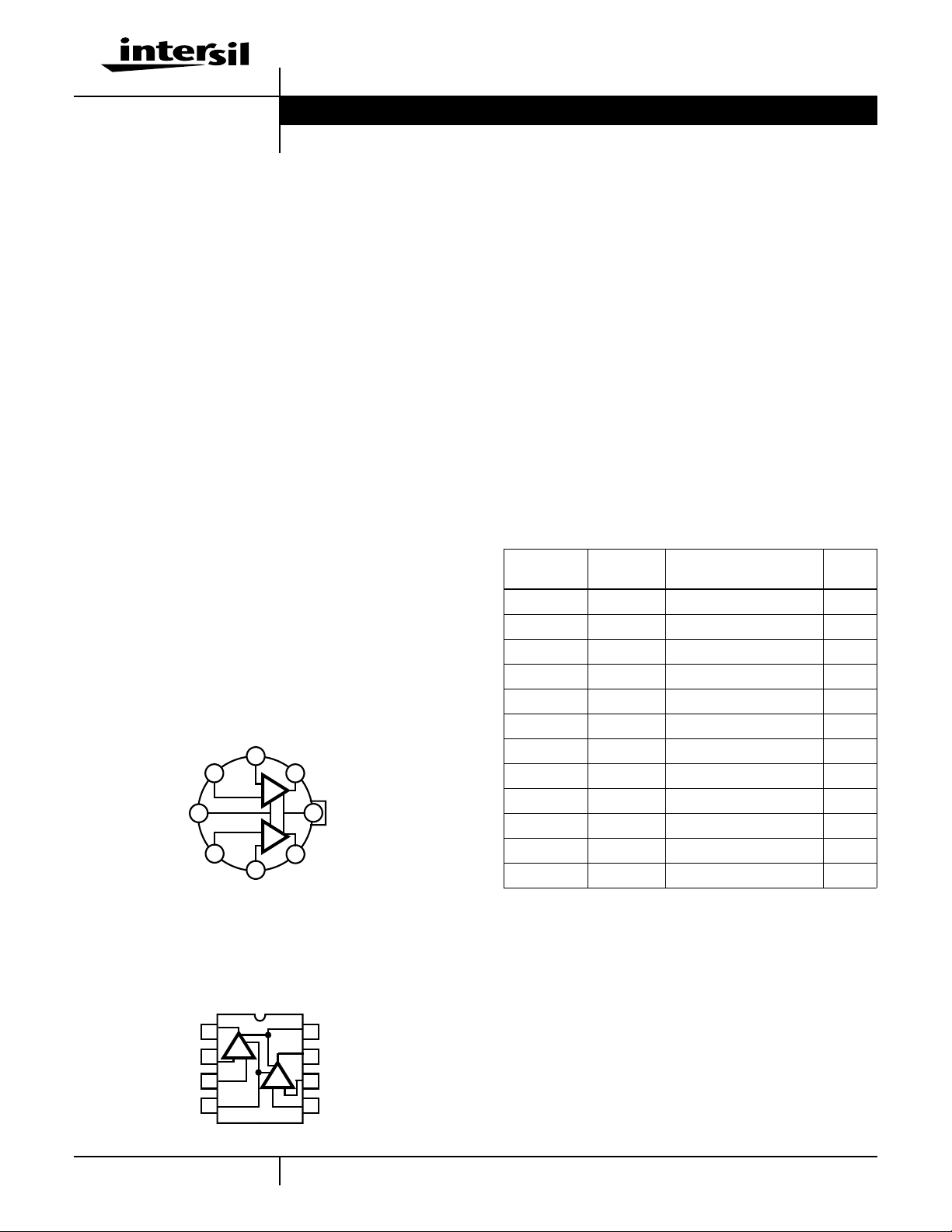
Pinouts
CA158 (METAL CAN)
TOP VIEW
INV.
INPUT (A)
NON-INV.
INPUT (A)
V-
NON-INV.
INPUT (B)
4
3
5
2
-
A
+
+
B
-
6
INV.
INPUT (B)
OUTPUT (A)
1
8
7
OUTPUT (B)
V+
File Number 1019.6
Features
• Internal Frequency Compensation for Unity Gain
• High DC Voltage Gain . . . . . . . . . . . . . . . . . . 100dB(Typ)
• Wide Bandwidth at Unity Gain . . . . . . . . . . . . .1MHz(Typ)
• Wide Power Supply Range:
- Single Supply . . . . . . . . . . . . . . . . . . . . . . . . .3V to 30V
• Dual Supplies. . . . . . . . . . . . . . . . . . . . . . . ±1.5Vto±15V
• Low Supply Current . . . . . . . . . . . . . . . . . . . .1.5mA(Typ)
• Low Input Bias Current
• Low Input Offset Voltage and Current
• Input Common-Mode Voltage Range Includes Ground
• Differential Input Voltage Range Equal to V+ Range
• Large Output Voltage Swing. . . . . . . . . . . . 0V to V+ -1.5V
Ordering Information
PART
NUMBER
CA0158E -55 to 125 8 Ld PDIP E8.3
CA0158AE -55 to 125 8 Ld PDIP E8.3
CA0158M -55 to 125 8 Ld SOIC M8.15
CA0158T -55 to 125 8 Pin Can T8.C
CA0258E -25 to 85 8 Ld PDIP E8.3
CA0258M -25 to 85 8 Ld SOIC M8.15
CA0358E 0 to 70 8 Ld PDIP E8.3
CA0358AE 0 to 70 8 Ld PDIP E8.3
CA0358M 0 to 70 8 Ld SOIC M8.15
CA2904E -40 to 85 8 Ld PDIP E8.3
LM358N 0 to 70 8 Ld PDIP E8.3
LM2904N -40 to 85 8 Ld PDIP E8.3
TEMP.
RANGE (oC) PACKAGE
PKG.
NO.
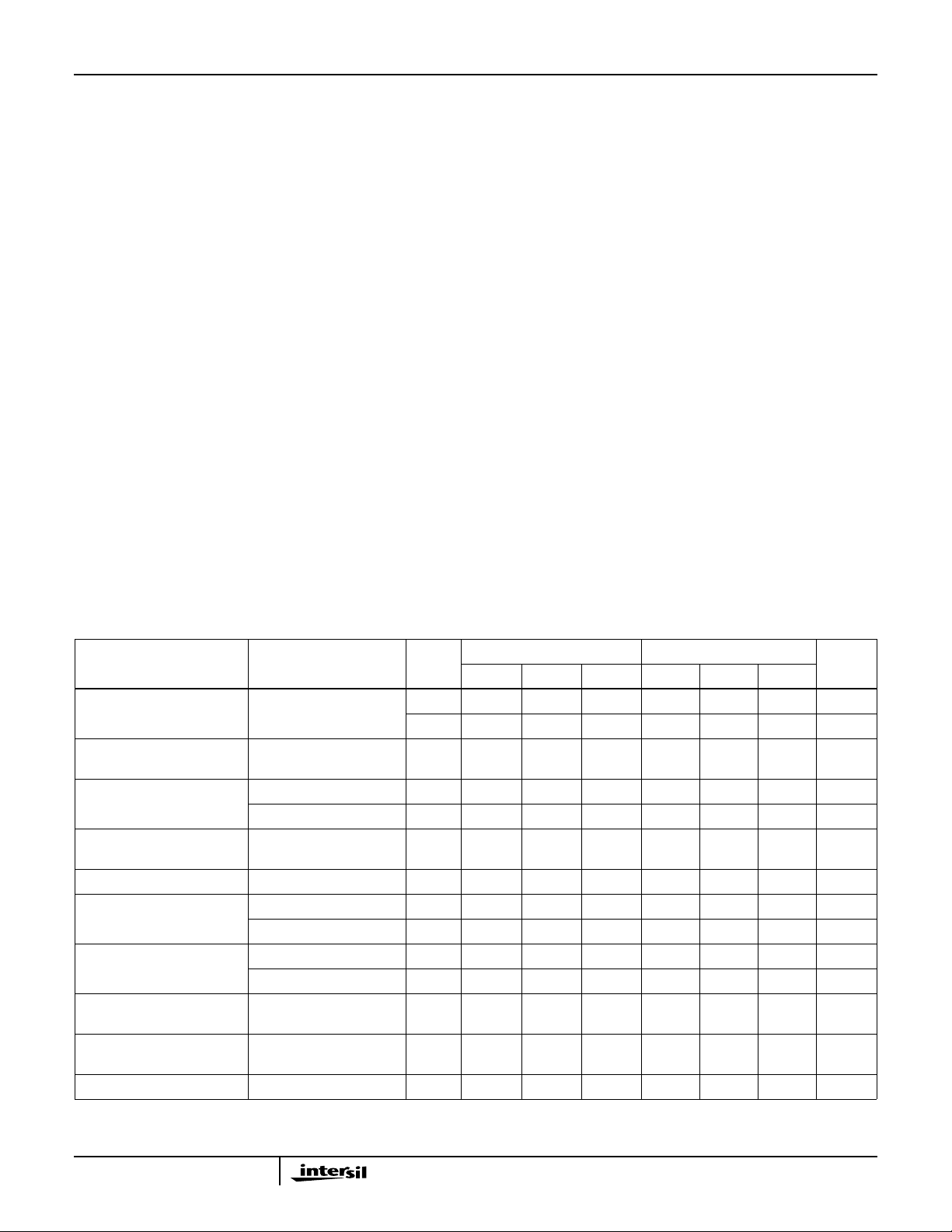
CA158, CA258, CA358 (PDIP, SOIC)
CA2904, LM358, LM2904 (PDIP)
OUTPUT (A)
INV. INPUT (A)
NON-INV. INPUT (A)
V-
TOP VIEW
1
2
3
4
V+
8
A
B
1
OUTPUT (B)
7
INV. INPUT (B)
6
NON-INV. INPUT (B)
5
CAUTION: These devices are sensitive to electrostatic discharge; follow proper IC Handling Procedures.
1-888-INTERSIL or 321-724-7143
| Copyright © Intersil Corporation 1999
CA158, CA158A, CA258, CA258A, CA358, CA358A, CA2904, LM358, LM2904
Absolute Maximum Ratings Thermal Information
Supply Voltage
CA2904, LM2904 . . . . . . . . . . . . . . . . . . . . . . . . . . . 26V or ±13V
Other Types . . . . . . . . . . . . . . . . . . . . . . . . . . . . . . . 32V or ±16V
Differential Input Voltage (All Types) . . . . . . . . . . . . . . . . . . . . . 32V
Input Voltage . . . . . . . . . . . . . . . . . . . . . . . . . . . . . . . . . .-0.3V to V+
Input Current (VI < -0.3V, Note 1) . . . . . . . . . . . . . . . . . . . . . . 50mA
Output Short Circuit Duration (V+ ≤ 15V, Note 2) . . . . . .Continuous
Operating Conditions
Temperature Range
CA158, CA158A. . . . . . . . . . . . . . . . . . . . . . . . . . -55oC to 125oC
CA258, . . . . . . . . . . . . . . . . . . . . . . . . . . . . . . . . . -25oC to 85oC
CA2904, LM2904 . . . . . . . . . . . . . . . . . . . . . . . . . . -40oC to 85oC
CA358, CA358A, LM358 . . . . . . . . . . . . . . . . . . . . . .0oC to 70oC
CAUTION: Stresses above those listed in “Absolute Maximum Ratings” may cause permanent damage to the device. This is a stress only rating and operation of the
device at these or any other conditions above those indicated in the operational sections of this specification is not implied.
NOTES:
1. This inputcurrent will onlyexist when thevoltage at anyofthe input leadsis driven negative.This current isdue to thecollectorbase junction ofthe
input PNPtransistorsbecoming forward biased andtherebyacting as input diodeclamps.In addition to thisdiode action, there is alsolateral NPN
parasitic transistor action on the IC chip. This transistor action can cause the output voltages of the amplifiers to go to the V+ voltage level (or to
ground foralarge overdrive) for thetimeduration that an input isdriven negative. This transistor actionis not destructive and normaloutput states
will re-establish when the input voltage, which was negative, again returns to a value greater than -0.3V.
2. The maximum output current is approximately 40mAindependentof the magnitude of V+. Continuous short circuits at V+ > 15V can cause
excessive power dissipation and eventual destruction. Short circuits from the output to V+ can cause overheating and eventual destruction of
the device. Destructive dissipation can result from simultaneous short circuits on both amplifiers.
3. θJA is measured with the component mounted on an evaluation PC board in free air.
Thermal Resistance (Typical, Note 3) θJA(oC/W) θJC(oC/W)
PDIP Package . . . . . . . . . . . . . . . . . . . 130 N/A
SOIC Package . . . . . . . . . . . . . . . . . . . 170 N/A
Can Package . . . . . . . . . . . . . . . . . . . . 155 67
Maximum Junction Temperature (Can Package). . . . . . . . . . .175oC
Maximum Junction Temperature (Plastic Package). . . . . . . . .150oC
Maximum Storage Temperature Range. . . . . . . . . . -65oC to 150oC
Maximum Lead Temperature (Soldering 10s) . . . . . . . . . . . . 300oC
(SOIC - Lead Tips Only)
Electrical Specifications Values Apply for Each Operational Amplifier. Supply Voltage V+ = 5V, V- = 0V,
Unless Otherwise Specified
TEMP
PARAMETER TEST CONDITIONS
Input Offset
Voltage (Note 6)
Average Input Offset Voltage
Drift
Input Common Mode Voltage
Range (Note 5)
Common Mode
Rejection Ratio
Power Supply Rejection Ratio DC 25 65 100 - 65 100 - dB
Input Bias
Current (Note 4)
Input Offset
Current
Average Input Offset Current
Drift
Large Signal Voltage Gain RL≥ 2kΩ, V+ = 15V (For
Output Voltage Swing RL = 2kΩ 25 0 - V+ -1.5 0 - V+ -1.5 V
RS = 0Ω Full - 7 15 - 7 20 µV/oC
V+ = 30V 25 0 - V+ -1.5 0 - V+ -1.5 V
V+ = 30V Full 0 - V+ -2 0 - V+ -2 V
DC 25 70 85 - 65 85 - dB
II+ or II- 25 - 20 50 - 45 100 nA
II+ or II- Full - 40 100 - 40 200 nA
II+ - II-25-210-530nA
II+ - II- Full - - 30 - - 75 nA
Large VO Swing)
(oC)
25 - 1 2 - 2 3 mV
Full - - 4 - - 5 mV
Full - 10 200 - 10 300 pA/oC
25 50 100 - 25 100 - kV/V
CA158A CA358A
UNITSMIN TYP MAX MIN TYP MAX
2
CA158, CA158A, CA258, CA258A, CA358, CA358A, CA2904, LM358, LM2904
Electrical Specifications Values Apply for Each Operational Amplifier. Supply Voltage V+ = 5V, V- = 0V,
Unless Otherwise Specified (Continued)
TEMP
PARAMETER TEST CONDITIONS
Output
Current
Short Circuit
Output Current (Note 2)
Crosstalk f = 1 to 20kHz
Total Supply Current RL = ∞ Full - 0.7 1.2 - 0.7 1.2 mA
NOTES:
4. Due to the PNPinput stage the direction of the input current is out of theIC.No loading change exists on the input lines because the currentis
essentially constant, independent of the state of the output.
5. The input signal voltageandthe input common mode voltage should not be allowed to go negative by morethan0.3V. The positive limit of the
common mode voltage range is V+ - 1.5V, but either or both inputs can go to +32V without damage.
6. VO = 1.4V, RS = 0Ω with V+ from 5V to 30V, and over the full input common mode voltage range (0V to V+ - 1.5V).
Source VI+ = +1V, VI- = 0V, V+ =
15V
Sink VI+ = 0V, VI- = 1V,
V+ = 15V
VI+ = 0V, VI- = 1V,
VO = 200mV
RL = 0Ω 25 - 40 60 - 40 60 mA
(Input Referred)
RL = ∞, V+ = 30V Full - 1.5 3 - 1.5 3 mA
(oC)
25 20 40 - 20 40 - mA
25 10 20 - 10 20 - mA
25 12 50 - 12 50 - µA
25 - -120 - - -120 - dB
CA158A CA358A
UNITSMIN TYP MAX MIN TYP MAX
Electrical Specifications Values Apply for Each Operational Amplifier. Supply Voltage V+ = 5V, V- = 0V,
Unless Otherwise Specified
TEST
PARAMETER
Input Offset
Voltage (Note 9)
Average Input Offset
Voltage Drift
Input Common Mode
Voltage Range (Note 8)
Common Mode
Rejection Ratio
Power Supply Rejection
Ratio
Input Bias
Current (Note 7)
Input Offset
Current
AverageInputOffset Current Drift
Large Signal Voltage
Gain
Output Voltage Swing RL = 2kΩ 25 0 - V+ -
CONDITIONS
RS = 0Ω Full - 7 - - 7 - - 7 - µV/oC
V+ = 30V 25 0 - V+ -
V+ = 30V Full 0 - V+ -2 0 - V+ -2 0 - V+ -2 V
DC 25 70 85 - 65 70 - 50 70 - dB
DC 25 65 100 - 65 100 - 50 100 - dB
II+ or II- 25 - 45 150 - 45 250 - 45 250 nA
II+ or II- Full - 40 300 - 40 500 - 40 500 nA
II+ - II- 25- 330- 550-550nA
II+ - II- Full - - 100 - - 150 - 45 200 nA
RL≥ 2kΩ, V+ = 15V
(For Large VO Swing)
TEMP
(oC)
25 - 2 5 - 2 7 - 2 7 mV
Full - - 7 - - 9 - - 10 mV
Full - 10 - - 10 - - 10 - pA/oC
25 50 100 - 25 100 - - 100 - kV/V
CA158, CA258 CA358, LM358 CA2904, LM2904
0 - V+ -
1.5
0 - V+ -
1.5
1.5
1.5
0 - V+ -
1.5
0 - V+ -
1.5
UNITSMIN TYP MAX MIN TYP MAX MIN TYP MAX
V
V
3
CA158, CA158A, CA258, CA258A, CA358, CA358A, CA2904, LM358, LM2904
Electrical Specifications Values Apply for Each Operational Amplifier. Supply Voltage V+ = 5V, V- = 0V,
Unless Otherwise Specified (Continued)
CA158, CA258 CA358, LM358 CA2904, LM2904
UNITSMIN TYP MAX MIN TYP MAX MIN TYP MAX
PARAMETER
Output
Current
TEST
CONDITIONS
Source VI+ = +1V, VI- = 0V,
V+ = 15V
Sink VI+ = 0V, VI- = 1V,
TEMP
(oC)
25 20 40 - 20 40 - 20 40 - mA
25 10 20 - 10 20 - 10 20 - mA
V+ = 15V
VI+ = 0V, VI- = 1V,
25 12 50 - 12 50 - - - - µA
VO = 200mV
Short Circuit
RL = 0Ω 25 - 40 60 - 40 60 - 40 60 mA
Output Current (Note 2)
Crosstalk f = 1 to 20kHz
25 - -120 - - -120 - - -120 - dB
(Input Referred)
Total Supply Current RL = ∞ Full - 0.7 1.2 - 0.7 1.2 - 0.7 1.2 mA
RL = ∞, V+ = 30V Full - 1.5 3 - 1.5 3 - 1.5 3 mA
NOTES:
7. Due to the PNPinput stage the direction of the input current is out of theIC.No loading change exists on the input lines because the currentis
essentially constant, independent of the state of the output.
8. The input signal voltageandthe input common mode voltage should not be allowed to go negative by morethan0.3V. The positive limit of the
common mode voltage range is V+ - 1.5V, but either or both inputs can go to +32V without damage.
9. VO = 1.4V, RS = 0Ω with V+ from 5V to 30V, and over the full input common mode voltage range (0V to V+ - 1.5V).
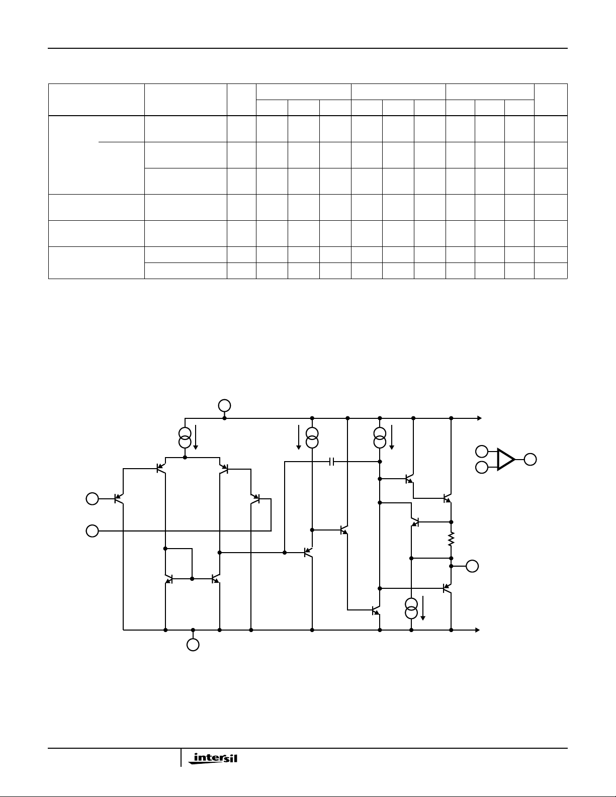
Schematic Diagram
2
-
INPUTS
3
+
Q
1
ONE OF TWO OPERATIONAL AMPLIFIERS
8
V+
TO 2
6µA4µA 100
Q
2
Q
8
Q
3
Q
4
Q
9
4
V-
Q
C
COMP
10
Q
11
µA
Q
5
Q
6
Q
7
R
SC
1
Q
13
Q
12
50µA
2
5
+
7
-
6
V
O
TO 2
4

CA158, CA158A, CA258, CA258A, CA358, CA358A, CA2904, LM358, LM2904
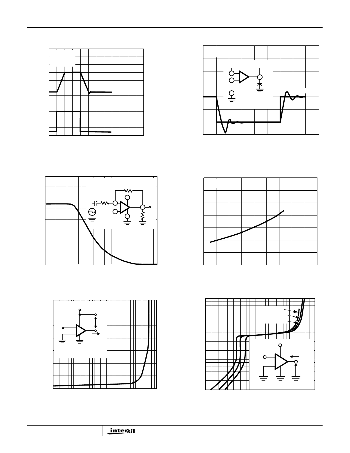
Typical Performance Curves
V
= 0V
ICR
60
15
10
INPUT VOLTAGE (V)
5
NEGATIVE
POSITIVE
0 5 10 15 20
SUPPLY VOLTAGE (V)
FIGURE 1. INPUT VOLTAGE RANGE vs SUPPLY VOLTAGE
V+
I
D
-
+
4
3
2
TA = 0oC TO 125oC
1
SUPPLY CURRENT DRAIN (mA)
0 5 10 15 20 25 30
POSITIVE SUPPLY VOLTAGE (V)
-55oC
mA
50
40
30
20
INPUT CURRENT (nA)
10
0
-75 -50 -25 0 25 50 75 100 125
FIGURE 2. INPUT CURRENT vs AMBIENT TEMPERATURE
120
100
80
60
40
20
COMMON MODE REJECTION RATION (dB)
0
100 1K 10K 100K 1M
V+ = 30V
15V
5V
TEMPERATURE (oC)
100
+
V
IN
100
100K
INPUT FREQUENCY (Hz)
+7.5V
-
+
-7.5V
DC
DC
100K
V
O
FIGURE 3. SUPPLY CURRENT DRAIN vs SUPPLY VOLTAGE FIGURE4. COMMON MODE REJECTION RATIO vs INPUT
FREQUENCY
TA = 25oC
150
125
100
75
50
25
OPEN LOOP VOLTAGE GAIN (dB)
0
0 10203040
POSITIVE SUPPLY VOLTAGE (V)
RL = 20kΩ
2kΩ
140
120
0.1µF
100
V
80
V+ = 10 TO 15V
60
40
OPEN-LOOP VOLTAGE GAIN (dB)
20
TA = -40 ≤ TA≤ 85oC
0
1 10 100 1K 10K 100K 1M 10M
I
V+ = 26V
FREQUENCY (Hz)
V+ / 2
10MΩ
V+
-
+
FIGURE 5. VOLTAGE GAIN vs SUPPLY VOLTAGE FIGURE 6. OPEN-LOOP FREQUENCY RESPONSE
5
V
O
CA158, CA158A, CA258, CA258A, CA358, CA358A, CA2904, LM358, LM2904
Typical Performance Curves (Continued)
TA = 25oC
V+ = 15V
= 2kΩ
R
L
4
3
2
1
INPUT VOLTAGE (V)
0
0 10203040
TIME (µs)
FIGURE 7. VOLTAGEFOLLOWER PULSERESPONSE
(LARGE SIGNAL)
20
15
10
TA = 25oC
V
1kΩ
+7V
I
100kΩ
-
+
+15V
4
3
2
1
0
V
2kΩ
O
OUTPUT VOLTAGE (V)
TA = 25oC
V+ = 30V
500
450
400
350
OUTPUT VOLTAGE (mV)
300
250
0123456789
OUTPUT
-
+
50pF
V
I
V
TIME (µs)
O
INPUT
FIGURE 8. VOLTAGEFOLLOWER PULSERESPONSE
(SMALL SIGNAL)
TA = 25oC
75
50
25
5
OUTPUT VOLTAGE SWING (V)
0
1K 10K 100K 1M
FREQUENCY (Hz)
INPUT CURRENT (nA)
0
010203040
POSITIVE SUPPLY VOLTAGE (V)
FIGURE 9. LARGE-SIGNAL FREQUENCY RESPONSE FIGURE 10. INPUT CURRENT vs SUPPLY VOLTAGE
8
7
V+ / 2
6
5
4
3
OUTPUT VOLTAGE (V)
(REFERENCED TO V+)
2
1
0.001 0.01 0.1 1 10 100
V+
V
+
-
INDEPENDENT OF V+
= 25oC
T
A
OUTPUT SOURCE CURRENT (mA)
O
+
I
O
FIGURE 11. OUTPUT SOURCE CURRENT CHARACTERISTICS
10
V+ = +5V
DC
V+ = +15 V
V+ = +30V
1
V+ / 2
0.1
OUTPUT VOLTAGE (V)
0.01
0.001 0.01 0.1 1 10 100
OUTPUT SINK CURRENT (mA)
T
A
DC
DC
V+
-
+
= 25oC
FIGURE 12. OUTPUT SINK CURRENT CHARACTERISTICS
I
O
V
O
6
CA158, CA158A, CA258, CA258A, CA358, CA358A, CA2904, LM358, LM2904
Typical Performance Curves (Continued)
70
V+ = 15V
60
50
40
30
20
10
OUTPUT SOURCE CURRENT (mA)
0
-75 -50 -25 0 25 50 75 100 125
FIGURE 13. OUTPUT CURRENT vs AMBIENT TEMPERATURE
Metallization Mask Layout
72
70
TEMPERATURE (oC)
666050403020100
60
50
40
30
20
10
0
4 - 10
(0.102 - 0.254)
63 - 71
(1.600 - 1.803)
69 - 77
(1.753 - 1.956)
Dimensions in parentheses are in millimeters and derived
from the basic inch dimensions as indicated. Grid graduations are in mils (10-3 inch).
The photographs and dimensions represent a chip when it
is part of the wafer. When the wafer is cut into chips, the
cleavage angles are 57oinstead of 90owith respect to the
face ofthechip. Therefore, theisolatedchip is actually 7mils
(0.17mm) larger in both dimensions.
All Intersil semiconductor products are manufactured, assembled and tested under ISO9000 quality systems certification.
Intersil semiconductor products are sold by description only. Intersil Corporation reserves the right to make changes in circuit design and/or specifications at anytime without notice. Accordingly, the reader is cautioned to verify that data sheets are current before placing orders. Information furnished by Intersil is believed to be accurate and
reliable. However,no responsibility is assumed by Intersil or its subsidiaries forits use; nor for any infringements of patents or other rights of third parties which may result
from its use. No license is granted by implication or otherwise under any patent or patent rights of Intersil or its subsidiaries.
For information regarding Intersil Corporation and its products, see web site http://www.intersil.com
7
 Loading...