JANSR2N7294
Formerly FRF250R4
June 1998
Features
• 23A, 200V, r
• Total Dose
- Meets Pre-RAD Specifications to 100K RAD (Si)
• Dose Rate
- Typically Survives 3E9 RAD (Si)/s at 80% BV
- Typically Survives 2E12 if Current Limited to I
• Photo Current
- 12nA Per-RAD(Si)/s Typically
• Neutron
- Maintain Pre-RAD Specifications
for 1E13 Neutrons/cm
- Usable to 1E14 Neutrons/cm
Ordering Information
PART NUMBER PACKAGE BRAND
DS(ON)
= 0.115Ω
2
2
DSS
DM
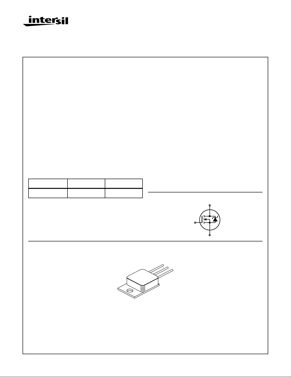
23A, 200V, 0.115 Ohm, Rad Hard,
N-Channel Power MOSFET
Description
The Intersil Corporation has designed a series of SECOND
GENERATION hardened power MOSFETs of both N-Channel and P-Channel enhancement types with ratings from
100V to 500V, 1A to 60A, and on resistance as low as
25mΩ. Total dose hardness is offered at 100K RAD (Si) and
1000K RAD (Si) with neutron hardness ranging from 1E13
for 500V product to 1E14 for 100V product. Dose rate hardness (GAMMA DOT) exists for rates to 1E9 without current
limiting and 2E12 with current limiting.
This MOSFET is an enhancement-mode silicon-gate power
field effect transistor of the vertical DMOS (VDMOS) structure. It is specially designed and processed to exhibit minimal characteristic changes to total dose (GAMMA) and
neutron (n
also directed to enhance survival to dose rate (GAMMA
DOT) exposure.
Also availableat other radiation and screening levels. See us
on the web, Intersil’ home page: http://www.intersil.com.
Contact your local Intersil Sales Office for additional information.
o
) exposures. Design and processing efforts are
JANSR2N7294 TO-254AA JANSR2N7294
Die family TA17652.
MIL-PRF-19500/605.
Package
CAUTION: Beryllia Warning per MIL-S-19500
Symbol
TO-254AA
G
S
D
refer to package specifications.
D
G
S
CAUTION: These devices are sensitive to electrostatic discharge; follow proper IC Handling Procedures.
1-888-INTERSIL or 321-724-7143 | Copyright © Intersil Corporation 2000.
2-23
File Number 4292.1

JANSR2N7294
Absolute Maximum Ratings T
= 25oC, Unless Otherwise Specified
C
JANSR2N7294 UNITS
Drain to Source Voltage . . . . . . . . . . . . . . . . . . . . . . . . . . . . . . . . . . . . . . . . . . . . . . . . . . . . .V
Drain to Gate Voltage (RGS = 20kΩ) . . . . . . . . . . . . . . . . . . . . . . . . . . . . . . . . . . . . . . . . . V
DS
DGR
200 V
200 V
Continuous Drain Current
TC = 25oC. . . . . . . . . . . . . . . . . . . . . . . . . . . . . . . . . . . . . . . . . . . . . . . . . . . . . . . . . . . . . . . I
TC = 100oC. . . . . . . . . . . . . . . . . . . . . . . . . . . . . . . . . . . . . . . . . . . . . . . . . . . . . . . . . . . . . . I
Pulsed Drain Current . . . . . . . . . . . . . . . . . . . . . . . . . . . . . . . . . . . . . . . . . . . . . . . . . . . . . . . I
Gate to Source Voltage . . . . . . . . . . . . . . . . . . . . . . . . . . . . . . . . . . . . . . . . . . . . . . . . . . . . .V
D
D
DM
GS
23 A
15 A
69 A
±20 V
Maximum Power Dissipation
TC = 25oC. . . . . . . . . . . . . . . . . . . . . . . . . . . . . . . . . . . . . . . . . . . . . . . . . . . . . . . . . . . . . . .P
TC = 100oC. . . . . . . . . . . . . . . . . . . . . . . . . . . . . . . . . . . . . . . . . . . . . . . . . . . . . . . . . . . . . .P
T
T
125 W
50 W
Linear Derating Factor . . . . . . . . . . . . . . . . . . . . . . . . . . . . . . . . . . . . . . . . . . . . . . . . . . . . . . . 1.00 W/oC
Single Pulsed Avalanche Current, L = 100µH, (See Test Figure). . . . . . . . . . . . . . . . . . . . . . I
Continuous Source Current (Body Diode) . . . . . . . . . . . . . . . . . . . . . . . . . . . . . . . . . . . . . . . . I
Pulsed Source Current (Body Diode). . . . . . . . . . . . . . . . . . . . . . . . . . . . . . . . . . . . . . . . . . . I
Operating and Storage Temperature . . . . . . . . . . . . . . . . . . . . . . . . . . . . . . . . . . . . . . .TJ,T
STG
Lead Temperature (During Soldering) . . . . . . . . . . . . . . . . . . . . . . . . . . . . . . . . . . . . . . . . . . . T
AS
S
SM
L
69 A
23 A
69 A
-55 to 150
300
o
C
o
C
(Distance >0.063in (1.6mm) from Case, 10s Max)
Weight (Typical) . . . . . . . . . . . . . . . . . . . . . . . . . . . . . . . . . . . . . . . . . . . . . . . . . . . . . . . . . . . . . . 9.3 g
CAUTION: Stresses above those listed in “Absolute Maximum Ratings” may cause permanent damage to the device. This is a stress only rating and operation
of the device at these or any other conditions above those indicated in the operational sections of this specification is not implied.
Electrical Specifications T
= 25oC, Unless Otherwise Specified
C
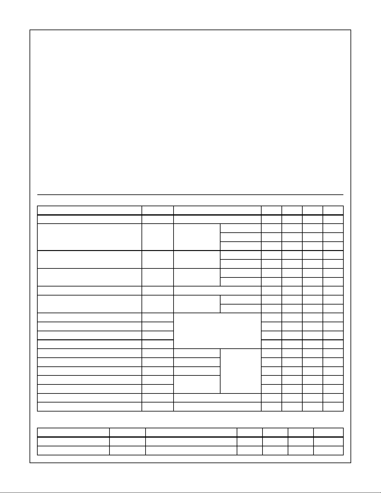
PARAMETER SYMBOL TEST CONDITIONS MIN TYP MAX UNITS
Drain to Source Breakdown Voltage BV
Gate Threshold Voltage V
GS(TH)VGS
Zero Gate Voltage Drain Current I
Gate to Source Leakage Current I
Drain to Source On-State Voltage V
Drain to Source On Resistance r
Turn-On Delay Time t
DS(ON)VGS
DS(ON)ID
d(ON)
Rise Time t
Turn-Off Delay Time t
d(OFF)
Fall Time t
Total Gate Charge (Not on slash sheet) Q
g(TOT)VGS
Gate Charge at 10V Q
Threshold Gate Charge (Not on slash sheet) Q
Gate Charge Source Q
Gate Charge Drain Q
Thermal Resistance Junction to Case R
Thermal Resistance Junction to Ambient R
DSSID
DSS
GSS
r
f
g(10)
g(TH)
gs
gd
JC
θ
JA
θ
= 1mA, VGS = 0V 200 - - V
= VDS,
ID = 1mA
VDS = 160V,
VGS = 0V
TC = -55oC - - 5.0 V
= 25oC 2.0 - 4.0 V
T
C
= 125oC 1.0 - - V
T
C
TC = 25oC--25µA
= 125oC - - 250 µA
T
C
VGS = ±20V TC = 25oC - - 100 nA
= 125oC - - 200 nA
T
C
= 10V, ID = 23A - - 2.78 V
= 15A,
VGS = 10V
VDD = 100V, ID = 23A,
RL = 4.35Ω, VGS = 10V,
RGS = 25Ω
TC = 25oC - - 0.115 Ω
= 125oC - - 0.253 Ω
T
C
- - 156 ns
- - 510 ns
- - 574 ns
- - 280 ns
= 0V to 20V VDD = 100V,
VGS = 0V to 10V - - 298 nC
ID = 23A
- - 558 nC
VGS = 0V to 2V - - 20 nC
- - 66 nC
- - 144 nC
- - 1.0
o
C/W
--48oC/W
Source to Drain Diode Specifications
PARAMETER SYMBOL TEST CONDITIONS MIN TYP MAX UNITS
Forward Voltage V
Reverse Recovery Time t
SD
rr
ISD = 25A 0.6 - 1.8 V
ISD = 25A, dISD/dt = 100A/µs - - 1700 ns
2-24

JANSR2N7294
Electrical Specifications up to 100K RAD T
= 25oC, Unless Otherwise Specified
C
PARAMETER SYMBOL TEST CONDITIONS MIN MAX UNITS
Drainto Source BreakdownVolts (Note 3) BV
Gate to Source Threshold Volts (Note 3) V
Gate to Body Leakage (Notes 2, 3) I
Zero Gate Leakage (Note 3) I
Drain to Source On-State Volts (Notes 1, 3) V
Drain to Source On Resistance (Notes 1, 3) r
DS(ON)
DSS
GS(TH)
GSS
DSS
DS(ON)
VGS = 0, ID = 1mA 200 - V
VGS = VDS, ID = 1mA 2.0 4.0 V
VGS = ±20V, VDS = 0V - 100 nA
VGS = 0, VDS = 160V - 25 µA
VGS = 10V, ID = 23A - 2.78 V
VGS = 10V, ID = 15A - 0.115 Ω
NOTES:
1. Pulse test, 300µs Max.
2. Absolute value.
3. Insitu Gamma bias must be sampled for both VGS = 10V, VDS = 0V and VGS = 0V, VDS = 80% BV
Typical Performance Curves Unless Otherwise Specified
28
24
100
DSS
.
TC = 25oC
20
16
12
, DRAIN (A)
D
I
8
4
0
TC, CASE TEMPERATURE (oC)
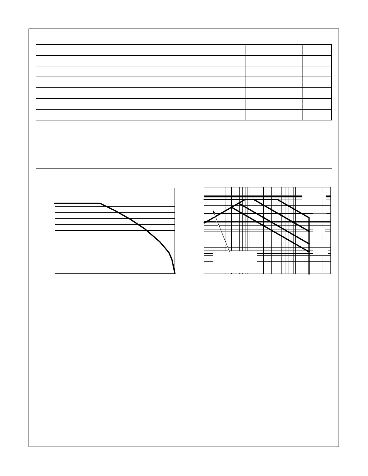
FIGURE 1. MAXIMUM CONTINUOUS DRAIN CURRENT vs
CASE TEMPERATURE
10
1
, DRAIN CURRENT (A)
D
I
150100500-50
0.1
OPERATION IN THIS
AREA MAY BE
LIMITED BY r
1
DS(ON)
10
, DRAIN TO SOURCE VOLTAGE (V)
V
DS
100
100µs
1ms
10ms
100ms
FIGURE 2. FORWARD BIAS SAFE OPERATING AREA
2-25
 Loading...