

Page 1

Application Note 1664
ISL97683 LED Driver Evaluation Board User Manual
Introduction
The ISL97683 Evaluation Board provides a complete testing
platform for ISL97683, a three channel LED driver. Please
refer to the product datasheet for detailed information,
including pinout, pin function descriptions, electrical
specifications and applications related information.
Instructions
Please follow the steps described below to start your
evaluation.
1. Set Switch #1 and Switch #2 (SW1 and SW2) to position 3
(left side).
2. For the enable control jumper, JP1, set the shunt to the
“ON” position (right side) to connect the EN pin to VIN.
When the shunt is in the “OFF” position, it will disable the
chip by pulling the EN pin to ground.
3. Connect JP14 so the VIN pin is connected to PVIN.
4. For JP20, connect the shunt to the upper position.
5. Connect WR and JP2-JP6.
6. Apply 1.5V~5.5V PWM signal between the PWMI pin and
AGND.
7. Apply 4V~26.5V between PVIN and PGND and the LEDs
should be lit. You may start the evaluation.
Note
:
• In Step #1 above, the SW1, SW2 position can be adjusted to
different positions for different configurations. Details are
provided in the following:
• LED dimming frequency and duty cycle
1. As mentioned in Step #4, when the shunt on JP20 is
connected to the upper position and the FPWM/DPWM pin
is connected to VDC, the device enters direct PWM mode,
which means both the LED dimming frequency and the
duty cycle are synchronized with the external PWM signal
applied on the PWMI pin.
2. When the shunt on JP20 is connected to the lower position,
the FPWM/DPWM pin is connected to a resistor. Under
such conditions, the LED dimming frequency of the chip is
programmed by the resistance connected on the
FPWM/DPWM pin per the following equation:
FPWM Hz()12.4
7
×10 R_FPWM Ω()⁄=
(EQ. 2)
The duty cycle is still modulated by the external PWM signal
applied on the PWMI pin. On board, a potentiometer R11
and a few other resistors are provided for easily adjusting
the LED dimming frequency under such configuration.
TABLE 1.
SW1
POSITION
1 1 LX switching frequency = 600kHz, PFM
3 3 LX switching frequency = 1MHz, PFM
3 1 LX switching frequency = 600kHz, No PFM
1 3 LX switching frequency = 1MHz, No PFM
SW2
POSITION DESCRIPTION
CH1-CH3
CH1-CH3
CH1-CH3
CH1-CH3
• The LED maximum DC current adjustment
For each channel, the maximum DC current is set by
resistance connected to the RSET pin. The current for each
channel can be calculated as follows:
I_LED(mA) 402 RS E T⁄ kΩ〈〉=
On the board, a potentiometer R5 and a few other resistors
are provided for easily adjusting the LED maximum DC
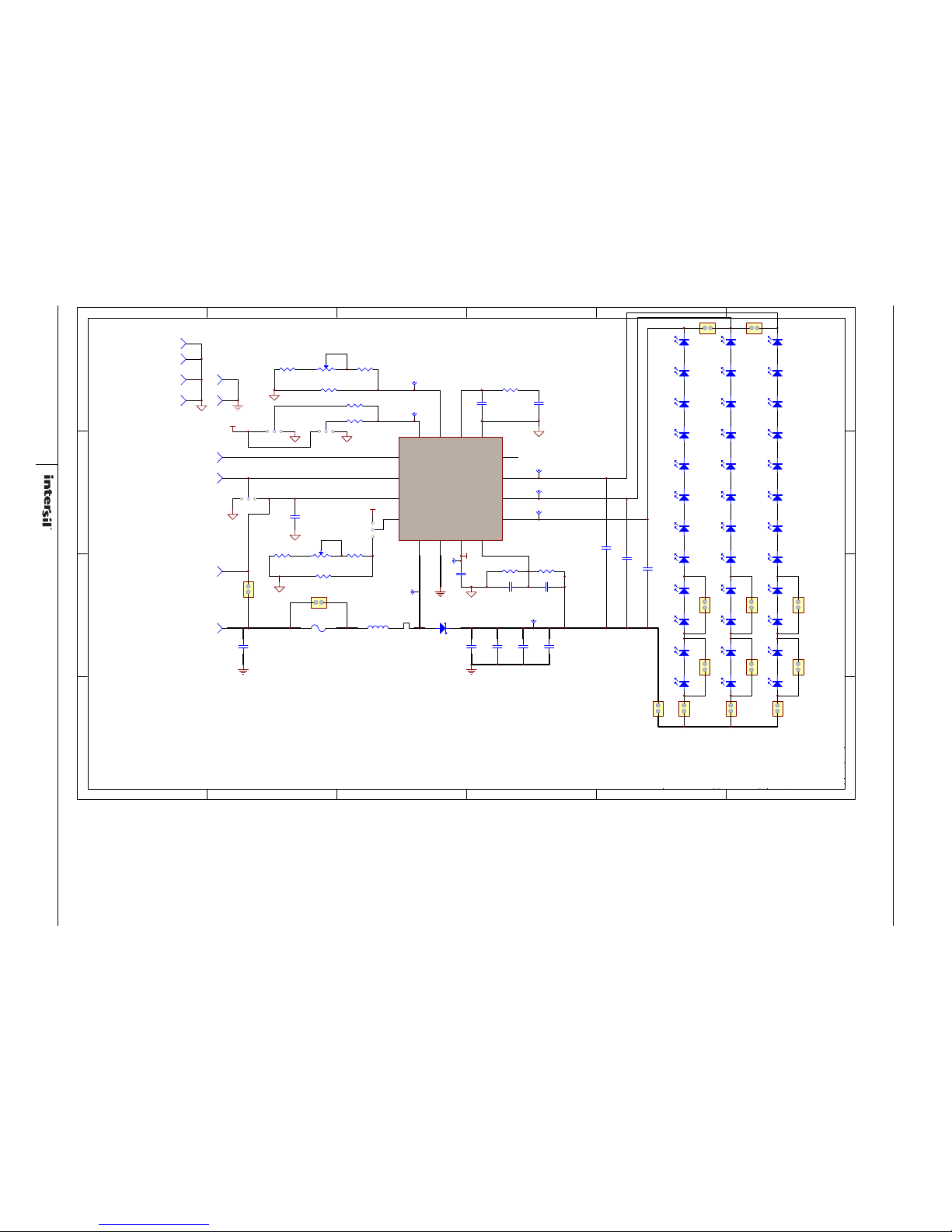
current; please refer to the evaluation board schematic on
page 2 for more details.
(EQ. 1)
December 13, 2011
AN1664.0
1
CAUTION: These devices are sensitive to electrostatic discharge; follow proper IC Handling Procedures.
1-888-INTERSIL or 1-888-468-3774
Intersil (and design) is a trademark owned by Intersil Corporation or one of its subsidiaries.
All other trademarks mentioned are the property of their respective owners.
|Copyright Intersil Americas Inc. 2011. All Rights Reserved
Page 2
Application Note 1664
2
AN1664.0
December 13, 2011
1 2 3 4 56
A
B
C
D
6
54321
D
C
B
A
Title
Number RevisionSize
B
Date: 10-Oct-2011 Sheet of
File: C:\ISL97682_3_4\ISL97682EVAL1Z_RevA.ddbDrawn By:
L1
15uH
D1
PMEG6030
1 3
2
SW1
1 3
2
SW2
R1
150k
R2
100k
When
SW1=SW2=1: Fsw=1.2MHz, WITH phase shift
SW1=SW2=3: Fsw=600KHz, WITH phase shift
SW1=1, SW2=3: Fsw=1 .2MHz, WITHOUT phase sh ift
SW1=3, SW2=1: Fsw=6 00KHz, WITHOUT phase sh ift
C1
10uF/50V
C2
0.1uF/50V
P1
PVIN
C4
1uF/16V
P3
EN
P4
PWMI
VDC
C5
4.7uF/50VC64.7uF/50VC7NCC8NC
LED1 LED13 LED25
LED2 LED14 LED26
LED3 LED15 LED27
LED4 LED16 LED28
LED5 LED17 LED29
LED6 LED18 LED30
LED7 LED19 LED31
LED8 LED20 LED32
LED9 LED21 LED33
LED10 LED22 LED34
LED11 LED23 LED35
LED12 LED24 LED36
JP2
I_OUT
JP3 JP4 JP5
R4
10k
R3
357k
C10
3.3nF/50VC9100pF/50V
JP7 JP8 JP9
JP11 JP12
C13
1nF/50V
C12
1nF/50V
C11
1nF/50V
R5
1M
R6
0
R7
Open
R8
5k
R9
10k
C15
8.2nF
C3
33pF
TP1
LX
TP2
VOUT
TP3
CH1
TP4
CH2
TP5
CH3
TP7
VDC
P5
AGND
P6
AGND
P7
AGND
P8
AGND
P9
PGND
P10
PGND
2-layer board. Connect top layer PGND and bottom
layer AGND at one single point through the via on
the thermal pad under the chip.
F1
2A Fuse
JP14
R11
100k
R10
0
R13
Open
R12
27k
JP15 JP16 JP17
ISL97683EVAL1Z
Rev. A
EN can be connected in the following ways to
enable/disable the device:
(1) Connected it to VIN directly on JP1 to enable
(2) Connected it to GND directly on JP1 to disable
(3) Directly apply external voltage on P3(EN) to
enable/disable the device without putting shunt on JP1.
JP2: For measuring total output current
JP3-JP6: For measuring current on CH1-CH4 respectively
JP7-JP10, JP13-JP16: For easy configuration of 8x LED or 10x
LED per string
JP19
12
WR
TP8
RSET
TP9
FSW/PHS
P2
VIN
VDC
1 3
2
JP1
13
2
JP20
VDC
NC
16
AGND
1
COMP
2
RSET
3
FSW
4
PWMI
5
EN
6
VIN
7
FPWN/DPWM
8
LX9PGND10VDC11OVP
12
CH1
13
CH2
14
CH3
15
ISL97683
U1
XAL6060-153MEB
FIGURE 1. EVALUATION BOARD SCHEMATIC
Page 3
Application Note 1664
3
AN1664.0
December 13, 2011
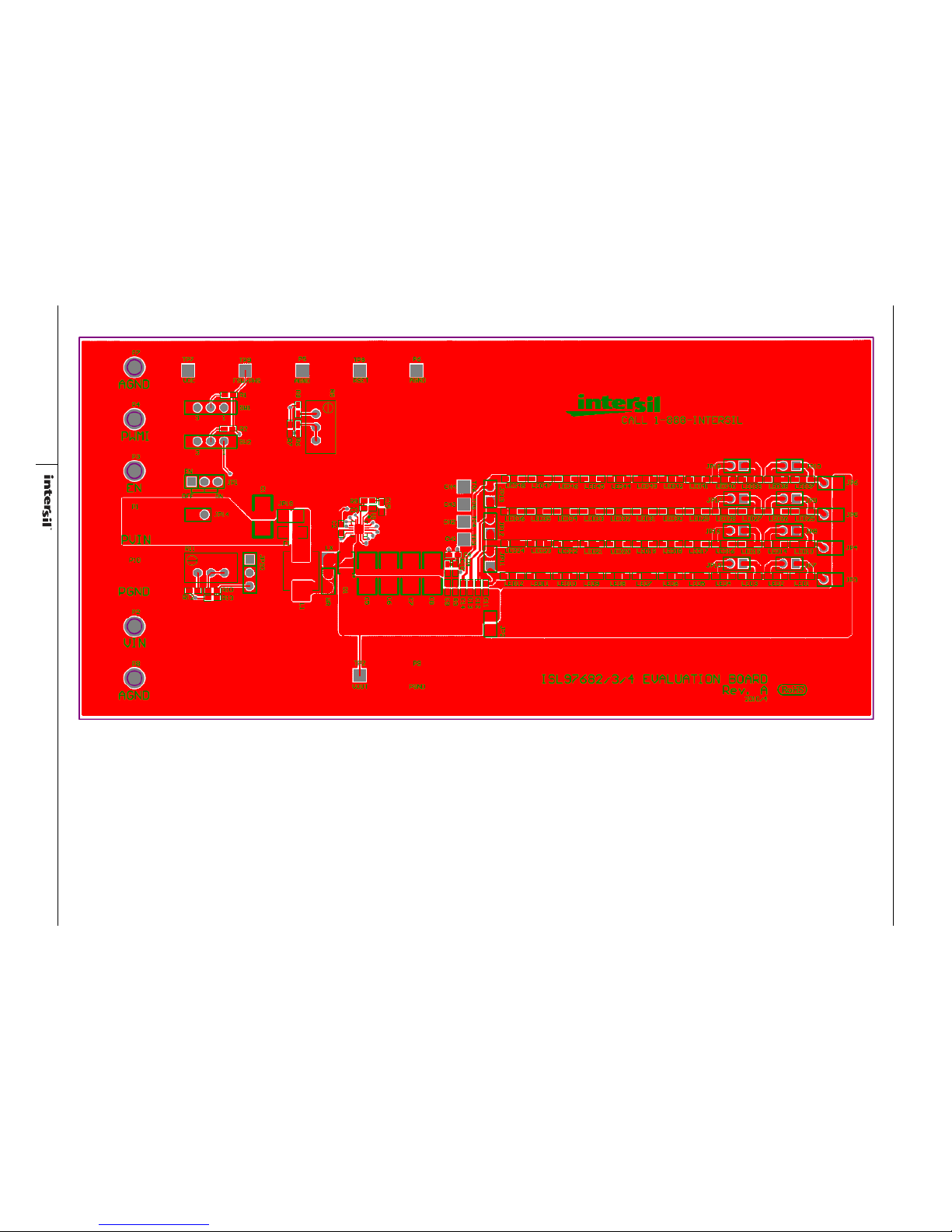
PCB Layout
FIGURE 2. TOP SILKSCREEN LAYER AND TOP LAYER
Page 4
Application Note 1664
4
AN1664.0
December 13, 2011
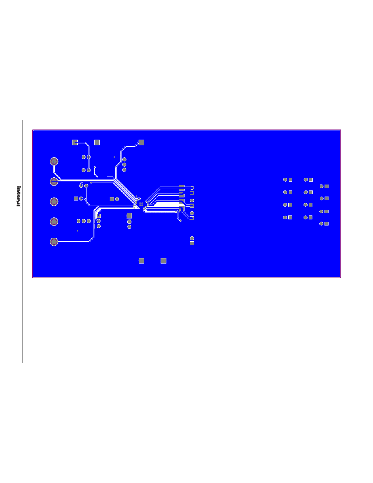
FIGURE 3. BOTTOM LAYER
PCB Layout (Continued)
Page 5

Application Note 1664
Bill of Materials (BOM)
DESIGNATOR PART TYPE FOOTPRINT PART MANUFACTURER/NUMBER
R1 150k 603 1% SMD Resistor
R2 100k 603 General purpose
R3 357k 603
R4 10k 603
R5 1M VRES
R6 0 603
R7 Open 603
R8 5k 603
R9 10k 603
R10 0 603
R11 100k VRES
R12 27k 603
R13 Open 603
L1 15µH CoilCraft, XAL6060-153MEB
D1 PMEG6030 SOD128 NXP SEMICONDUCTOR
C1 10µF/50V 1210 General purpose
C2 0.1µF/50V 603 Ceramic X5R/X7R capacitors
C3 33pF 603
C4 1µF/16V 603
C5 4.7µF/50V 1210 Murata, GRM32ER71H475KA88L
C6 4.7µF/50V 1210
C7 Place Holder 1210 Not Populated
C8 Place Holder 1210
C9 100pF/50V 603 General purpose
C10 3.6nF/50V 603 Ceramic X5R/X7R capacitors
C11 1nF/50V 603
C12 1nF/50V 603
C13 1nF/50V 603
C14 Place Holder 603
C15 8.2nF 603
F1 2A Fuse 1206 Bel Fuse Inc, C1Q 2
U1 QFN16 3MM Intersil, ISL97682/3/4
JP2-JP19 JUMPER-2PIN JUMPER-2PIN FCI
WR JUMPER-2PIN JUMPER-2PIN 68000-236HLF-1x2
JP1 JUMPER-3PIN JUMPER-3PIN FCI
JP20 JUMPER-3PIN JUMPER-3PIN 68000-236HLF-1x3
LED1-LED48 LED-SMT LW_Y87C
TP1 LX TEST POINT Keystone Electronics
TP2 VOUT TEST POINT 5010
5
AN1664.0
December 13, 2011
Page 6

Application Note 1664
Bill of Materials (BOM)
DESIGNATOR PART TYPE FOOTPRINT PART MANUFACTURER/NUMBER
TP3 CH1 TEST POINT
TP4 CH2 TEST POINT
TP5 CH3 TEST POINT
TP6 CH4 TEST POINT
TP7 VDC TEST POINT
TP8 RSET TEST POINT
TP9 FSW/PHS TEST POINT
P5 AGND TEST POINT Keystone Electronics
P6 AGND TEST POINT 5011
P9 PGND TEST POINT
P1 PVIN POWERPOST Mill Max
P2 VIN POWERPOST 3156-1-00-00-00-00-08-0
P3 EN POWERPOST
P4 PWMI POWERPOST
P7 AGND POWERPOST
P8 AGND POWERPOST
P10 PGND POWERPOST
SW2 SPDT SWITCH-SLIDE-SPDT EAO
SW1 SPDT SWITCH-SLIDE-SPDT 09.03201.02
Intersil Corporation reserves the right to make changes in circuit design, software and/or specifications at any time without notice. Accordingly, the reader is
cautioned to verify that the Application Note or Technical Brief is current before proceeding.
For information regarding Intersil Corporation and its products, see www.intersil.com
6
AN1664.0
December 13, 2011
 Loading...