

Page 1
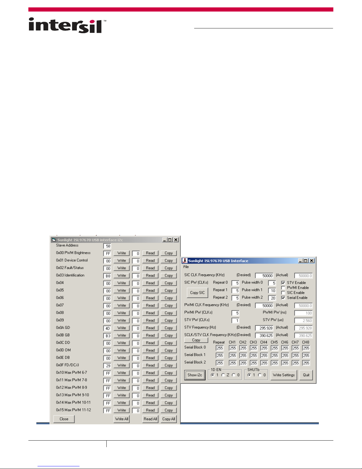
FIGURE 1. EXAMPLE OF GUI INTERFACE
Application Note 1634
ISL97671A, ISL97672A Evaluation Board Quick Start
Guide
Description
This quick start guide pertains to the ISL97671A, ISL97672A
Evaluation Board Rev A-1 (Oct 2011). This board comes
populated with 78 LED’s in 6P13S configuration to simplify
evaluation and testing. In the case of the ISL97671A
evaluation board, please install the Sunlight ISL97670 GUI,
which will be used to control these parts via I
that the slave address on the ISL97671A is hexadecimal 58;
see Figure 1. Please refer to respective the ISL97671A or
ISL97672A section for jumper settings and power up
instructions.
2
C. Please note
ISL97671A
1. ISL97671A LED strings can be configured in 6P13S,
6P12S, 6P11S, and 6P10S with different LED jumper
settings, as shown in Table 1.
2. Connect WR, JP_OUTPUT, and JPCH0-JPCH5. Leave JP1
open to use external fault protection FET (Q1).
3. For current LED configuration, connect jumper JP1A to the
left and connect the power supply on J99 (IC_VIN) to deliver
VIN to the IC. When there is less LED in each string and
VOUT is lower than 28V, IC_VIN can be configured as the
bootstrap generated from the boost output by connecting
the jumper JP1A to the right
4. IC Enable is shorted to VIN by connecting jumper JP2A to
the right, thereby shorting jumper JP2A to the left so that
the EN is driven by J98(EN)
2
5. VLOGIC level for I
connecting jumper JP3A to the right. VLOGIC can be driven
from J97 (VLOGIC) by shorting jumper JP3A to the left.
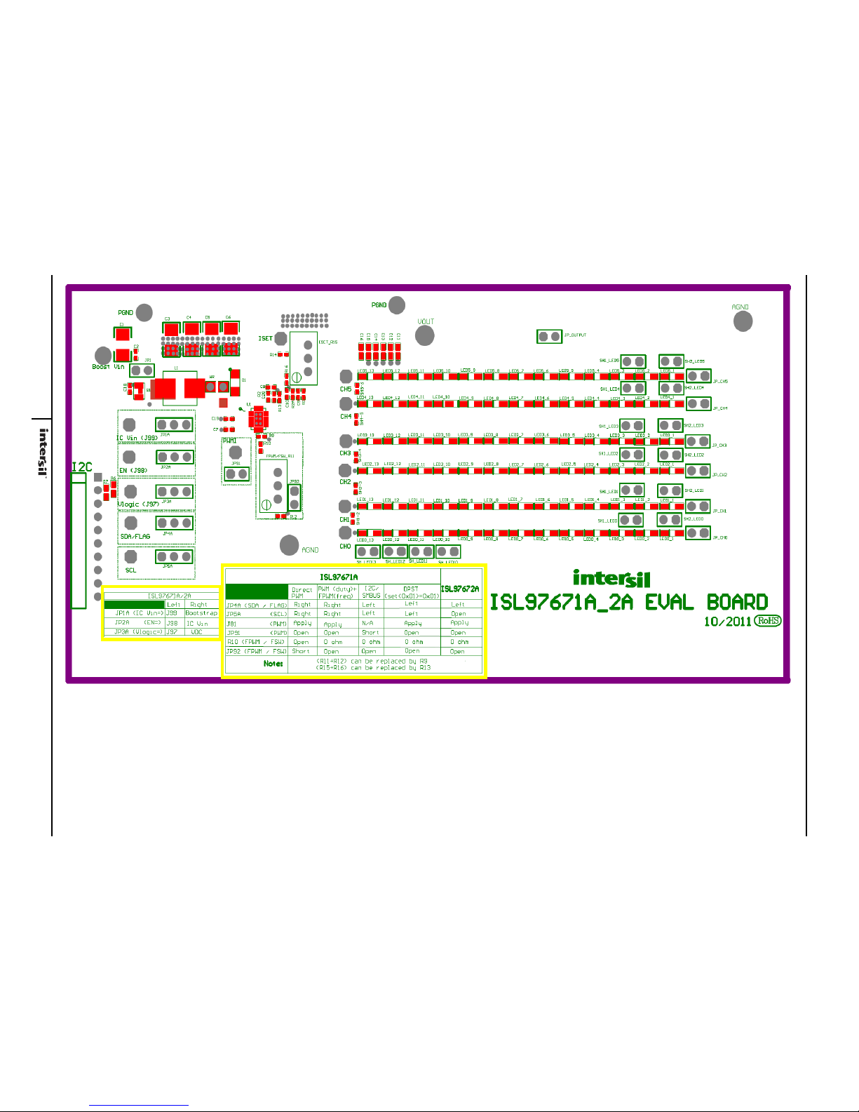
6. The configuration of VIN (JP1A), EN (JP2A), and VLOGIC
(JP3A) can be quickly found by referring to the table printed
on the evaluation board, as shown in Figure 3.
7. There are 4 different operation modes for ISL97671A. The
setting for each mode is shown on the other table printed
on the evaluation board, as shown in Figure 3.
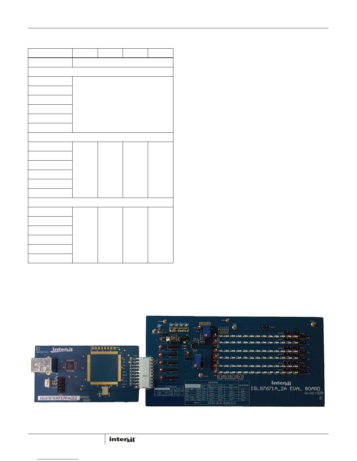
8. For I2C/SMBUS and DPST mode, connect the I2C interface
board to the ISL97671A evaluation board, as shown in
Figure 2.
9. For I2C/SMBUS and DPST mode, in order to enable the
board, write a hex 58 for Slave Address and write a hex 05
in register 01; writing a hex 01 in register 01 will enable
DPST (see data sheet for more details); writing a hex 03 in
register 01 will allow PWM dimming only.
C can be generated from VDC by
June 13, 2012
AN1634.1
1
1-888-INTERSIL or 1-888-468-3774
CAUTION: These devices are sensitive to electrostatic discharge; follow proper IC Handling Procedures.
| Intersil (and design) is a trademark owned by Intersil Corporation or one of its subsidiaries.
All other trademarks mentioned are the property of their respective owners.
Copyright Intersil Americas Inc. 2012. All Rights Reserved
Page 2
Application Note 1634
(EQ. 1)
IL E D 410.5 R15 R 16+()410.5 R13⁄=⁄=
(EQ. 2)
F
PWM
6.66 107R11 R12+()⁄×=
(EQ. 3)
F
sw
510
10
×()R11 R12+()⁄=
FIGURE 2. I2C INTERFACE BOARD CONNECTED TO THE ISL97671A EVALUATION BOARD
TABLE 1. LED STRINGS CONFIGURATIONS WITH DIFFERENT JUMPER
SETTINGS
LED CONFIGUATRION 6P13S 6P12S 6P11S 6P10S
JP_OUTPUT Short
JP_CH0
JP_CH1
JP_CH2
JP_CH3
JP_CH4
JP_CH5
SH1_LED0
SH1_LED1
SH1_LED2
SH1_LED3
SH1_LED4
SH1_LED5
SH2_LED0
SH2_LED1
SH2_LED2
SH2_LED3
SH2_LED4
SH2_LED5
Open Short Open Short
Open Open Short Short
Short
10. The LED current can be programmed by varying POT R15
using the following equation:
The measured current divided by six is the LED current per
channel. For example, 120mA measured current will correspond
to 20mA/channel.
11. The PWM dimming frequency can be adjusted by varying pot
R11 using the following equation:
ISL97672A
1. ISL 97672A LED strings can be configured in 6P13S, 6P12S,
6P11S, and 6P10S with different LED jumper settings, as
shown in Table 1.
2. Connect WR, JP_OUTPUT, and JPCH0-JPCH5. Leave JP1 open
to use external fault protection FET (Q1).
3. For current LED configuration, connect jumper JP1A to the left
and connect the power supply on J99 (IC_VIN) to deliver VIN to
th e IC. W hen t here i s less LED i n each strin g and VOUT is lo wer
than 28V, IC VIN can be configured as the bootstrap
generated from the boost output by connecting the jumper
JP1A to the right.
4. IC Enable is shorted to VIN by connecting jumper JP2A to the
right, thereby shorting jumper JP2A to the left so that EN is
driven by J98 (EN).
5. VLOGIC level can be generated from VDC by connecting
jumper JP3A to the right. VLOGIC can be driven from J97
(VLOGIC) by shorting jumper JP3A to the left.
6. Configuration of VIN (JP1A), EN (JP2A), and VLOGIC (JP3A)
can be quickly found by referring to the table printed on the
evaluation board, as shown in Figure 3.
7. There is only one operation mode for ISL97672A, and the
settings for JP4A, JP5A, J81, JP91, R10, and JP92 need to
follow the table printed on the evaluation board, as shown in
Figure 3.
8. The boost switching frequency can be adjusted by varying pot
R11 using the following equation:
2
AN1634.1
Page 3
Application Note 1634
3
AN1634.1
FIGURE 3. SETTINGS OF IC VIN, ENABLE, AND VLOGIC ARE S HOWN ON PCB IN YEL LOW RECTANGE ON THE LEF T-HAND SIDE. CONFIGURATIONS OF 4 DIFFERENT OPERATION MODES ARE
LISTED ON PCB IN YELLOW RECTANGE ON THE RIGHT-HAND SIDE.
Page 4
Application Note 1634
4
AN1634.1
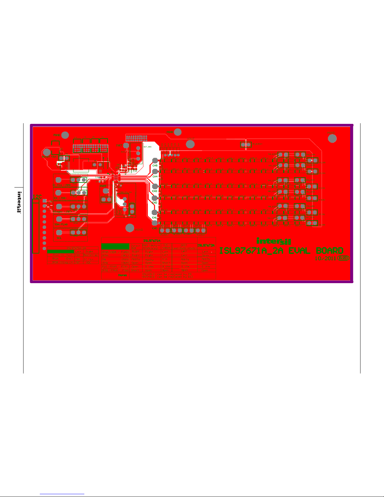
FIGURE 4. TOP VIEW OF ISL97671A/ISL97672A EVALUATION BOARD
Page 5
Application Note 1634
5
AN1634.1
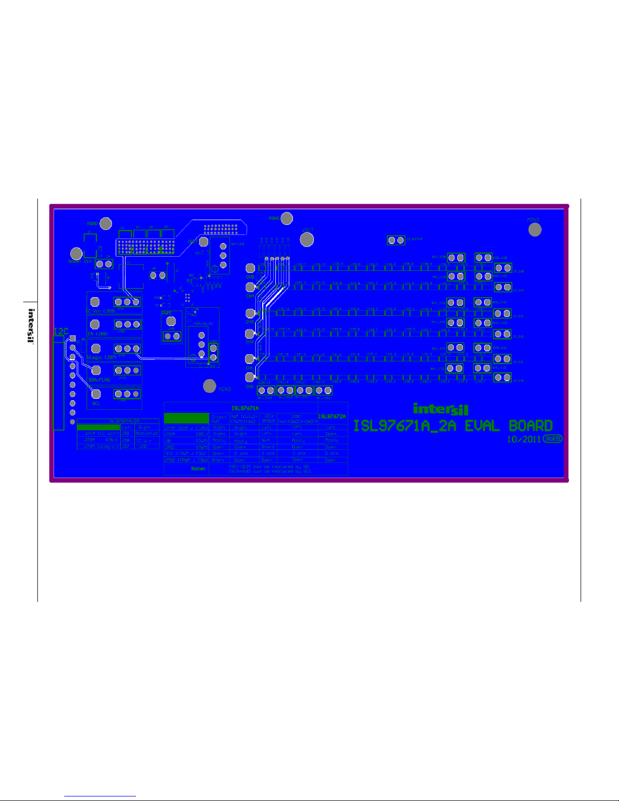
FIGURE 5. BOTTOM VIEW OF ISL97671A/ISL97672A EVALUATION BOARD
Page 6
Application Note 1634
6
AN1634.1
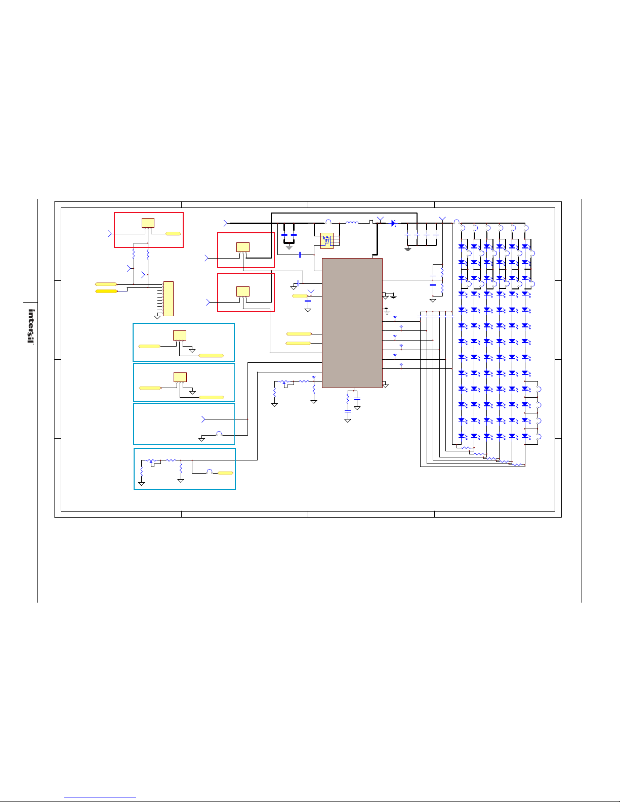
FIGURE 6. SCHEMATIC OF ISL97671A ISL97672A EVALUATION BOARD
A
B
C
D
D
C
B
A
Title
Size:
Date:
File:
Revision:
Sheet
B
Drawn By:
Error : intersil.bmp file not found.
Terry Nguyen
09/2011
C2
0.1uF/50V
C7
1uF/10V
L1
15uH(Coilcraft)
D1
PMEG6030
R2A
10K
R1
358K
C9
100pF/50V
C10
nc
C3
J98 (EN)
EN
J4 (SDA)
SDA / FLAG
J3 (SCL)
SCL
J1(Boost in)
Boost Vin
J9A
LX
R6
4.7k
R7
4.7k
J97 (I2C Vlogic)
Vlogic
C4C5C6
JP1
C1
10uF/50V
LED5_1
LED5_2
LED5_3
LED5_4LED5_5LED5_6LED5_7LED5_8LED5_9LED5_10LED5_11LED5_12LED5_13
LED4_1LED4_2
LED4_3
LED4_4
LED4_5LED4_6LED4_7LED4_8LED4_9LED4_10LED4_11LED4_12LED4_13
LED3_1LED3_2
LED3_3
LED3_4LED3_5
LED3_6
JP_CH5 JP_CH4 JP_CH3 JP_CH2
LED3_7
LED3_8LED3_9LED3_10LED3_11
LED3_12
LED3_13
LED2_1
JP_CH1
LED2_2
LED2_3
LED2_4LED2_5LED2_6
LED2_7
LED2_8
LED2_9
JP_CH0
LED1_3
LED1_4
LED1_5
LED1_6LED1_7
LED1_8LED1_9
LED1_10LED1_12LED1_13
LED0_1
LED0_2LED0_3
LED0_4
LED0_5
LED0_6
LED2_10LED2_11LED2_12LED2_13
LED1_1
LED1_11
LED0_7
LED1_2
LED0_8
LED0_9
LED0_10LED0_11LED0_12LED0_13
SH2_LED4 SH2_LED3
SH2_LED2
SH2_LED1 SH2_LED0SH2_LED5
C14
1nF
C13
1nF
C12
1nF
C11
1nF
C15
1nF
C16
1nF
CH4
CH5
C3 ~ C6 : 4.7uF/50V X7R
ceramic caps
C4~C6 are reserved pads
CH0
CH1
CH2
CH3
J10(Vout)
Vout
JP_OUTPUT
SDA
SCL
J9(VDC)
VDC
For 2 layers
board, connect
top layer PGND
and bottom laye
r
AGND at one
point such that
using the
thermal pad as a
single
SH_LED13
SH_LED12
SH_LED11
SH_LED10
FAULT
1
VIN
2
EN
3
VDC
4
PWM
5
SMBDAT or SDA / FLAG
6
SMBCLK or SCL / NC
7
FPWM / FSW
8
AGND
9
CH0
10
CH1
11
CH2
12
CH3
13
CH4
14
CH5
15
OVP
16
RSET
17
COMP
18
PGND
19
LX
20
PAD
C
U1
ISL97671A/72A
J81 (PWMI_direct)
PWMI
1
2
3
4
5
6
7
8
9
10
HDR1
INTERFACE
1
2
5
6
4
3
Q1
FDMA530PZ
12
WR
C18
nc
C19
0.1uF
J99( IC Vin)
IC Vin
IC
Vin=Bootstrap
IC Vin=
header
VDC
SCL_S
EN selection
IC VIN selection
SCL_IC
SDA_IC
SCL_IC
EN=IC Vin
(Right)
EN=J98 header
(Left)
SDA_IC
SDA_S
SCL_S
VDC
I2C / FLAG Vlogic selection
Vlogic=J97
header
Vlogic=VDC
(Right)
123
JP1A
123
JP2A
123
JP3A
123
JP5A
123
JP4A
JP91
JP92
VDC
ISET
R13
nc
R15
1M
R16
5K
R14
0
R9
nc
R11
750K
R12
2.21K
R10
0
C20
390pF
R2
10k
C8
3.3nF
ISL97671_2A EVAL SCHEMATIC
SH3-4
nc
SH2-3
nc
SH1-2
nc
SH5-6
nc
SH4-5
nc
SDA_S
SH1_LED4 SH1_LED3
SH1_LED2
SH1_LED1 SH1_LED0
SH1_LED5
Page 7
Application Note 1634
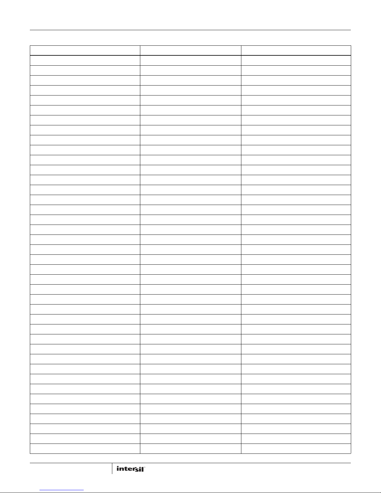
TABLE 1. BOM FOR ISL97671A/ISL97672A EVALUATION BOARD
PART TYPE DESIGNATOR FOOTPRINT
0 R14 402
0R10402
0.1uF C19 402
0.1µF/50V C2 402
1M R15 VRES
1nF C11 603
1nF C14 603
1nF C16 603
1nF C13 603
1nF C12 603
1nF C15 603
1µF/10V C7 402
2.21k R12 402
3.3nF C8 402
4.7k R6 603
4.7k R7 603
4.7µF/50V C5 1210
4.7µF/50V C6 1210
4.7µF/50V C3 1210
4.7µF/50V C4 1210
5k R16 402
10k R2A 402
10k R2 402
10µF/50V C1 1210
15µH (Coilcraft) L1 XAL6060-153MEB
100pF/50V C9 402
358K R1 402
390pF C20 402
750k R11 VRES
FDMA530PZ Q1 microFET2x2
INTERFACE HDR1 MOLEX22-05-3101
ISL97671A/72A U1 LPP20.3X4
LED-SMT ALL LEDs LW_Y87C
PMEG6030 D1 SOD-123W
nc SH4-5 402
nc C10 402
nc R13 402
nc C18 402
nc R9 402
nc SH3-4 402
7
AN1634.1
Page 8

Application Note 1634
TABLE 1. BOM FOR ISL97671A/ISL97672A EVALUATION BOARD
PART TYPE DESIGNATOR FOOTPRINT
nc SH5-6 402
nc SH1-2 402
nc SH2-3 402
(Continued)
Intersil Corporation reserves the right to make changes in circuit design, software and/or specifications at any time without notice. Accordingly, the reader is
cautioned to verify that the Application Note or Technical Brief is current before proceeding.
For information regarding Intersil Corporation and its products, see www.intersil.com
8
AN1634.1
 Loading...