

查询ISL21007CFB820Z供应商
®
ISL97653A
Data Sheet December 6, 2007
5-Channel Integrated LCD Supply
The ISL97653A represents a fully integrated supply IC for
LCD-TV applications. With an input operating range of 4V to
14V, both commonly used LCD-TV input supplies, 5V and
12V, are supported. An A
supply up to 20V is generated
VDD
by a high-performance PWM BOOST converter with an
integrated 4.4A FET. V
is generated using an integrated
ON
charge pump with on-chip diodes and can be modulated using
an on-chip V
slice control circuit. V
ON
is generated using
OFF
an integrated charge pump controller . Addi tional ly, the chip
allows for two logic supplies. A buck regulator with an
included 2.5A high side switch is used for the main logic
output and an internal LDO controller can be used to generate
a second logic LDO output.
To facilitate production test, an integrated HVS circuit is
included which can provide high voltage stress of the LCD
panel.
An on-board temperature sensor is also provided for system
thermal management control.
The ISL97653A is packaged in a 40 Ld 6mmx6mm QFN
package and is specified for operation over the -40°C to
+105°C temperature range.
Ordering Information
FN6367.0
Features
• 5V to 14V Input Supply
• Integrated 4.4A Boost Converter
• Integrated VON Charge Pump and VON Slice Circuit
• Integrated V
Charge Pump Output
OFF
• Integrated 2.5A Buck Converter
• LDO Controller for an Additional Logic Supply
• High Voltage Stress (HVS) Test Mode
• Thermal Shutdown
• 40 Ld QFN (6mmx6mm) Package
• Pb-Free (RoHS Compliant)
Applications
•LCD-TVs
• Industrial/Medical LCD Displays
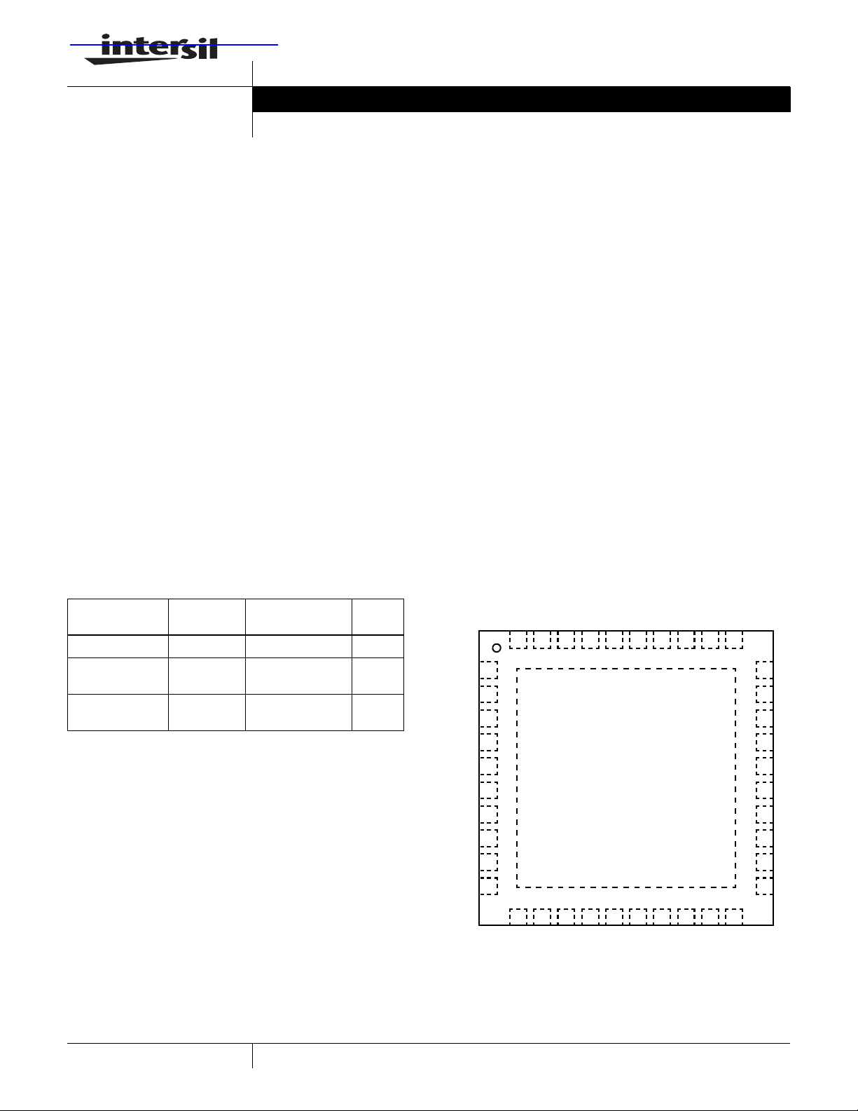
Pinout
ISL97653A
40 LD 6X6 QFN
TOP VIEW
PART NUMBER
(Note)
ISL97653AIRZ ISL97 653A 40 Ld 6 X6 QFN L40.6X6
ISL97653AIRZ-T* ISL97 653A 40 Ld 6 X 6 QFN
ISL97653AIRZ-TK* ISL97 653A 40 Ld 6 X 6 QFN
*Please refer to TB347 for details on reel specifications.
NOTE: These Intersil Pb-free plastic packaged products employ
special Pb-free material sets; molding compounds/die attach
materials and 100% matte tin plate PLUS ANNEAL - e3 termination
finish, which is RoHS compliant and compatible with both SnPb and
Pb-free soldering operations. Intersil Pb-free products are MSL
classified at Pb-free peak reflow temperatures that meet or exceed
the Pb-free requirements of IPC/JEDEC J STD-020.
PART
MARKING
PACKAGE
(Pb-Free)
Tape and Reel
Tape and Reel
PKG.
DWG. #
L40.6X6
L40.6X6
PVIN2
CB
LXL1
LXL2
PGND3
PGND4
CM2
FBL
VL
VREF
LDO-CTL
LDO-FB
PVIN1
AGND
PROT
LX2
LX1
40
39 38 37 36 35 34 33 32 31
1
2
3
4
5
6
7
8
9
10
11 12 13 14 15 16 17 18 19 20
FBN
SUPN
NOUT
C1P
PGND5
C2P
C1N
PGND2
C2N
PGND1
SUPP
TEMP
FBP
30
COMP
29
FBB
28
RSET
27
HVS
26
EN
CDEL
25
CTL
24
DRN
23
COM
22
21
POUT
1
CAUTION: These devices are sensitive to electrostatic discharge; follow proper IC Handling Procedures.
1-888-INTERSIL or 1-888-468-3774
| Intersil (and design) is a registered trademark of Intersil Americas Inc.
All other trademarks mentioned are the property of their respective owners.
Copyright Intersil Americas Inc. 2007. All Rights Reserved
ISL97653A
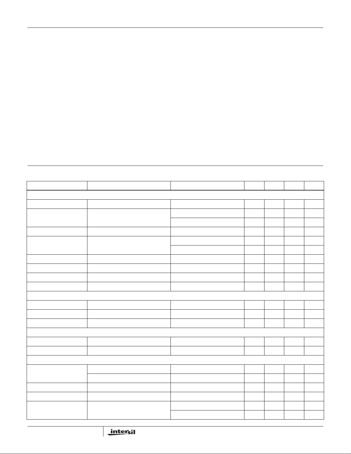
Absolute Maximum Ratings (T
Maximum Pin Voltages, all pins except below. . . . . . . . . . . . . . 6.5V
LX1, LX2, SUPP, SUPN, NOUT, PROT, C1N, C2N . . . . . . . . .24V
PVIN1, PVIN2, LXL1, LXL2 . . . . . . . . . . . . . . . . . . . . . . . . . 16.8V
EN, CTL . . . . . . . . . . . . . . . . . . . . . . . . . . . . . . . . . . . . . . . . 16.5V
= +25°C) Thermal Information
A
Operating Ambient Temperature Range . . . . . . . . -40°C to +105°C
Operating Junction Temperature . . . . . . . . . . . . . . -40°C to +150°C
Pb-free reflow profile . . . . . . . . . . . . . . . . . . . . . . . . . .see link below
http://www.intersil.com/pbfree/Pb-FreeReflow.asp
DRN, POUT, COM, C1P, C2P. . . . . . . . . . . . . . . . . . . . . . . . . .33V
CB . . . . . . . . . . . . . . . . . . . . . . . . . . . . . . . . . . . . . . . . . . . . . .21V
Recommended Operating Conditions
Input Voltage Range, VIN . . . . . . . . . . . . . . . . . . . . . . . . 4V to 14V
Input Capacitance, C
Boost Output Voltage Range, A
Output Capacitance, C
Boost Inductor, L1 . . . . . . . . . . . . . . . . . . . . . . . . . . . . . 3.3µH-10µH
V
Output Range, VON . . . . . . . . . . . . . . . . . . . . . . +15V to +30V
ON
V
Output Range, V
OFF
Logic Output Voltage Range, V
Buck Inductor, L2. . . . . . . . . . . . . . . . . . . . . . . . . . . . 3.3µH to 10µH
CAUTION: Do not operate at or near the maximum ratings listed for extended periods of time. Exposure to such conditions may adversely impact product reliability and
result in failures not covered by warranty.
Electrical Specifications V
PARAMETER DESCRIPTION CONDITIONS MIN TYP MAX UNIT
SUPPLY PINS
V
IN
I
S
F
SW
V
REF
VLOR Undervoltage Lockout Threshold V
VLOF Undervoltage Lockout Threshold V
LOGIC SIGNALS HVS, EN, CTL
Logic Input High 2.0 V
Logic Input Low 0.4 V
Pull-down Resistance 130 174 215 kΩ
HVS, RSET
RSET RSET Pull-down Resistance HVS = HIGH 200 Ω
I
RSET
A
BOOST
VDD
DLIM Min Duty Cycle 8.5 12 %
V
BOOST
EFF
BOOST
V
FB
. . . . . . . . . . . . . . . . . . . . . . . . . . . . .2x10µF
IN
. . . . . . . . . . . . . . . . . . . . . . . . . .3x22µF
OUT
. . . . . . . . . . . . . . . . . . . . . . .-15V to -5V
OFF
. . . . . . . . . . . . . . . . . . . . +20V
VDD
. . . . . . . . . . . .+1.5V to +3.3V
LOGIC
= 12V , V
IN
unless otherwise stated.
BOOST
= V
SUPN
Supply Voltage 4 14 V
Quiescent Current Enabled, no switching 4 5 mA
Switching Frequency 580 680 780 kHz
Reference Voltage TA = +25°C 1.190 1.215 1.240 V
Thermal Shutdown Temperature rising 150 °C
Thermal Shutdown Hysteresis 20 °C
RSET Leakage Current HVS = LOW, V
Max Duty Cycle 90 %
Boost Output Range 20 V
Boost Efficiency VIN = 12V, V
Boost Feedback Voltage TA = +25°C 1.203 1.215 1.227 V
= V
= 15V , VON = 25V , V
SUPP
= -8V , over temperature from -40°C to +105°C,
OFF
Disabled 2.7 3.5 mA
1.187 1.215 1.243 V
rising 3.4 3.55 3.7 V
L
falling 2.9 3.0 3.2 V
L
= 1.2V 0.4 µA
RSET
= 15V 90+ %
BOOST
1.198 1.215 1.232 V
2
FN6367.0
December 6, 2007
ISL97653A
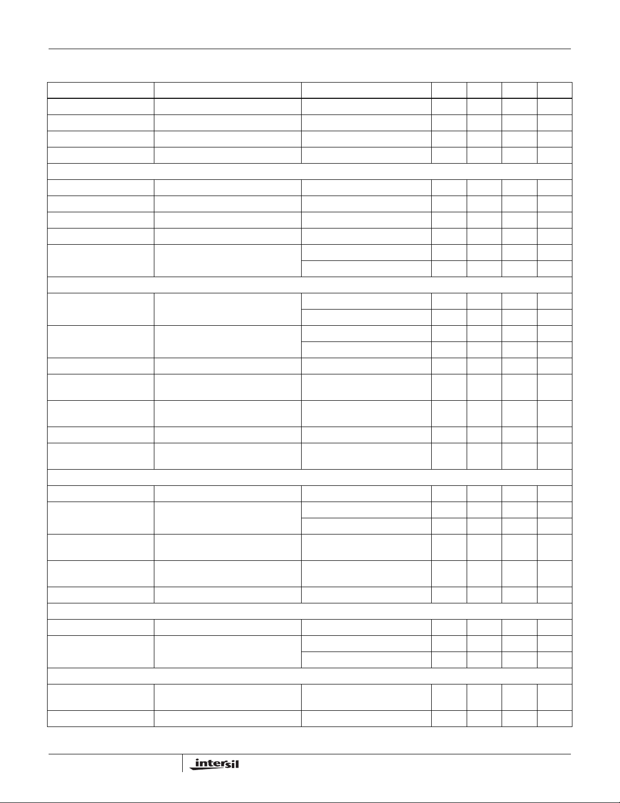
Electrical Specifications V
= 12V , V
IN
unless otherwise stated. (Continued)
BOOST
= V
SUPN
= V
SUPP
= 15V , VON = 25V , V
= -8V , over temperature from -40°C to +105°C,
OFF
PARAMETER DESCRIPTION CONDITIONS MIN TYP MAX UNIT
I
BOOST
R
DSON-BOOST
ΔV
BOOST
ΔV
BOOST
/ΔV
/ΔI
IN
OUT
Boost FET Current Limit 3.7 4.4 4.95 A
Switch On Resistance 93 200 mΩ
Line Regulation - Boost 0.08 0.15 %
Load Regulation - Boost Load 100mA to 200mA 0.004 1 %
LOGIC BUCK
EFF
BUCK
I
BUCK
R
DSON-BUCK
ΔV
/ΔI
LDO
V
FL
OUT
Buck Efficiency VIN = 5V, V
= 3.3V 90+ %
LOGIC
Buck FET Current Limit 1.9 4.0 A
Switch On Resistance 150 210 mΩ
Load Regulation - Buck Load 100mA to 500mA 0.5 1 %
Feedback Voltage TA = +25°C 1.195 1.215 1.235 V
1.189 1.215 1.241 V
V
CHARGE PUMP
ON
ILoad_PCP_min External Load Driving Capability V
= 24V (2X Charge Pump) 40 mA
ON
VON = 28V (3X Charge Pump) 40 mA
V
FBP
Feedback Voltage, ION = 1mA TA = +25°C 1.195 1.215 1.235 V
1.189 1.215 1.241 V
R
(VSUP_SW) ON Resistance of V
ON
R
(C1/2-)H High-Side Driver ON Resistance at
ON
(C1/2-)L Low-Side Driver ON Resistance at
R
ON
V
Load Reg VON Output Load Regulation ION = 10mA to 40mA +1 %
ON
C1- and C2-
C1- and C2-
V(diode) Internal Schottky Diode Forward Voltage
Input Switch I(switch) = +40mA 10 17 Ω
SUP
I(C1/2-) = +40mA 30 Ω
I(C1/2-) = -40mA 4 10 Ω
I(diode) = +40mA 700 800 mV
Drop
V
CHARGE PUMP
OFF
ILoad_NCP_min External Load Driving Capability SUPN>13.5V VOFF=-8V 100 120 mA
V
FBN
Feedback Voltage, I
= 10mA TA = +25°C 0.173 0.203 0.233 V
OFF
0.171 0.203 0.235 V
R
(NOUT)H High-Side Driver ON Resistance at
ON
R
(NOUT)L Low-Side Driver ON Resistance at
ON
NOUT
I(NOUT) = +60mA 10 Ω
I(NOUT) = -60mA 5 Ω
NOUT
V
Load Reg V
OFF
Output Load Reg I
OFF
= 10mA to 100mA, TA = +25°C 2.4 %
OFF
LDO Controller
I
DRVP
LDO-FB Feedback Voltage w/transistor load 1mA T
Sink Current V
= 1.1V, V
FBP
= +25°C 1.191 1.215 1.239 V
A
LDO_CTL
= 10V 12 15 mA
1.189 1.215 1.241 V
FAULT DETECTION THRESHOLDS
T_off Thermal Shut-Down (latched and reset
Temperature rising 150 °C
by power cycle or EN cycle)
Vth_A
(FBB) A
VDD
Boost Short Detection V(FBB) falling less than 0.9 V
VDD
3
FN6367.0
December 6, 2007
ISL97653A
Electrical Specifications V
= 12V , V
IN
unless otherwise stated. (Continued)
BOOST
= V
SUPN
= V
SUPP
= 15V , VON = 25V , V
= -8V , over temperature from -40°C to +105°C,
OFF
PARAMETER DESCRIPTION CONDITIONS MIN TYP MAX UNIT
Vth_POUT (FBP) P
Vth_NOUT (FBN) N
V
Slice POSITIVE SUPPLY = V(POUT)
ON
I(POUT)_slice V
Charge Pump Short Detection V(FBP) falling less than 0.9 V
OUT
Charge Pump Short Detection V(FBN) rising more than 0.4 V
OUT
Slice Current from POUT Supply CTL = VDD, sequence complete 400 500 µA
ON
CTL = AGND, sequence complete 150 200 µA
R
(POUT-COM) ON Resistance between POUT-COM CTL = VDD, sequence complete 5 10 Ω
ON
R
(DRN-COM) ON Resistance between DRN-COM CTL = AGND, sequence complete 30 60 Ω
ON
RON_COM ON Resistance between DRN-COM and
200 260 400 Ω
PGND
PROT
I
PROT_ON
I
PROT_OFF
PROT Pull-Down Current or Resistance
when Enabled by the Start-U
PROT Pull-Up Current when Disabled V
V
> 0.9V 38 50 60 µA
PROT
V
< 0.9V 500 760 1000 Ω
PROT
< 20V 2 3 4 mA
PROT
4
FN6367.0
December 6, 2007
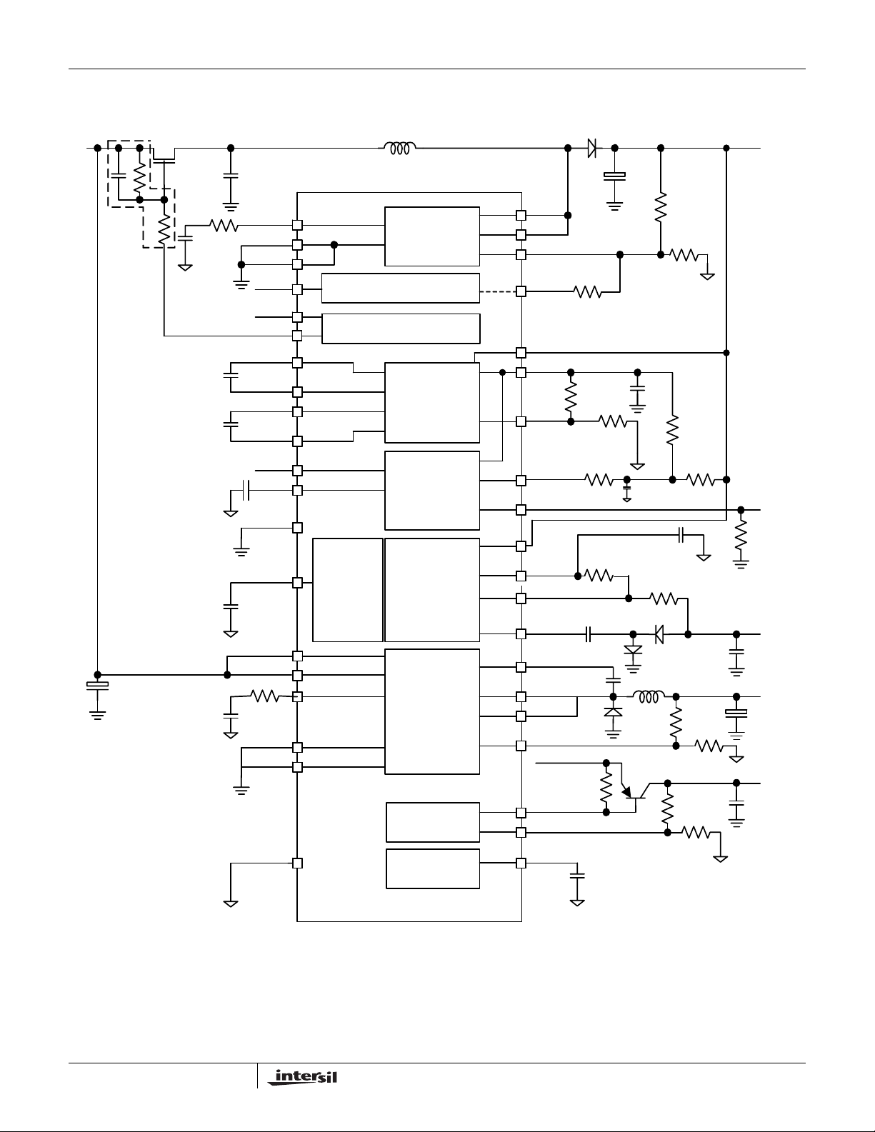
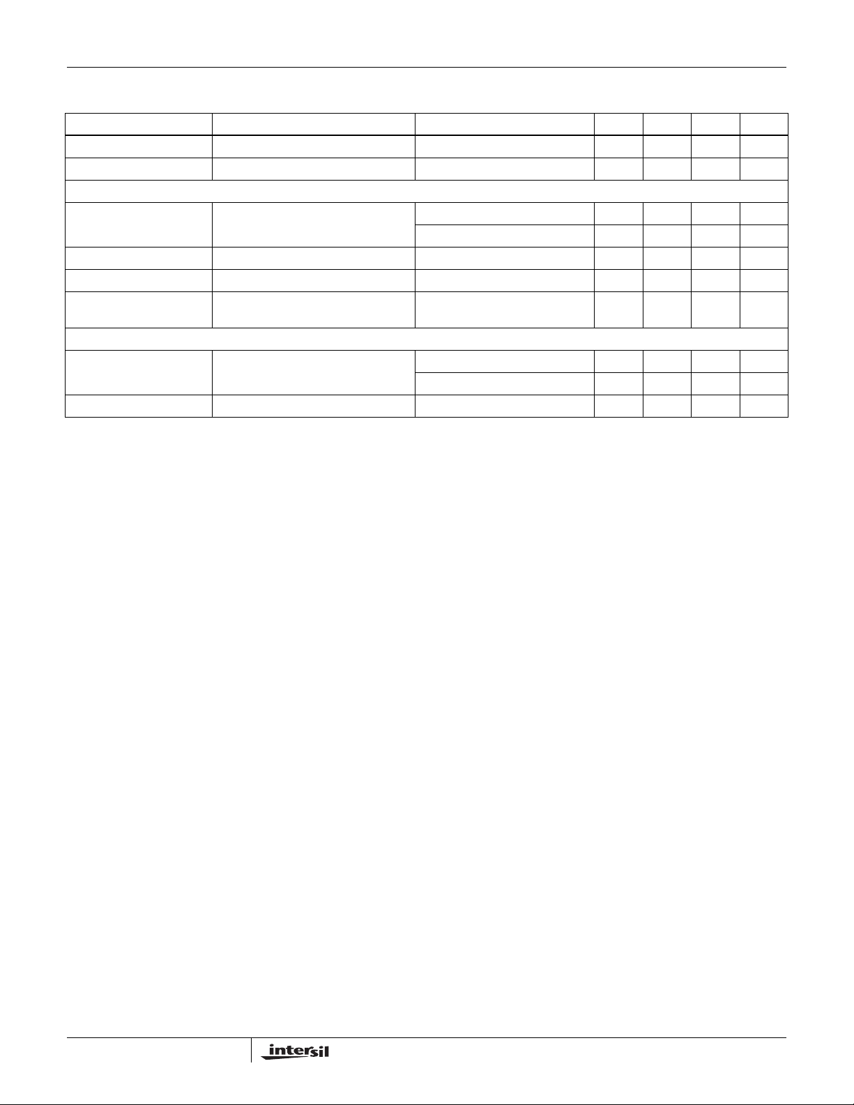
Typical Application Diagrams
ISL97653A
V
IN
C30
Optional
R21 75k
C0
10µF
M0
R22 75k
C2
4.7nF
220nF
220nF
C4
C5
C6
0.22µF
C7
4.7µF
C8
4.7nF
R2
0
C1
2.2µF
COMP
PGND1
PGND2
HVS
PROT
C1P
C1N
C2P
C2N
CTL
CDEL
PGND5
PVIN1
PVIN2
CM2
R20 10k
PGND3
PGND4
AGND
EN
VL
L
L1
6.8µH
30
32
33
27
HVS
26
SEQUENCING/FAULT CONTROL
36
15
16
17
18
24
25
VON SLICE
14
9
INTERNAL
REGULATOR
38
1
7
5
6
LDO CONTROLLER
37
TEMP SENSOR
BOOST
VON CP
V
CP
OFF
BUCK
D1
A
VDD
C3
22µF
x3
LX1
34
LX2
35
FBB
29
RSET
28
R3
55k
R4
5k
R5 20k
19
SUPP
21
POUT
V
R6
983k
20
FBP
470nF
R7, 50k
DRN
23
COM
22
12
SUPN
10
VREF
FBN
11
NOUT
13
R10
15
R11 40k
C22 0.1µF
C11
220nF
CB
2
C13
LXL1
3
LXL2
4
FBL
8
V
1µF
D4
LOGIC
D3
L
L2
6.8µH
R17
LDO-CTL
40
39
LDO-FB
TEMP
31
Q1
C9
R13
2k
R8
1k
C19
220nF
D2
R15
5.4k
R16
5k
ON
R9
1k
R12
328k
470nF
R14
1.2k
C12
C14
20µF
V
V
V
LOGIC
LOGIC2
R17
100k
OFF
C15
4.7µF
C16
10nF
5
FN6367.0
December 6, 2007
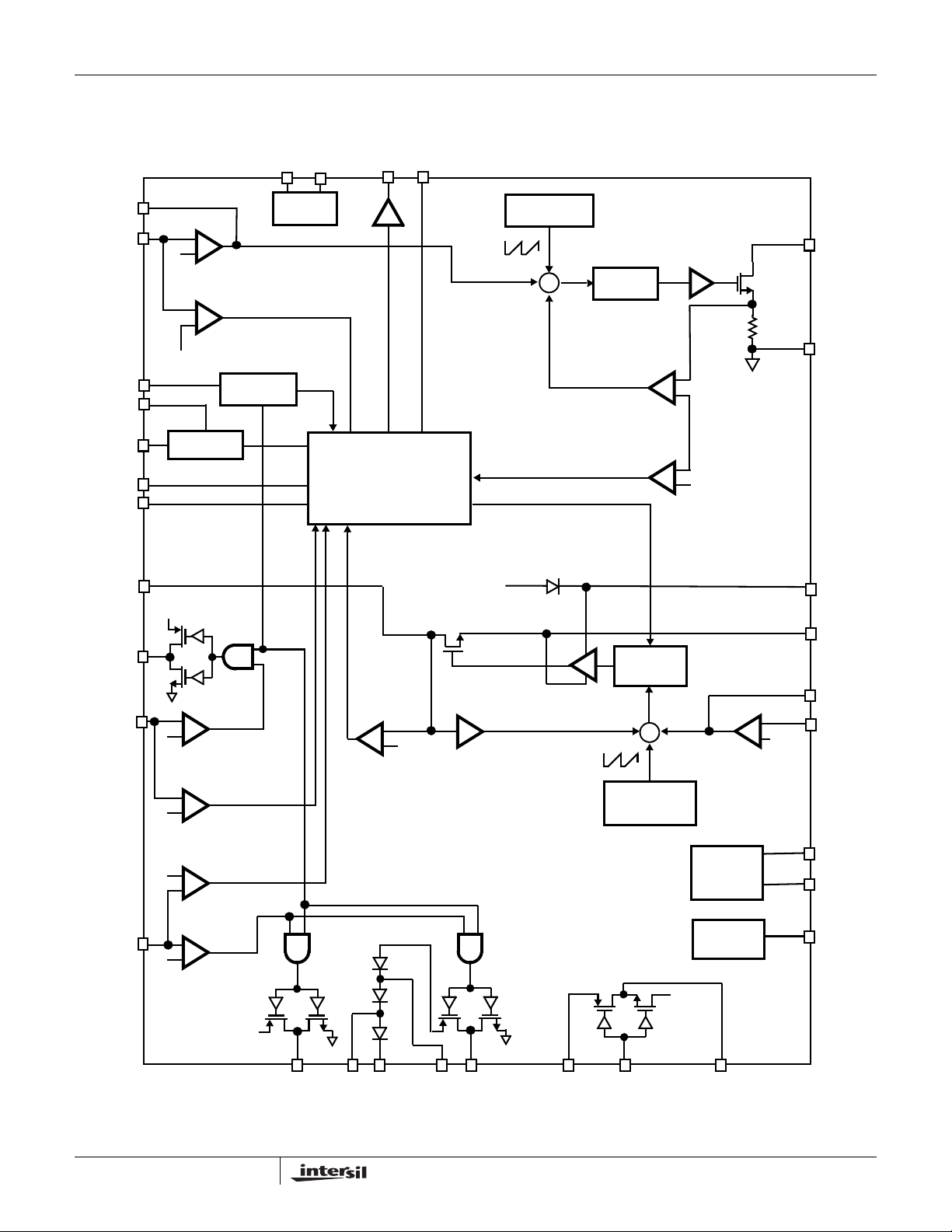
Typical Application Diagrams (Continued)
ISL97653A
FREQ
P
VIN1,2
CDEL
P
VIN1,2
N
CM1
FBB
VL
EN
OUT
FBN
GM AMPLIFIER
+
V
REF
UVLO COMPARATOR
+
0.75 V
REF
OSCILLATOR
REGULATOR
SUPN
+
0.2V
UVLO COMPARATOR
+
0.4V
RSET HVS PROT
HVS
LOGIC
680kHz
REFERENCE BIAS
SEQUENCE CONTROLLER
CURRENT
COMPARATOR
V
REF
AND
LIMIT
-
+
CURRENT LIMIT
THRESHOLD
SAWTOOTH
GENERATOR
SLOPE
COMPENSATION
Ε
VL
CURRENT AMPLIFIER
CONTROL
BUFFER
LOGIC
CURRENT
AMPLIFIER
CURRENT LIMIT
COMPARATOR
CONTROL
LOGIC
Ε
SLOPE
COMPENSATION
SAWTOOTH
GENERATOR
BUFFER
CURRENT LIMIT
THRESHOLD
GM AMPLIFIER
LX1
LX2
R
SENSE
-
+
V
REF
PGND1
PGND2
CB
LXL1
LXL2
CM2
FBL
FBP
0.75 V
V
REF
REF
+
+
SUPP
C1- C1+ C2+ C2-P
6
SUPP
OUT
DRN
LDO
CONTROL
LOGIC2
TEMP
SENSOR
P
OUT
CTL COM
LDO-CTL
LDO-FB
TEMP
FN6367.0
December 6, 2007

Typical Performance Curves
100
ISL97653A
0.5
90
VIN = 5V
80
EFFICIENCY (%)
70
0 500 1000 1500
VIN = 8V
(mA)
I
O
VIN = 12V
FIGURE 1. BOOST EFFICIENCY FIGURE 2. BOOST LOAD REGULATION
0.08
0.06
0.04
0.02
0.00
LINE REGULATION (%)
-0.02
-0.04
5 6 7 8 9 1011 121314
IO = 100mA
IO = 400mA
(V)
V
IN
FIGURE 3. BOOST LINE REGULATION FIGURE 4. BUCK EFFICIENCY
I
VIN = 8V
I
VIN = 8V
(mA)
O
(mA)
O
VIN = 12V
VIN = 12V
0.4
0.3
VIN = 5V
0.2
0.1
LOAD REGULATION (%)
0.0
0 500 1000 1500
100
90
80
70
EFFICIENCY (%)
60
50
0 500 1000 1500 2000
VIN = 5V
0.3
0.2
0.1
0.0
-0.1
-0.2
LOAD REGULATION (%)
-0.3
0 500 1000 1500 2000
VIN = 5V
VIN = 8V
I
O
VIN = 12V
(mA)
FIGURE 5. BUCK LOAD REGULATION FIGURE 6. BUCK LINE REGULATION
7
0.10
0.08
0.06
0.04
0.02
LINE REGULATION (%)
0.00
5678 9
IO = 100mA
V
IO = 400mA
10 11 12 13 14
(V)
IN
December 6, 2007
FN6367.0
Typical Performance Curves (Continued)
0
I
ON
VON = 25V
(mA)
-1
-2
-3
-4
LOAD REGULATION (%)
-5
0 102030405060
FIGURE 7. VON LOAD REGULATION FIGURE 8. VOFF LOAD REGULATION
ISL97653A
1.2
1.0
0.8
0.6
0.4
0.2
0.0
LOAD REGULATION (%)
-0.2
0 102030405060
VON = 25V
(mA)
I
ON
0.0
-0.2
-0.4
-0.6
-0.8
-1.0
-1.2
LOAD REGULATION (%)
-1.4
0 10 20 30 40 50 60 70 80 90 100 110 120 130 140 150
V
LOGIC
I
LDO
= 2.3V
(mA)
FIGURE 9. LOGIC LDO LOAD REGULATION
CH1 = A
CH2 = I
VDD (VBOOST
(BOOST) (100mA/DIV)
O
) (100mV/DIV)
CH1 = A
CH2 = I
VDD (VBOOST
(BOOST)(200mA/DIV)
O
)(500mV/DIV)
1ms/DIV
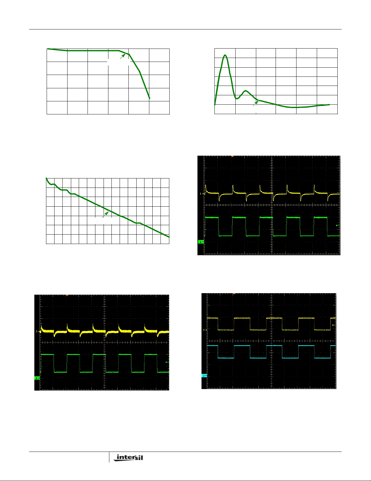
FIGURE 10. BOOST TRANSIENT RESPONSE
CH1 = VCTL (5V/DIV)
CH2 = COM (10V/DIV)
1ms/DIV
40µs/DIV
FIGURE 11. BUCK TRANSIENT RESPONSE FIGURE 12. VON SLICE OPERATION
8
FN6367.0
December 6, 2007

ISL97653A
Typical Performance Curves (Continued)
Ch1 = LXL (400ns/DIV)
Ch2 = ILXL (400ns/DIV)
FIGURE 13. BOOST CURRENT LIMIT FIGURE 14. BUCK CURRENT LIMIT
Pin Descriptions
PIN NUMBER PIN NAME DESCRIPTION
1 PVIN2 Logic buck supply voltage. This is also the analog supply from which the VL is generated. Needs at
least 1µF bypassing.
2 CB Logic buck boot strap pin. Generate the gate drive voltage for the N-Channel MOSFET by connecting
a 1µF cap to the switching node LXL1,2.
3, 4 LXL1, 2 Logic buck switching node. Source of the high side internal power N-Channel MOSFET for the Buck.
5, 6 PGND3,4 Logic buck ground pin.
7 CM2 Buck compensation pin. An RC network is recommended. Increase R for better transient response at
the expense of stability.
8 FBL Logic buck feedback pin. High impedance input to regulate at 1.215V.
9 VL 5.25V internal regulator output. Bypass with a 4.7µF cap. Ref voltage is generated from VL.
10 VREF Reference voltage output. Bypass with a low valued cap for transients - recommend 220nF. Should not
11 FBN Negative charge pump feedback pin. High impedance input to regulate to 0.203V.
12 SUPN Negative charge pump supply voltage. Can be the same as or different from A
13 NOUT Negative charge pump driver output.
14 PGND5 Charge pump ground pin.
15 C1P Charge pump capacitor 1, positive connection.
16 C1N Charge pump capacitor 1, negative connection.
17 C2P Charge pump capacitor 2, positive connection.
18 C2N Charge pump capacitor 2, negative connection.
19 SUPP Positive charge pump supply. Can be the same as or different from A
20 FBP Positive charge pump feedback pin. High impedance input to regulate at 1.215V
21 POUT V
22 COM High voltage switch control output. V
23 DRN Lower reference voltage for V
24 CTL Input control pin for V
be greater than 5 times CDEL cap to ensure correct start-up sequence.
charge pump output.
ON
slice output.
ON
slice output. Usually connected to A
ON
slice output.
ON
Ch1 = LXL (400ns/DIV)
Ch2 = ILXL (400ns/DIV)
VDD.
.
VDD
VDD.
9
FN6367.0
December 6, 2007

ISL97653A
Pin Descriptions (Continued)
PIN NUMBER PIN NAME DESCRIPTION
25 CDEL V
26 EN Chip enable (active high). Can be driven to VIN levels.
27 HVS High-voltage stress input select pin. High selects high voltage mode.
28 RSET Voltage set pin for HVS test. RSET connects to ground in the high voltage mode - RSET high.
29 FBB A
30 COMP Boost compensation network pin. An RC network is recommended. Increase R for better transient
31 TEMP Temperature sensor output voltage. An analog voltage from 0V to 3V for temperatures of -40°C to
32, 33 PGND1, 2 Boost ground pins.
34, 35 LX1, 2 Boost switch output. Drain of the internal power NMOS for the Boost.
36 PROT Gate driver of the Input protection switch. Goes low when EN is high. Can be used to modulate the
37 AGND Analog ground. Separate from PGND’s and star under the chip.
38 PVIN1 Logic buck supply voltage.This is also the analog supply from which the VL is generated. Needs at least
39 LDO-FB LDO controller feedback. High impedance input to regulate at 1.215V.
40 LDO-CTL LDO control pin. Gate drive for the external PNP BJT.
slice control delay input. Minimum 47nF . Recommend 220nF but is only limited by leakage in the
ON
cap reaching µA levels.
boost feedback pin. High impedance input to regulate at 1.215V.
VDD
response at the expense of stability. An R = 0Ω is recommended for 4.4A Boost requirements.
+150°C.
passive input inrush current as shown by R
1µF bypassing.
, and C30 in the typical application diagram.
21,R22
10
FN6367.0
December 6, 2007
Δ
ISL97653A
Application Information
A
Boost Converter
VDD
The A
boost FET. The regulator uses a current mode PI control
scheme which provides good line regulation and good
transient response. It can operate in both discontinuous
conduction mode (DCM) at light loads and continuous mode
(CCM). In continuous current mode, current flows
continuously in the inductor during the entire switching cycle
in steady state operation. The voltage conversion ratio in
continuous current mode is given by Equation 1:
V
boost
------------------
V
where D is the duty cycle of the switching MOSFET.
The boost soft-start function is digitally controlled within a
fixed 10ms time frame during which the current limit is
increased in eight linear steps.
The boost converter uses a summing amplifier architecture
for voltage feedback, current feedback, and slope
compensation. A comparator looks at the peak inductor
current cycle by cycle and terminates the PWM cycle if the
current limit is triggered. Since this comparison is cycle
based, the PWM output will be released after the peak
current goes below the current limit threshold.
An external resistor divider is required to divide the output
voltage down to the nominal reference voltage. Current
drawn by the resistor network should be limited to maintain
the overall converter efficiency. The maximum value of the
resistor network is limited by the feedback input bias current
and the potential for noise being coupled into the feedback
pin. A resistor network in the order of 60kΩ is recommended.
The boost converter output voltage is determined by
Equation 2:
A
VDD
where R
stated, component variables referred to in equations refer to
the Typical Application Diagram.
The current through the MOSFET is limited to 4.4A peak.
This restricts the maximum output current (average) based
on Equation 3:
I
OMAXILMT
Where ΔIL is peak to peak inductor ripple current, and is set
by Equation 4. f
I
boost converter features a fully integrated 4.4A
VDD
1
-------------
=
1D–
IN
R3R4+
---------------------
3
V
IN
---------
L
L
×=
V
R
FBB
4
and R4 are in the “” on page 5. Unless otherwise
ΔI
V
L
--------
IN
---------
×=
2
V
O
⎛⎞
–
⎝⎠
is the switching frequency (680kHz).
s
D
---- -
×=
f
S
(EQ. 1)
(EQ. 2)
(EQ. 3)
(EQ. 4)
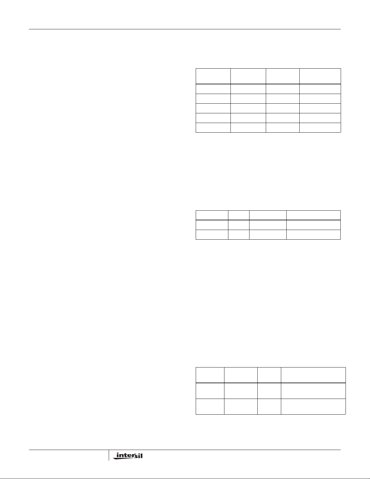
Table 1 gives typical values (worst case margins are
considered 10%, 3%, 20%, 10% and 15% on V
F
and I
SW
TABLE 1. MAXIMUM OUTPUT CURRENT CALCULATION
V
IN
(V)
5 9 6.8 2215
5 12 6.8 1673
5 15 6.8 1344
12 15 6.8 3254
12 18 6.8 2670
OMAX
):
V
(V)
O
L
(µH)
, VO, L,
IN
I
OMAX
(mA)
Boost Converter Input Capacitor
An input capacitor is used to suppress the voltage ripple
injected into the boost converter. A ceramic capacitor with
capacitance larger than 10µF is recommended. The voltage
rating of input capacitor should be larger than the maximum
input voltage. Some capacitors are recommended in Table 2
for input capacitor.
TABLE 2. BOOST CONVERTER INPUT CAP ACITOR
RECOMMENDATION
CAPACITOR SIZE VENDOR PART NUMBER
10µF/25V 1210 TDK C3225X7R1E106M
10µF/25V 1210 Murata GRM32DR61E106K
Boost Inductor
The boost inductor is a critical part which influences the
output voltage ripple, transient response, and efficiency.
Values of 3.3µH to 10µH are recommended to match the
internal slope compensation as well as to maintain a good
transient response performance. The inductor must be able
to handle the average and peak currents expressed in
Equations 5 and 6:
I
O
I
LAVG
I
LPKILAVG
Some inductors are recommended in Table 3.
INDUCTOR
5.1A
-------------
=
1D–
ΔI
L
--------
+=
2
TABLE 3. BOOST INDUCTOR RECOMMENDATION
DIMENSIONS
(mm) VENDOR PART NUMBER
10µH/
PEAK
5.9µH/
6A
PEAK
13x13x4.5 TDK RLF12545T-100M5R1
12.9X12.9X4 Sumida CDEP12D38NP-5R9MB-120
(EQ. 5)
(EQ. 6)
11
FN6367.0
December 6, 2007

ISL97653A
Rectifier Diode (Boost Converter)
A high-speed diode is necessary due to the high switching
frequency. Schottky diodes are recommended because of
their fast recovery time and low forward voltage. The reverse
voltage rating of this diode should be higher than the
maximum output voltage. The rectifier diode must meet the
output current and peak inductor current requirements. The
following table lists two recommendations for boost
converter diode.
TABLE 4. BOOST CONVERTER RECTIFIER DIODE
DIODE
FYD0504SA 50V/2A DPAK Fairchild
30WQ04FN 40V/3.5A DPAK International
RECOMMENDATION
V
R/IAVG
RATING PACKAGE VENDOR
Semiconductor
Rectifier
Output Capacitor
Integrating output capacitors supply the load directly and
reduce the ripple voltage at the output. Output ripple voltage
consists of two components: the voltage drop due to the
inductor ripple current flowing through the ESR of output
capacitor, and the charging and discharging of the output
capacitor.
V
RIPPLEILPK
ESR
V
–
OVIN
----------------------- -
V
O
I
O
----------------
C
OUT
1
----
××+×=
f
s
(EQ. 7)
Stability can be examined by repeatedly changing the load
between 100mA and a max level that is likely to be used in
the system being used. The A
voltage should be
VDD
examined with an oscilloscope set to AC 100mV/DIV and the
amount of ringing observed when the load current changes.
Reduce excessive ringing by reducing the value of the
resistor in series with the CM1 pin capacitor.
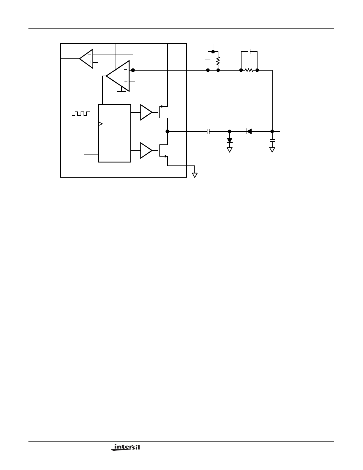
Cascaded MOSFET Application
A 20V N-Channel MOSFET is integrated in the boost
regulator. For applications requiring output voltages greater
than 20V, an external cascaded MOSFET is needed as
shown in Figure 15. The voltage rating of the external
MOSFET should be greater than A
VIN
LX1, LX2
INTERSIL
ISL97653A
FIGURE 15. CASCADED MOSFET TOPOLOGY FOR HIGH
OUTPUT VOLTAGE APPLICATIONS
VDD
FBB
.
A
VDD
For low ESR ceramic capacitors, the output ripple is
dominated by the charging and discharging of the output
capacitor. The voltage rating of the output capacitor should
be greater than the maximum output voltage.
Note: Capacitors have a voltage coefficient that makes their
effective capacitance drop as the voltage across them
increases. C
in Equation 7 assumes the effective value
OUT
of the capacitor at a particular voltage and not the
manufacturer's stated value, measured at zero volts.
Table 5 shows some selections of output capacitors.
TABLE 5. BOOST OUTPUT CAPACITOR RECOMMENDATION
CAPACITOR SIZE VENDOR PART NUMBER
10µF/25V 1210 TDK C3225X7R1E106M
10µF/25V 1210 Murata GRM32DR61E106K
PI Loop Compensation (Boost Converter)
The boost converter of ISL97653A can be compensated by
a RC network connected from COMP pin to ground.
C
= 4.7nF and R2 = 0Ω to 10Ω. A RC network is used in the
2
demo board. A higher capacitor value can be used to
increase system stability.
V
Protection
IN
A series external P-FET can be used to prevent passive
power-up inrush current from the Boost output caps charging
to V
IN
- V
SCHOTTKY
via the boost inductor and Schottky
diode. This FET also adds protection in the event of a short
circuit on A
The gate of the PFET (shown as M0 in the “”
VDD.
on page 5) is controlled by PROT. When EN is low, PROT is
pulled internally to PVIN1, thus M0 is switched off. When EN
goes high, PROT is pulled down slowly via a 50µA current
source, switching M0 on.
If the device is powered up with EN tied to high, M0 will
remain switched off until the voltage on VL exceeds the
VLOR threshold. Once the voltage on PROT falls below 0.6V
and the step-up regulator is within 90% of its target voltage,
PROT is pulled down to ground via a 1.3kΩ impedance. If
A
falls 10% below regulation, the drive to PROT reverts
VDD
to a 50µA current source. If a timed fault is detected, M0 is
actively switched off.
Several additional external components can optionally be
used to fine-tune the function of pin PROT (shown in the
dashed box near M0 in application diagram). PROT ramp
rate can be controlled by adding a capacitor C30 between
gate and source of M0. M0 gate voltage can be limited
during soft-start by adding a resistor (~75kΩ) between gate
12
FN6367.0
December 6, 2007

ISL97653A
and source of M0. In addition, a resistor can be connected
between PROT and the gate of M0, in order to limit the
maximum V
of M0 at all times.
GS
Buck Converter
The buck converter is a step down converter supplying
power to the logic circuit of the LCD system. The ISL97653A
integrates a high voltage N-channel MOSFET to save cost
and reduce external component count. In the continuous
current mode, the relationship between input voltage and
output voltage as expressed in Equation 8:
V
LOGIC
--------------------- -
V
IN
D=
(EQ. 8)
Where D is the duty cycle of the switching MOSFET.
Because D is always less than 1, the output voltage of a
buck converter is lower than input voltage.
The peak current limit of buck converter is set to 2.5A, which
restricts the maximum output current (average) based on
Equation 9:
2.5A ΔI
I
OMAX
Where ΔI
–=
P-P
is the ripple current in the buck inductor as
P-P
(EQ. 9)
shown in Equation 10:
V
LOGIC
--------------------- -
ΔI
pp
Lfs⋅
Where L is the buck inductor, f
1D–()⋅=
is the switching frequency
s
(EQ. 10)
(680kHz).
Feedback Resistors
The buck converter output voltage is determined by
Equation 11:
R14R13+
V
LOGIC
-------------------------- -
×=
V
R
14
FBL
(EQ. 11)
Where I
is the output current of the buck converter. Table 6
o
shows some recommendations for input capacitor.
TABLE 6. INPUT CAPACITOR (BUCK) RECOMMENDATION
CAPACITOR SIZE VENDOR PART NUMBER
10µF/16V 1206 TDK C3216X7R1C106M
10µF/10V 0805 Murata GRM21BR61A106K
22µF/16V 1210 Murata C3225X7R1C226M
Buck Inductor
A 3.3µH to 10µH inductor range is recommended for the
buck converter. Besides the inductance, the DC resistance
and the saturation current are also factors that need to be
considered when choosing a buck inductor. Low DC
resistance can help maintain high efficiency. Saturation
current rating should be higher than 2A. Here are some
recommendations for buck inductor.
TABLE 7. BUCK INDUCTOR RECOMMENDATION
DIMENSIONS
INDUCTOR
4.7µH/
2.7A
PEAK
6.8µH/
3A
PEAK
(mm) VENDOR PART NUMBER
5.7x5.0x4.7 Murata LQH55DN4R7M01K
7.3x6.8x3.2 TDK RLF7030T-6R8M2R8
Rectifier Diode (Buck Converter)
A Schottky diode is recommended for fast recovery and low
forward voltage. The reverse voltage rating should be higher
than the maximum input voltage. The peak current rating is
2.5A, and the average current is given by Equation 13:
I
Where I
following table shows some diode recommended.
avg
1D–()*I
=
o
is the output current of buck converter. The
o
(EQ. 13)
Where R
and R
13
are the feedback resistors in the buck
14
converter loop to set the output voltage Current drawn by
the resistor network should be limited to maintain the overall
converter efficiency. The maximum value of the resistor
network is limited by the feedback input bias current and the
potential for noise being coupled into the feedback pin. A
resistor network in the order of 1kΩ is recommended.
Buck Converter Input Capacitor
Input capacitance should support the maximum AC RMS
current which occurs at D = 0.5 and maximum output
current.
I
() D1D–()⋅ IO⋅=
acrmsCIN
13
(EQ. 12)
TABLE 8. BUCK RECTIFIER DIODE RECOMMENDATION
V
DIODE
PMEG2020EJ 20V/2A SOD323F Philips
SS22 20V/2A SMB Fairchild
R/IAVG
RATING PACKAGE VENDOR
Semiconductors
Semiconductor
December 6, 2007
FN6367.0
ISL97653A
Output Capacitor (Buck Converter)
Four 10µF or two 22µF ceramic capacitors are recommended
for this part. The overshoot and undershoot will be reduced
with more capacitance, but the recovery time wi ll be longer.
TABLE 9. BUCK OUTPUT CAPACITOR RECOMMENDATION
CAPACITOR SIZE VENDOR PART NUMBER
10µF/6.3V 0805 TDK C2012X5R0J106M
10µF/6.3V 0805 Murata GRM21BR60J106K
22µF/6.3V 1210 TDK C3216X5R0J226M
100µF/6.3V 1206 Murata GRM31CR60J107M
PI Loop Compensation (Buck Converter)
The buck converter of ISL97653A can be compensated by a
RC network connected from CM2 pin to ground. C
and R
= 10k RC network is used in the demo board. A
20
= 4.7nF
8
larger value resistor can lower the transient overshoot,
however, at the expense of stability of the loop.
The stability can be optimized in a similar manner to that
described in “PI Loop Compensation (Boost Converter)” on
page 12.
Bootstrap Capacitor (C13)
This capacitor provides the supply to the high driver circuitry
for the buck MOSFET. The bootstrap supply is formed by an
internal diode and capacitor combination. A 1µF is
recommended for ISL97653A. A low value capacitor can
lead to overcharging and in turn damage the part.
During very light loads, the on-time of the low side diode
may be insufficient to replenish the bootstrap capacitor
voltage. Additionally, if V
MOSFET pull-up device may be unable to turn-on until
V
falls. Hence, there is a minimum load requirement in
LOGIC
this case. The minimum load can be adjusted by the
feedback resistors to FBL.
IN
- V
< 1.5V , the internal
BUCK
Positive Charge Pump Design Consideration
All positive charge pump diodes (D1, D2 and D3 shown in
the “NEGATIVE CHARGE PUMP BLOCK DIAGRAM” on
page 16) for x2 (doubler) and x3 (Tripler) modes of operation
are included in the ISL97653A. During the chip start-up
sequence the mode of operation is automatically detected
when the charge pump is enabled. With both C
present, the x3 mode of operation is detected. With C
present, C
open and with C1+ shorted to C2+, the x2 mode
8
of operation will be detected.
Internal switches M1, M2 and M3 isolate P
until the charge pump is enabled. This is important for TFT
applications that require the negative charge pump output
(V
) and A
OFF
The maximum P
supplies to be established prior to P
VDD
charge pump current can be estimated
OUT
from the following equations assuming a 50% switching
duty:
I
2x()min of 40mA or
MAX
2V•
--------------------------------------------------------------------------------------------------------------------------
I
MAX
3V•
--------------------------------------------------------------------------------------------------------------------------
Note: V
function of I
∼
2– V
SUPP
3x()min of 40mA or
SUP·P
DIODE
DIODE
22R
∼
3– V
DIODE
23R
ONH
(2 • I
and V
MAX
ONHRONL
MAX
2I
•()VVON()–•
MAX
+•()•()
2I
•()VVON()–•
MAX
2R•
+•()•()
ONL
) is the on-chip diode voltage as a
(40mA) < 0.7V.
DIODE
and C8
7
from SUPP
OUT
0.95A•
0.95V•
7
OUT
(EQ. 14)
.
Charge Pump Controllers (VON and V
OFF
)
The ISL97653A includes 2 independent charge pumps (see
charge pump block and connection diagram). The negative
charge pump inverts the SUPN voltage and provides a
regulated negative output voltage. The positive charge pump
doubles or triples the SUPP voltage and provides a
regulated positive output voltage. The regulation of both the
negative and positive charge pumps is controlled by internal
comparators that sense the output voltage. These sensed
voltages are then compared to scaled internal reference
voltages.
Charge pumps use pulse width modulation to adjust the
pump period, depending on the load present. The pumps
can provide 100mA for V
and 40mA for VON.
OFF
14
FN6367.0
December 6, 2007

ISL97653A
680KHz
0.9V
V
REF
Control
Error
FB
SUPP
SUPP
M2
M4
M1
D3 D2 D1
SUPP
M3
M5
C1-
C1+
POUT
C2+
C2-
FBP
External Connections
and Components
C7
C14
C8
C21
C22
x2 Mode
x3 Mode
Both
R8
R9
FIGURE 16. VON FUNCTION DIAGRAM
In voltage doubler configuration, the maximum VON is as
given by the following equation:
V
ON_MAX(2x)
2V
SUPPVDIODE
–()• 2I
OUT
2R
ONHRONL
For Voltage Tripler:
V
ON_MAX(3x)
V
output voltage is determined by the following equation:
ON
V
ONVFBP
3V
⎛⎞
1
+
•=
⎜⎟
⎝⎠
–()• 2I
SUPPVDIODE
R
8
-------
R
9
OUT
3R
ONH
2R
Negative Charge Pump Design Consideration
The negative charge pump consists of an internal switcher
M1, M2 which drives external steering diodes D2 and D3 via
a pump capacitor (C
supply. An internal comparator (A1) senses the feedback
voltage on FBN and turns on M1 for a period up to half a
CLK period to maintain V
0.2V. External feedback resistor R
Faults on V
OFF
are detected by comparator (A2) and cause the fault
detection system to start the internal fault timer which will
cause the chip to power down if the fault persists.
) to generate the negative V
12
in regulated operation at
(FBN)
6
which cause V
to rise to more than 0.4V,
FBN
OFF
is referenced to V
REF
.
+•()••–=
(EQ. 15)
•+•(••–=
ONL
(EQ. 16)
(EQ. 17)
The maximum V
output voltage of a single stage charge
OFF
pump is:
V
OFF_MAX
R
ON
NOUT()HRONNOUT()L+()•
– V
SUPP
DIODE
2I
•++=
OUT
(EQ. 18)
2x() V
R6 and R7 in the Typical Application Diagram determine
V
output voltage.
OFF
R7
⎛⎞
V
OFFVFBN
*Although in the given typical application diagram, SUPP and SUPN are
connected to A
could be connected to either A
VDD
------- -
1
⎝⎠
, depending on a specific application, SUPN and/or SUPP
–•
+
R6
V
VDD
REF
or V
R7
⎛⎞
------- -
•=
⎝⎠
R6
IN.
(EQ. 19)
15
FN6367.0
December 6, 2007
ISL97653A
VDD
A1
STOP
PWM
CONTROL
FIGURE 17. NEGATIVE CHARGE PUMP BLOCK DIAGRAM
0.2V
M2
M1
V
Slice Circuit
ON
A2
FAULT
0.4V
1.2MHz
CLK
EN
The VON slice circuit functions as a three way multiplexer,
switching the voltage on COM between ground, DRN and
POUT, under control of the start-up sequence and the CTL pin.
During the start-up sequence, COM is pulled to ground via
an NDMOS FET with R
of 260 ohms. After the start-up
DS(on)
sequence has completed, CTL is enabled and acts as a
multiplexer control such that if CTL is low, COM connects to
DRN through a 30Ω internal MOSFET, and if CTL is high,
COM connects to P
internally via a 5Ω MOSFET.
OUT
The slew rate of the switch control circuit is mainly restricted
by the load capacitance at COM pin and is given by
Equation 20:
ΔV
------- -
Δt
Where V
P
OUT
between COM and DRN or P
MOSFET r
inserted, R
C
is the load capacitance of switch control circuit.
L
V
g
-------------------------------------
=
||
RiR
()C
×
L
L
is the supply voltage applied to DRN or voltage at
g
, which range is from 0V to 30V. Ri is the resistance
including the internal
, the trace resistance and the resistor
DS(on)
is the load resistance of VON slice circuit, and
L
OUT
(EQ. 20)
In the Typical Application Circuit, R8, R9 and C22 give the
bias to DRN based on Equation 21:
VONR9+AVDD R8⋅⋅
---------------------------------------------------------
=
V
DRN
And R
R+
R
9
8
can be adjusted to adjust the slew rate.
10
(EQ. 21)
SUPN
FBN
NOUT
PGND
C20
820pF
C12
220nF
V
LOGIC2
V
REF
R6
40k
LDO
D3
C19
100pF
R7
328k
D2
V
C13
470nF
OFF
(-8V)
An LDO controller is also integrated to provide a second
logic supply. The LDO-CTL pin drives the base of an
external transistor which should be sized for the current
required. A resistor divider is used to set the output voltage
by feeding back a reference voltage to LDO-FB. The internal
feedback reference is 1.215V.
HVS Operation
When the HVS input is taken high, the ISL97653A enters
HVS test mode. In this mode, the output of A
VDD
is
increased by switching RSET to ground, and the AVDD is
set to:
R3Rx+
VDD
-------------------- -
×=
V
R
is the value of R4 in parallel with R5. A VDD
x
FBB
x
(EQ. 22)
A
Where R
voltage higher than the maximum rating of the boost
MOSFET may damage the part.
Fault Protection
The ISL97653A incorporates a number of fault protection
schemes. A VDD, VON, and VOFF are constantly monitored.
If fault conditions are detected for longer than 1ms on these
FB inputs, the device stops switching and the outputs are
disconnected. The ISL97653A also integrates over temp and
over current protection.
Supply Sequencing
When the input voltage VIN is higher than 4V(UVLO), V
V
LOGIC,
fixed soft-start at start-up. A
and V
LOGIC2
are turned on. V
, VON, and V
VDD
LOGIC
has a 9ms
OFF
dependant on the EN pin.
REF
are
,
16
FN6367.0
December 6, 2007

ISL97653A
When EN is taken high, voltage of pin PROT and V
OFF
start
ramping down. Once the PROT voltage falls below 0.9V,
A
starts up with a 9ms fixed soft-start time. Please note if
VDD
V
is to start earlier than A
OFF
connect to Vin, and Vin voltage should be larger than V
absolute value. The delay between V
, then the SUPN needs to
VDD
and A
OFF
VDD
OFF
can be
controlled by C30 in the typical application diagram and is
given by Equation 23:
T
DELAY
The successful completion of the A
triggers two simultaneous events. V
VIN0.9V–()C30× 50μA()⁄=
soft-start cycle
VDD
begins to ramp up
ON
(EQ. 23)
and the voltage on CDEL starts ramping up. When the
voltage reaches 1.215V, V
V
IN
VREF
V
LOGIC
EN
PROT
A
VDD
V
ON
V
OFF
CDEL
V
Slice
ON
* For demonstration only, not to scale
slice starts.
ON
0.9V
FIGURE 18.
2.8V
1.215V
Temperature Sensor
The ISL97653A also includes a temperature output for use
in system thermal management control. The integrated
sensor measures the die temperature over the -40°C to
+150°C range. Output is in the form of an analog voltage on
the TEMP pin in the range of 0V to 3V, which is proportional
to the sensed die temperature. Temperature accuracy is
±8.5°C over the -40°C to +150°C temperature range.
The device should be disabled by the user when the TEMP
pin output reaches 3V ( = +150°C die junction). Operation of
the device between +125°C and +150°C can be tolerated for
short periods, however in order to maximize the life of the IC,
it is recommended that the effective continuous operating
junction temperature of the die should not exceed +125°C.
Fault Sequencing
The ISL97653A has advanced overall fault detection
systems including Over Current Protection (OCP) for both
boost and buck converters, Under Voltage Lockout
Protection (UVLP) and Over-Temperature Protection.
Once the peak current flowing through the switching
MOSFET of the boost and buck converters triggers the
current limit threshold, the PWM comparator will disable the
output, cycle by cycle, until the current is back to normal.
Layout Recommendation
The device's performance including efficiency, output noise,
transient response and control loop stability is dramatically
affected by the PCB layout. PCB layout is critical, especially
at high switching frequency.
There are some general guidelines for layout:
1. Place the external power components (the input
capacitors, output capacitors, boost inductor and output
diodes, etc.) in close proximity to the device. Traces to
these components should be kept as short and wide as
possible to minimize parasitic inductance and resistance.
2. Place V
3. Reduce the loop with large AC amplitudes and fast slew
rate.
4. The feedback network should sense the output voltage
directly from the point of load, and be as far away from LX
node as possible.
5. The power ground (PGND) and signal ground (SGND)
pins should be connected at only one point.
6. The exposed die plate, on the underneath of the
package, should be sold ered to an equivalent area of
metal on the PCB. This contact area should have multiple
via connections to the back of the PCB as well as
connections to intermediate PCB layers, if available, to
maximize thermal dissipation away from the IC.
7. To minimize the thermal resistance of the package when
soldered to a multi-layer PCB, the amount of copper track
and ground plane area connected to the exposed die
plate should be maximized and spread out as far as
possible from the IC. The bottom and top PCB areas
especially should be maximized to allow thermal
dissipation to the surrounding air.
8. Minimize feedback input track lengths to avoid switching
noise pick-up.
A demo board is available to illustrate the proper layout
implementation.
and VL bypass capacitors close to the pins.
REF
All Intersil U.S. products are manufactured, assembled and tested utilizing ISO9000 quality systems.
Intersil Corporation’s quality certifications can be viewed at www.intersil.com/design/quality
Intersil products are sold by description only. Intersil Corporation reserves the right to make changes in circuit design, software and/or specifications at any time without
notice. Accordingly, the reader is cautioned to verify that data sheets are current before placing orders. Information furnished by Intersil is believed to be accurate and
reliable. However, no responsibility is assumed by Intersil or its subsidiaries for its use; nor for any infringements of patents or other rights of third parties which may result
from its use. No license is granted by implicat ion or oth erwise u nde r any p a tent or p at ent r ights of Intersil or its subsidiaries.
For information regarding Intersil Corporation and its products, see www.intersil.com
17
FN6367.0
December 6, 2007

Package Outline Drawing
L40.6x6
40 LEAD QUAD FLAT NO-LEAD PLASTIC PACKAGE
Rev 3, 10/06
6.00
6
PIN 1
INDEX AREA
ISL97653A
A
B
6.00
4X
4.5
0.50
36X
31
30
40
6
PIN #1 INDEX AREA
1
4 . 10 ± 0 . 15
(4X)
( 5 . 8 TYP )
( 4 . 10 )
0.15
TOP VIEW
TYPICAL RECOMMENDED LAND PATTERN
0 . 90 ± 0 . 1
( 36X 0 . 5 )
( 40X 0 . 23 )
( 40X 0 . 6 )
21
20
40X 0 . 4 ± 0 . 1
BOTTOM VIEW
SIDE VIEW
C
0 . 2 REF
0 . 00 MIN.
0 . 05 MAX.
DETAIL "X"
5
10
4
0 . 23 +0 . 07 / -0 . 05
SEE DETAIL "X"
C
0.10
BASE PLANE
SEATING PLANE
B0.1011MAC
C
0.08
C
18
NOTES:
Dimensions are in millimeters.1.
Dimensions in ( ) for Reference Only.
2.
Dimensioning and tolerancing conform to AMSE Y14.5m-1994.
3.
Unless otherwise specified, tolerance : Decimal ± 0.05
4.
Dimension b applies to the metallized terminal and is measured
between 0.15mm and 0.30mm from the terminal tip.
Tiebar shown (if present) is a non-functional feature.
5.
The configuration of the pin #1 identifier is optional, but must be
6.
located within the zone indicated. The pin #1 identifier may be
either a mold or mark feature.
FN6367.0
December 6, 2007
 Loading...