®
ISL97635A
Data Sheet December 22, 2008
SMBus 6-Channel LED Driver
The ISL97635A is a digitally control led LED driver that
controls 6 channels of LED current for LCD backlight
applications. The ISL97635A is capable of driving typically
54 (6x9) pieces of 3.5V/30mA or 60 (6x10) pieces of
3.2V/20mA LEDs. The ISL97635A contains 6 channels of
voltage controlled current sources with typical currents
matching of ±1%, which compensate for the non-uniformity
effect of forward voltages variance in the LED stacks. To
minimize the voltage headroom and power loss in the typical
multi-strings operation, the ISL97635A features a dynamic
headroom control that monitors the highest LED forward
voltage string and uses its feedback signal for output
regulation.
The LED dimming control can be achieved through a
SMBus, an external PWM, or a variable DC (analog light
sensor) input. SMBus controlled dimming allows 256 levels
each of PWM and DC current adjustments. The SMBus
PWM dimming frequency can be adjusted from 100Hz to
5kHz by an external capacitor. External PWM input allows up
to 20kHz audio noise free PWM dimming. The SMBus PWM
setting and an external PWMI signal can also be combined
to provide a dynamic PWM dimming that complies with
Intel’s DPST (Display Power Saving Technology)
requirement.
One or more channels can be selected sequentially in any
order allowing scrolling in RGB LED backlighting
applications.
The ISL97635A features ex te ns ive protection functions that
include string open and short circuit detections, OVP, OTP,
thermal shutdown and an optional input overcurrent
protection with master fault disconnect switch. The fault
conditions will be recorded in the Fault/Status register. There
are selectable short-circuit thresholds and the switching
frequency can be programmed between 600kHz and
1.2MHz.
Available in the 24 Ld 4mmx4mm QFN, the ISL97635A
operates from -40°C to +85°C with input voltage ranging
from 6V to 24V for high LEDs count applications.
FN6564.2
Features
• 6 Channels
• 6V to 24V Input
• 34.5V Output Max
• Drive Maximally 54 (3.5V/30mA each) or 60 (3.2V/20mA
each) LEDs
• Current Matching ±1% Typ
• Dynamic Headroom Control
• Dimming Controls
- SMBus 8-Bit PWM Current Control
- SMbus 8-Bit DC Current Control
- External PWM Input up to 20kHz Dimming
- SMBus and External PWM DPST Dimming Control
- DC-to-PWM Dimming Control
• Protections
- String Open Circuit Detection
- String Short Circuit Detection with Selectable
Thresholds
- Over-Temperature Protection
- Overvoltage Protection
- Input Overcurrent Protection with Disconnect Switch
• 600kHz/1.2MHz Selectable f
SW
• Selectable Channels Allows Scrolling Backlight
• 24 Ld (4mmx4mm) QFN Package
• Pb-Free (RoHS Compliant)
Applications
• Notebook Displays WLED or RGB LED Backlighting
• LCD Monitor LED Backlighting
• Automotive Displays LED Backlighting
• Automotive or Traffic Lighting
Ordering Information
PART
NUMBER
(Note)
ISL97635AIRZ* 976 35AIRZ 24 Ld 4x4 QFN L24.4x4D
*Add “-T” or “-TK” suffix for tape and reel. Please refer to TB347 for
details on reel specifications
NOTE: These Intersil Pb-free plastic packaged products employ
special Pb-free material sets, molding compounds/die attach
materials, and 100% matte tin plate plus anneal (e3 termination
finish, which is RoHS compliant and compatible with both SnPb and
Pb-free soldering operations). Intersil Pb-free products are MSL
classified at Pb-free peak reflow temperatures that meet or exceed
the Pb-free requirements of IPC/JEDEC J STD-020.
PART
MARKING
PACKAGE
(Pb-Free)
PKG.
DWG. #
1
CAUTION: These devices are sensitive to electrostatic discharge; follow proper IC Handling Procedures.
1-888-INTERSIL or 1-888-468-3774
| Intersil (and design) is a registered trademark of Intersil Americas Inc.
All other trademarks mentioned are the property of their respective owners.
Copyright Intersil Americas Inc. 2008. All Rights Reserved
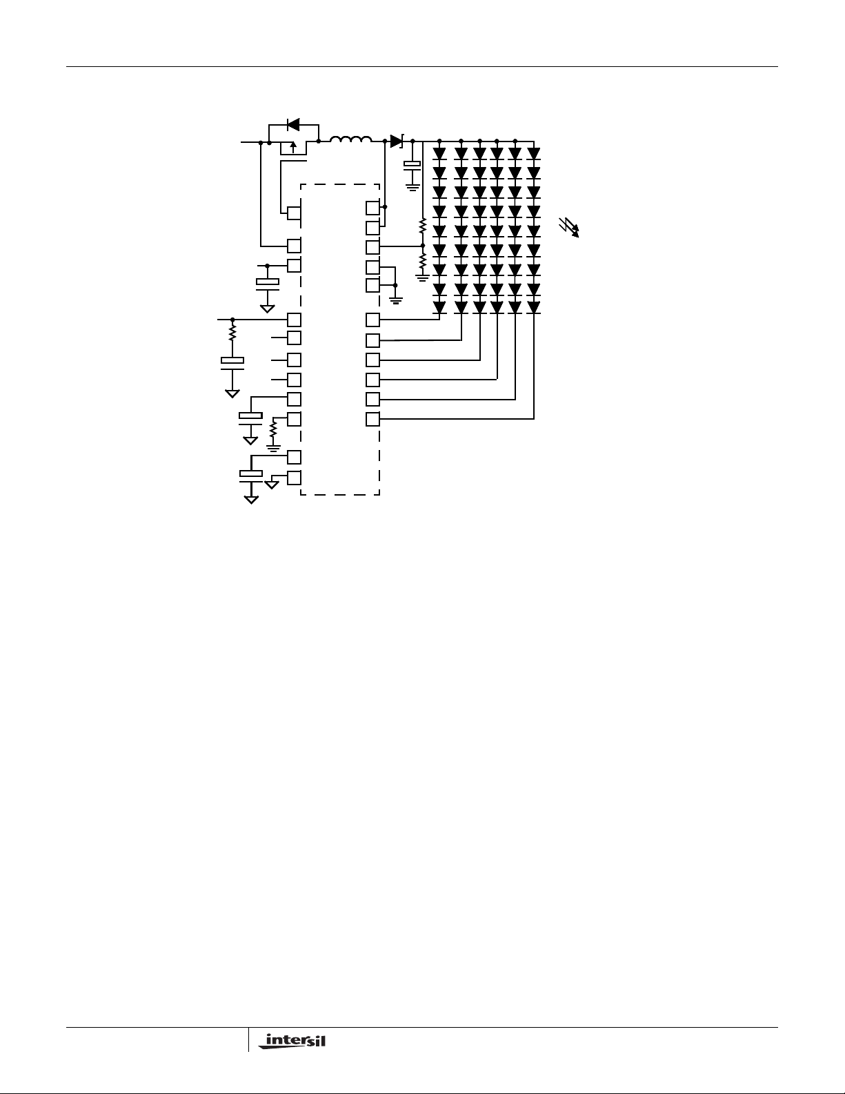
Typical Application Circuit
VBL+ = 6V TO 24V
21
23
24
ISL97635A
FAULT
VIN
VDC
LX
LX
OVP
PGND
PGND 18
ISL97635A
= 34.5V, 30mA PER STRING
V
OUT
19
20
16
17
22
1
2
6
4
11
3
5
COMP
SMBCLK
SMBDAT
PWMI/EN
PWMO
RSET
FPWM
GND
IIN0
IIN1
IIN2
IIN3
IIN4
IIN5
15
14
13
12
10
9
2
FN6564.2
December 22, 2008
Block Diagram
VBL+ = 6V TO 24V
ISL97635A
34.5V, 30mA PER STRING
(6 x 9 = 54 WHITE LEDS)
SMBCLK
SMBDAT
PWMI
PWMO
VDC
f
PWM
COMP
RSET
GND
VIN
VIN
REG
OSC AND
RAMP
COMP
LED PWM
CONTROL
INTERFACE
INTERFACE
+
+
-
-
SMBUS
FAULT
FAULT/STATUS
REGISTER
Σ = 0
ILIMIT
IMAX
GM
AMP
REFERENCE
GENERAT OR
REGISTERS
PWM BRIGHTNESS CONTROL
DEVICE CONTROL
FAULT/STATUS
IDENTIFICATION
DC BRIGHTNESS CONTROL
CONFIGURATION
LOGIC
HIGHEST VF
STRING
DETECT
+
+
-
-
PWM/OC/SC
AM
ISL97635A
FET
DRIVER
OC, SC
DETECT
OC, SC
DETECT
FAULT/STATUS
REGISTER
+
+
-
-
LX
LX
OVP
IIN0
IIN5
TEMP
SENSOR
FAUL T/STATUS
REGISTER
PGND
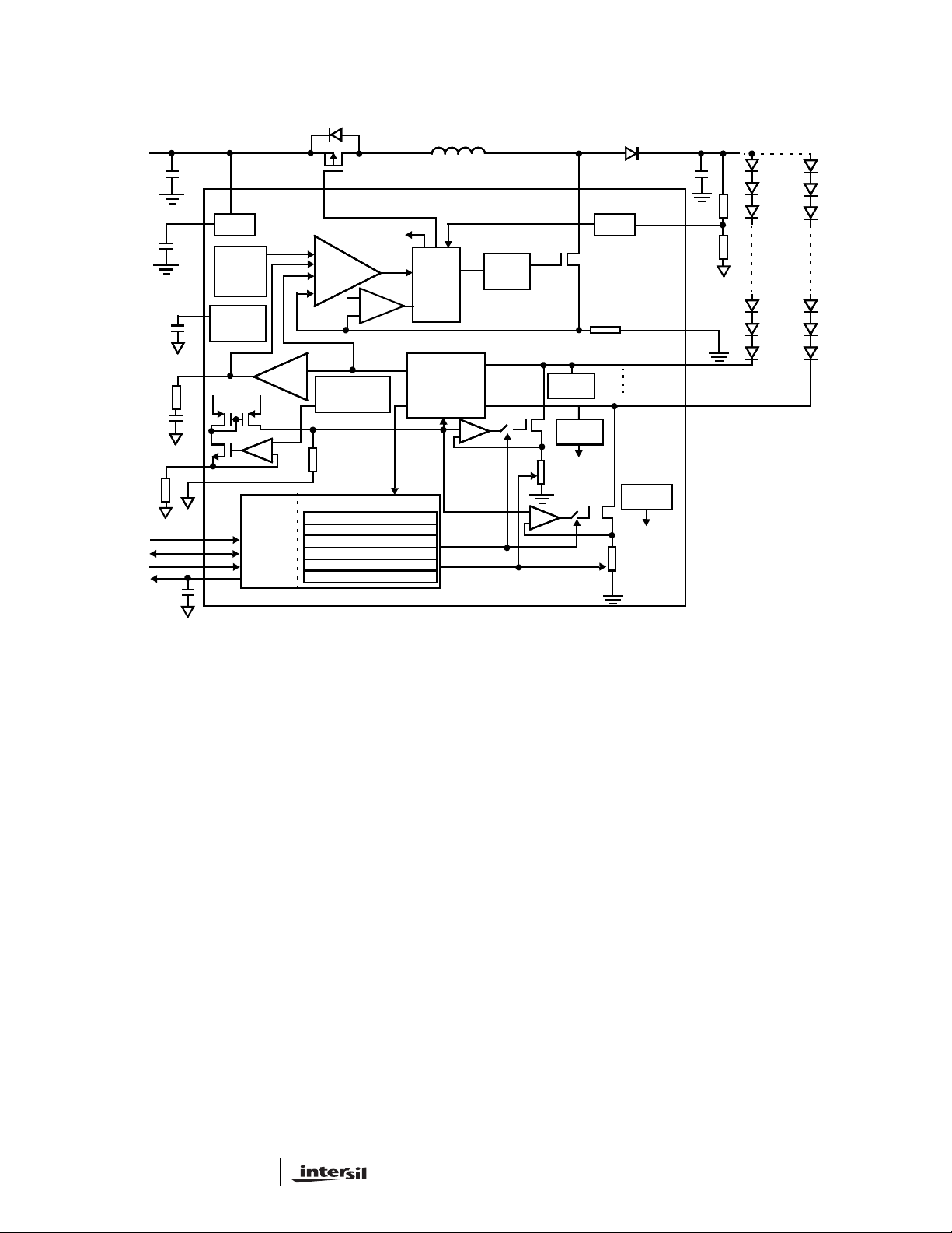
FIGURE 1. ISL97635A BLOCK DIAGRAM
3
FN6564.2
December 22, 2008
ISL97635A
Absolute Maximum Ratings (T
VIN, FAULT . . . . . . . . . . . . . . . . . . . . . . . . . . . . . . . . . .-0.3V to 24V
VDC, COMP, RSET . . . . . . . . . . . . . . . . . . . . . . . . . . . -0.3V to 6.5V
SMBCLK, SMBDAT, FPWM, PWMO, EN/PWM . . . . . -0.3V to 6.5V
OVP, IIN0 - IIN5 . . . . . . . . . . . . . . . . . . . . . . . . . . . . . . .-0.3V to 28V
LX. . . . . . . . . . . . . . . . . . . . . . . . . . . . . . . . . . . . . . . . . .-0.3V to 36V
PGND. . . . . . . . . . . . . . . . . . . . . . . . . . . . . . . . . . . . . -0.3V to +0.3V
Above voltage ratings are all with respect to GND pin
= +25°C) Thermal Information
A
Thermal Resistance (Typical, Notes 1, 2) θ
24 Ld QFN . . . . . . . . . . . . . . . . . . . . . . 39 2
Thermal Characterization (Typical, Note 3) PSI
24 Ld QFN . . . . . . . . . . . . . . . . . . . . . . . . . . . . . . . . ~0.7
Maximum Continuous Junction Temperature . . . . . . . . . . . .+125°C
Storage Temperature . . . . . . . . . . . . . . . . . . . . . . .-65°C to +150°C
Pb-free Reflow Profile . . . . . . . . . . . . . . . . . . . . . . . . .see link below
(°C/W) θJC (°C/W)
JA
(°C/W)
JT
http://www.intersil.com/pbfree/Pb-FreeReflow.asp
Operating Conditions
Temperature Range . . . . . . . . . . . . . . . . . . . . . . . . . .-40°C to +85°C
IMPORTANT NOTE: All parameters having Min/Max specifications are guaranteed. Typical values are for information purposes only. Unless otherwise noted, all tests
are at the specified temperature and are pulsed tests, therefore: T
CAUTION: Do not operate at or near the maximum ratings listed for extended periods of time. Exposure to such conditions may adversely impact product reliability and
result in failures not covered by warranty.
NOTES:
is measured in free air with the component mounted on a high effective thermal conductivity test board with “direct attach” features. See T ech
1. θ
JA
Brief TB379.
2. For θ
3. PSI
, the “case temp” location is the center of the exposed metal pad on the package underside assumed under ideal case temperature.
JC
is the junction-to-top thermal resistance. If the package top temperature can be measured, with this rating then the die junction temperature
JT
can be estimated more accurately than the θ
JC
4. Limits established by characterization and are not production tested.
Electrical Specifications All specifications below are tested at T
otherwise noted. Parameters with MIN and/or MAX limits are 100% tested at +25°C, unless otherwise
specified. Temperature limits established by characterization and are not production tested.
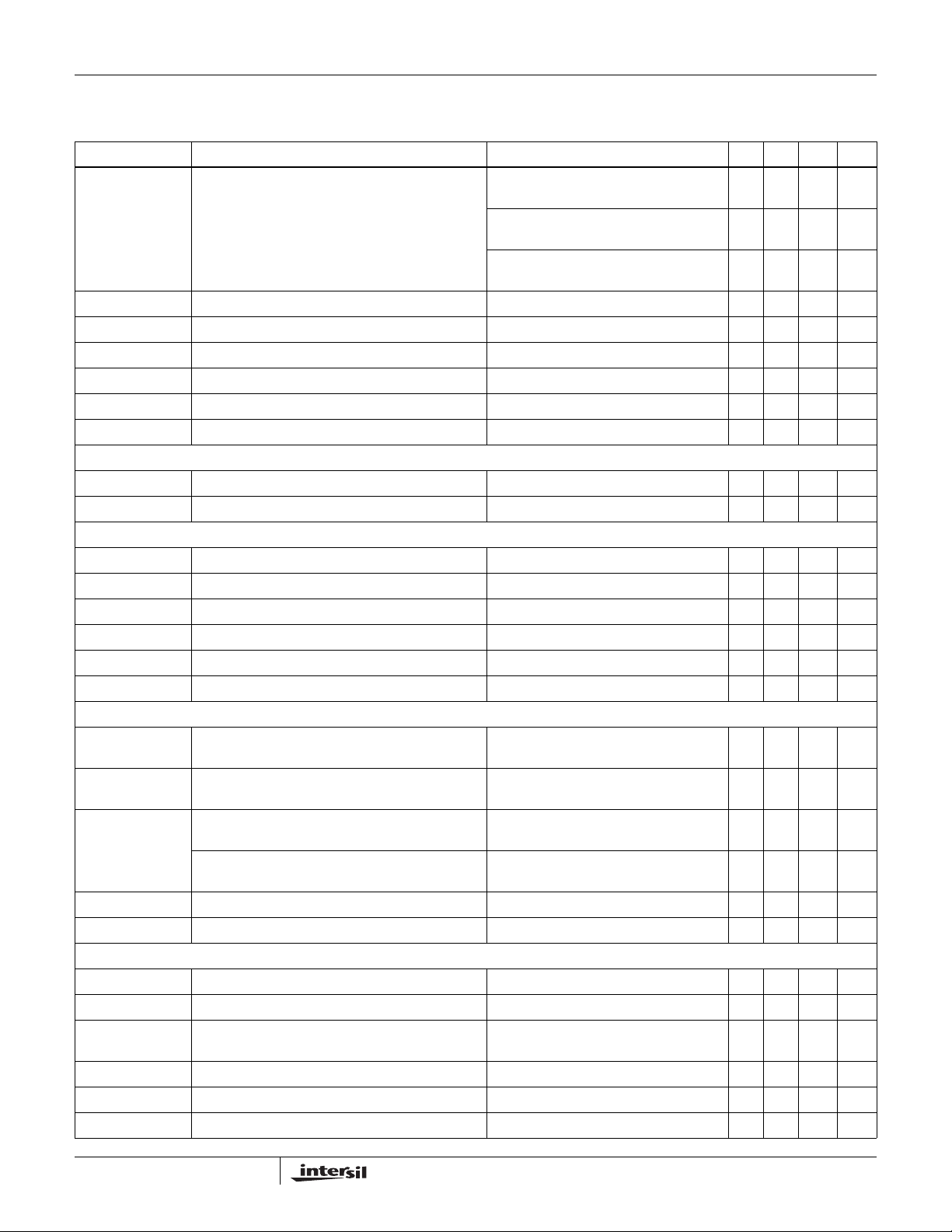
PARAMETER DESCRIPTION CONDITION MIN TYP MAX UNIT
GENERAL
VIN Backlight Supply Voltage ≤ 9 LEDs per channel (3.5V/30mA type) 6 24 V
IVIN_STBY VIN Shutdown Current 5µA
V
OUT
V
UVLO
V
UVLO_HYS
REGULATOR
V
DC
I
VDC_STBY
I
VDC
V
LDO
SS Soft-Start 1ms
ENmin Minimum Enable Signal 40 µs
BOOST
SWILimit Boost FET Current Limit T
r
DS(ON)
Output Voltage 34.5 V
Undervoltage Lockout Threshold 2.45 2.8 V
Undervoltage Lockout Hysteresis 300 mV
LDO Output Voltage VIN >6V 5.0 5.5 V
Standby Current EN/PWM = 0V 20 µA
Active Current EN/PWM = 5V 10 mA
VDC LDO Dropout Voltage VIN > 5.5V, 30mA 30 200 mV
Internal Boost Switch ON-Resistance 130 260 mΩ
= TC = T
J
A
and θJC thermal resistance ratings.
= -40°C to +85°C; VIN = 12V, EN = 5V, R
A
= +25°C 2.3 3.2 A
A
= -40°C to +85°C 2.2 A
T
A
= 36.6kΩ, unless
SET
4
FN6564.2
December 22, 2008
ISL97635A
Electrical Specifications All specifications below are tested at T
otherwise noted. Parameters with MIN and/or MAX limits are 100% tested at +25°C, unless otherwise
= -40°C to +85°C; VIN = 12V, EN = 5V, R
A
= 36.6kΩ, unless
SET
specified. Temperature limits established by characterization and are not production tested. (Continued)
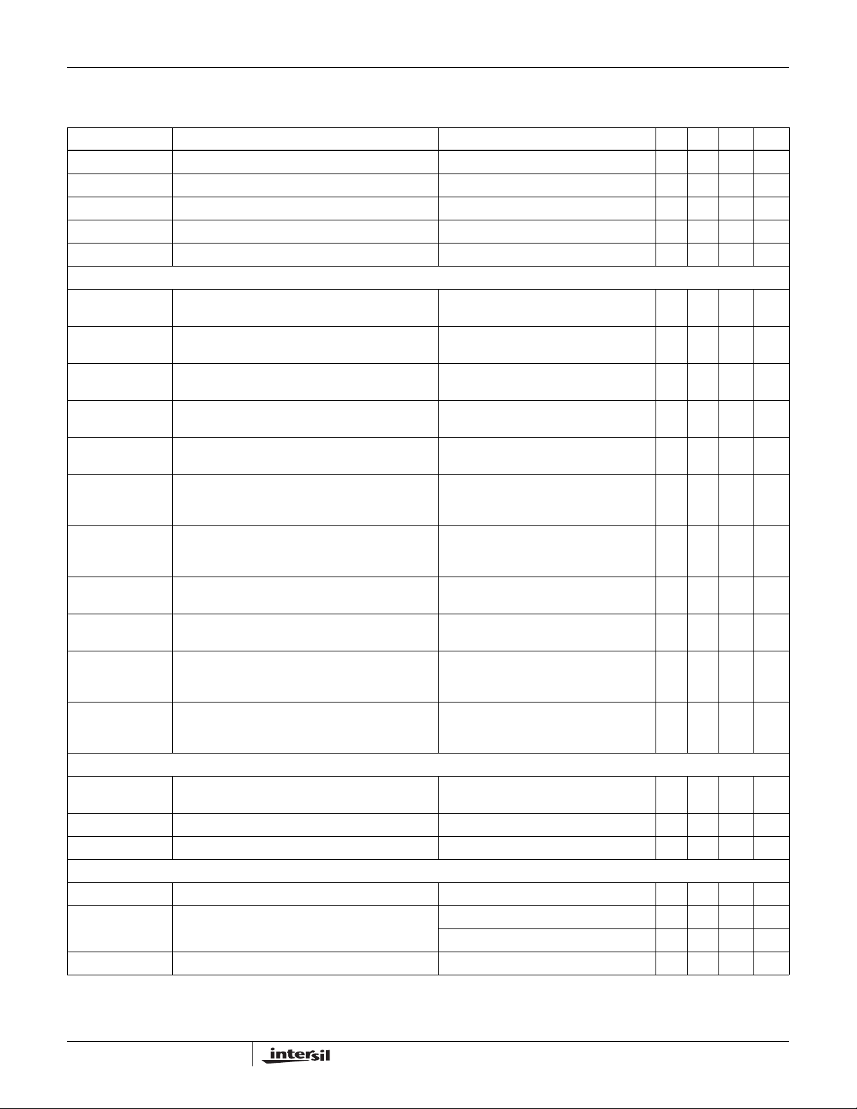
PARAMETER DESCRIPTION CONDITION MIN TYP MAX UNIT
Eff_peak Peak Efficiency VIN = 18V, 54 LEDs, 20mA each, L = 8.2µH
ΔI
OUT
D
max
D
min
F
OSC_hi
F
OSC_lo
/ΔV
with DCR 106mΩ, T
= 12V, 54 LEDs, 20mA each, L = 8.2µH
V
IN
with DCR 106mΩ, T
= 6V , 54 LEDs, 20mA each, L = 8.2µH
V
IN
with DCR 106mΩ, T
IN
Line Regulation 0.1 %
Boost Maximum Duty Cycle 82 %
Boost Minimum Duty Cycle 7%
LX Frequency Register 0x08, fSW = 1 1.0 1.2 1.3 MHz
LX Frequency Register 0x08, fSW = 0 550 600 650 kHz
= +25°C
A
= +25°C
A
= +25°C
A
91 %
88 %
86 %
ILX_leakage LX Leakage Current VLX = 36V, EN = 0 10 µA
REFERENCE
I
MATCH
I
ACC
Channel-to-Channel Current Matching I
Current Accuracy ±3 %
= 30mA, BRT = 255 -3.5 ±1 +3.5 %
OUT
FAULT DETECTION
V
SC
Short Circuit Threshold Reg0x08 = 0x0F or 0x0B Reg0x00 = 0xFF 7.8 8 8.8 V
Reg0x08 = 0x0E or 0x0A Reg0x00 = 0xFF 2.8 3.1 3.8 V
V
temp_acc
V
OVPlo
OVP
OVP
hys
fault
Over-Temperature Threshold Accuracy 5 °C
Overvoltage Limit on OVP Pin 1.17 1.2 1.23 V
OVP Hysteresis 20 mV
OVP Short Detection Fault Level 300 mV
SMBus INTERFACE
VIL Guaranteed Range for Data, Clock Input Low
0.8 V
Voltage
VIH
Guaranteed Range for Data, Clock Input High
2.1 VDD V
Voltage
VOL SMBus Data Line Logic Low Voltage with 1.1kΩ
Series Resistor from Data Bus to SMBDAT pin
SMBus Data Line Logic Low Voltage without Series
= 350µA 0.4 V
I
PULLUP
I
= 4mA 0.17 V
PULLUP
Resistor from Data Bus to SMBDAT Pin
I
LEAK
V
DD
Input Leakage on SMBData/SMBClk -1 1 µA
Nominal Bus Voltage 3V to 5V ±10% 2.7 5.5 V
SMBus TIMING SPECIFICATIONS (Note 4)
f
SMB
t
BUF
t
HD:STA
t
SU:STA
t
SU:STO
t
HD:DAT
SMBus Clock Frequency 10 100 kHz
Bus Free Time between STOP and ST ART Condition 4.7 µs
Hold Time after (Repeated) START Condition. After
4.0 µs
this Period, the First Clock is Generated.
Repeated Start Condition Setup Time 4.7 µs
Stop Condition Setup Time 4.0 µs
Data Hold Time 300 ns
5
FN6564.2
December 22, 2008
ISL97635A
Electrical Specifications All specifications below are tested at T
otherwise noted. Parameters with MIN and/or MAX limits are 100% tested at +25°C, unless otherwise
= -40°C to +85°C; VIN = 12V, EN = 5V, R
A
= 36.6kΩ, unless
SET
specified. Temperature limits established by characterization and are not production tested. (Continued)
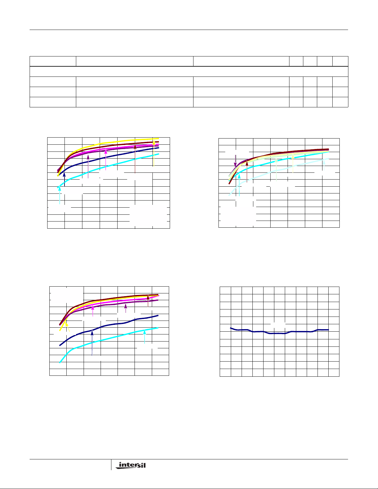
PARAMETER DESCRIPTION CONDITION MIN TYP MAX UNIT
t
SU:DAT
t
LOW
t
HIGH
t
F
t
R
Data Setup Time 250 ns
Clock Low Period 4.7 µs
Clock High Period 4.0 50 µs
Clock/Data Fall Time 300 ns
Clock/Data Rise Time 1000 ns
GENERAL TIMING SPECIFICATIONS (Note 4)
t
1
t
2
t
3
Minimum Setup Time Between VIN Rising above
VUVLO with EN = 1 and SMBus Communications
Minimum Setup Time Between EN Going High with
V
above VUVLO and SMBus Communications
IN
Minimum Time Between VIN Rising above VUVLO
EN = 1, TA = +25°C, VDC capacitor < 10µF 80 µs
> VUVLO, TA= +25°C,
V
IN
VDC capacitor < 10µF
80 µs
EN = 1, TA = +25°C 4.5 ms
with EN = 1 to SMBus BL CTRL On
t
4
t
5
t
6
Minimum Time Between EN Going High with VIN
above VUVLO to SMBus BL CTRL On
Minimum Time for LED Output to Respond to SMBus
Data at any Levels
Response Time Between Backlight CTRL Off with
Boost Not Switching to Backlight CTRL On with
VIN > VUVLO, TA = +25°C 4.5 ms
VIN > VUVLO, EN = 1, TA = +25°C 5 µs
V
> VUVLO, EN = 1, TA = +25°C 5 µs
IN
Boost Switching
t
7
Response Time Between Backlight CTRL On with
Boost Switching to Backlight CTRL Off with Boost
V
> VUVLO, EN = 1, TA = +25°C 5 µs
IN
Not Switching
t
8
t
9
t
10
LED Channel Short Circuit Fault Detection to Status
Register Data Ready
V
to Status Register Data Ready
Short Circuit Detection During Operation
OUT-GND
Time Between VIN Rising Above VUVLO with
EN = 1 and V
Short being Reported in
OUT-GND
VIN > VUVLO, EN = 1, TA = +25°C, LEDs
Active
VIN > VUVLO, EN = 1, TA = +25°C, Fault
FET used
EN = 1, VDC capacitor < 10µF , T
Fault FET used.
= +25°C,
A
6ms
5µs
30 ms
Status Register
t
11
Time Between EN Going High with VIN Above
VUVLO and a V
Status Register
Short being Reported in
OUT-GND
V
> VUVLO, VDC capacitor < 10µF,
IN
T
= +25°C, Fault FET used.
A
30 ms
CURRENT SOURCES
V
headroom
Dominant Channel Current Source Headroom at IIN
I
= 20mA, TA = +25°C 100 mV
LED
Pin
V
RSET
I
LEDmax
Voltage at RSET Pin R
Maximum LED Current Per Channel R
= 36.6kΩ 680 700 720 mV
SET
= 20.9kΩ 35 mA
SET
PWM GENERATOR (Note 4)
FPWM Generated PWM Frequency C
DPWM Duty Cycle of Generated PWM (DC-to-PWM) V
t
MAX_PWM_OFF
Maximum PWMI Off-Time Before Shutdown EN/PWMI toggles 28 ms
= 27nF, C
FPWM
= 0.3V CFPWM = 27nF 90 %
PWMO
= 1.1V CFPWM = 27nF 10 %
V
PWMO
= 220nF 200 Hz
PWMO
6
FN6564.2
December 22, 2008
ISL97635A
Electrical Specifications All specifications below are tested at T
otherwise noted. Parameters with MIN and/or MAX limits are 100% tested at +25°C, unless otherwise
= -40°C to +85°C; VIN = 12V, EN = 5V, R
A
= 36.6kΩ, unless
SET
specified. Temperature limits established by characterization and are not production tested. (Continued)
PARAMETER DESCRIPTION CONDITION MIN TYP MAX UNIT
FAULT PIN
I
FAULT
V
FAULT
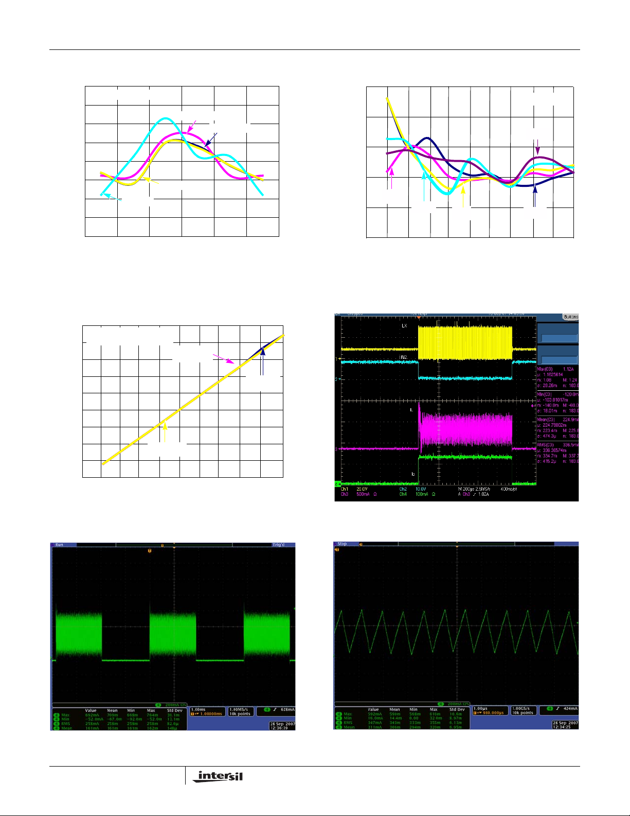
Fault Pull-down Current VIN = 12V 10 18 30 µA
FAULT Clamp Voltage With Respect to VIN VIN = 12, V
IN
- V
7.5 V
FAULT
IlxStart-up LX Start-up Current VDC = 5.2V 1 2.7 7 mA
Typical Performance Curves
92
90
88
86
84
82
80
78
76
EFFICIENCY (%)
74
72
9S6P - 6V
70
68
66
0 20 40 60 80 100 120 140
9S6P - 12V
7S6P - 6V
7S6P - 12V
(mA)
I
O
7S6P - 18V
9S6P - 18V
L = 8.2µH
IHLP-2525BD-01
DCR = 106mΩ
I
= 3A
SAT
FIGURE 2. EFFICIENCY, L = 8.2µH WITH DCR = 106mΩ,
C
= 4x4.7µF/50V
O
92
90
88
7S6P - 12V
86
84
82
80
78
76
EFFICIENCY (%)
74
72
L = 10µH
70
IHLP-2525BD-01
DCR = 129m
68
I
SAT
66
0 20 40 60 80 100 120 140
7S6P - 6V
= 2.5A
7S6P - 18V
Ω
9S6P - 18V
9S6P - 12V
(mA)
I
O
9S6P - 6V
FIGURE 3. EFFICIENCY, L = 10µH WITH DCR = 129mΩ,
C
= 4x4.7µF/50V
O
92
L = 10µH
90
DCR ~ 500mΩ
<1mm HEIGHT
88
86
84
82
80
7S6P - 18V
78
76
EFFICIENCY (%)
74
72
70
68
66
0 20 40 60 80 100 120 140
7S6P - 12V
7S6P - 6V
I
O
9S6P - 12V
(mA)
9S6P - 18V
9S6P - 6V
FIGURE 4. 3 EFFICIENCY, L = 10µH WITH DCR = 500mΩ,
1mm, C
= 4x4.7µF/50V
O
7
1.2
1.0
0.8
0.6
0.4
0.2
0.0
-0.2
-0.4
-0.6
CURRENT VARIATION (%)
-0.8
-1.0
-1.2
4 6 8 101214161820222426
20mA
V
IN
(V)
FIGURE 5. CURRENT REGULATION
December 22, 2008
FN6564.2
Typical Performance Curves (Continued)
ISL97635A
0.020
0.015
0.010
0.005
-0.005
CURRENT MATCHING
-0.010
-0.015
-0.020
6P9S = 54 LEDs
12V/1mA
12V/20mA
0
6V/20mA
6V/1mA
Ch 0 Ch 1 Ch 2 Ch 3 Ch 4 Ch 5
CHANNELS
FIGURE 6. CHANNEL-TO-CHANNEL CURRENT MATCHING
180
6 CHANNELS
9 LEDs PER CHANNEL
160
140
120
100
80
60
40
TOTAL OUTPUT CURRENT (mA)
20
0
0 102030405060708090100
PWM DUTY CYCLE (%)
VIN = 12V
VIN = 6V
V
= 18V
IN
FIGURE 8. PWM DIMMING LINEARITY
1.0
VIN = 12V
0.9
20kHz
0.8
0.7
CURRENT MATCHING (%)
0.6
0.5
200Hz
10kHz
0 0.1 0.2 0.3 0.4 0.5 0.6 0.7 0.8 0.9 1.0
1kHz
PWM DUTY CYCLE
100Hz
FIGURE 7. CURRENT MATCHING vs DUTY CYCLE vs
DIMMING FREQUENCY
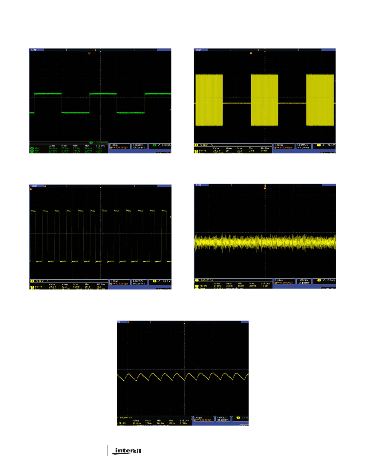
FIGURE 9. LX, IIN, IL AND LO
FIGURE 10. IL AT 50% PWM DIMMING
8
FIGURE 11. I
ZOOM IN AT PWM DIMMING ZOOM IN
L
December 22, 2008
FN6564.2
Typical Performance Curves (Continued)
ISL97635A
FIGURE 12. I
FIGURE 14. LX ZOOM IN AT 50% DIMMING
AT 50% PWM DIMMING
LED
FIGURE 13. LX AT 50% PWM DIMMING
FIGURE 15. RIPPLE VOLTAGE
FIGURE 16. RIPPLE VOLTAGE ZOOM IN
9
FN6564.2
December 22, 2008
 Loading...