®
www.BDTIC.com/Intersil
ISL97634
Data Sheet March 7, 2008
White LED Driver with Wide PWM
Dimming Range
The ISL97634 represents an efficient and highly integrated
PWM boost LED driver that is suitable for 1.8” to 3.5” LCDs
that employ 2 to 7 white LEDs for backligh ti n g. With
integrated Schottky diode, OVP, and wide range of PWM
dimming capability , the ISL97634 provides a simple, reliable,
and flexible solution to the backlight designers.
The ISL97634 features a wide range of PWM dimming
control capability. It allows dimming frequency as low as DC
to 32kHz beyond audible spectrum. The ISL97634 also
features a feedback disconnect switch to prevent the output
from being modulated by the PWM dimming signal that
minimizes system disturbance.
The ISL97634 is available in the 8 Ld TDFN (2mmx3mm)
package. There are 14V , 18V, and 26V OVP options that are
suitable for 3 LEDS, 4 LEDs, and 7 LEDs (3.5V/20mA type)
backlight applications respectively. The ISL97634 is
specified for operation over the -40°C to +85°C ambient
temperature at input voltage from 2.4V to 5.5V.
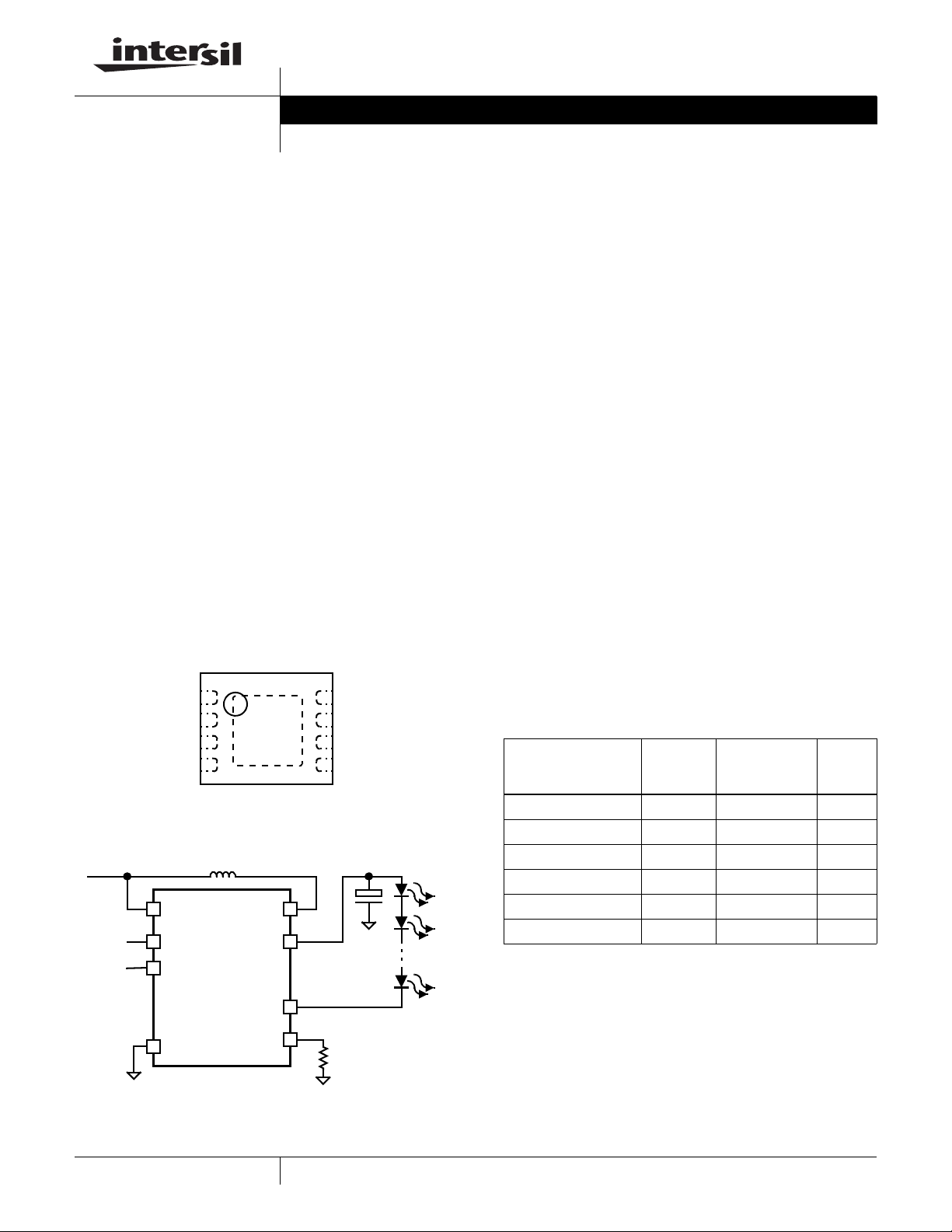
Pinout
ISL97634
(8 LD TDFN)
TOP VIEW
GND
VIN
PWM/EN
NC
1
2
3
4
8
7
6
5
LX
VOUT
FBSW
FB
Typical Application Circuit
VIN
PWM/EN
NC
GND
10µH or 22µH
LX
VOUT
FBSW
FB
VIN
FN6264.3
Features
• Drives Up to 7 LEDs in Series (3.5V/20mA type)
• OVP (14V , 18V, and 26V for 3, 4 and 7 LEDs Applications)
• PWM Dimming Control From DC to 32kHz
• Output Disconnect Switch
• Integrated Schottky Diode
• 2.4V to 5.5V Input
• 85% Efficiency
• 1.4MHz Switching Frequency Allows Small LC
• 1µA Shutdown Current
• Internally Compensated
• 8 Ld TDFN (2mmx3mm)
• Pb-Free (RoHS Compliant)
Applications
• LED Backlighting for:
- Cell phones
- Smartphones
-MP3
-PMP
- Automotive Navigation Panel
- Portable GPS
Ordering Information
PART
NUMBER
(Note)
ISL97634IRT14Z-T ELE 8 Ld 2x3 TDFN L8.2x3A
ISL97634IRT14Z-TK ELE 8 Ld 2x3 TDFN L8.2x3A
ISL97634IRT18Z-T ELF 8 Ld 2x3 TDFN L8.2x3A
ISL97634IRT18Z-TK ELF 8 Ld 2x3 TDFN L8.2x3A
ISL97634IRT26Z-T ELG 8 Ld 2x3 TDFN L8.2x3A
ISL97634IRT26Z-TK ELG 8 Ld 2x3 TDFN L8.2x3A
*Please refer to TB347 for details on reel specifications
NOTE: These Intersil Pb-free plastic packaged products employ
special Pb-free material sets; molding compounds/die attach
materials and 100% matte tin plate PLUS ANNEAL - e3 termination
finish, which is RoHS compliant and compatible with both SnPb and
Pb-free soldering operations. Intersil Pb-free products are MSL
classified at Pb-free peak reflow temperatures that meet or exceed
the Pb-free requirements of IPC/JEDEC J STD-020..
PART
MARKING
PACKAGE
(Pb-free)
Tape & Reel
PKG.
DWG.
#
1
CAUTION: These devices are sensitive to electrostatic discharge; follow proper IC Handling Procedures.
1-888-INTERSIL or 1-888-468-3774
| Intersil (and design) is a registered trademark of Intersil Americas Inc.
All other trademarks mentioned are the property of their respective owners.
Copyright Intersil Americas Inc. 2006-2008. All Rights Reserved

ISL97634
www.BDTIC.com/Intersil
Absolute Maximum Ratings (T
Input Voltage (V
LX Voltage . . . . . . . . . . . . . . . . . . . . . . . . . . . . . . . . . . .-0.3V to 28V
FBSW Voltage . . . . . . . . . . . . . . . . . . . . . . . . . . . . . . . .-0.3V to 28V
All Other Pins. . . . . . . . . . . . . . . . . . . . . . . . . . . . . . . . . .-0.3V to 6V
) . . . . . . . . . . . . . . . . . . . . . . . . . . . . .-0.3V to 6V
IN
Operating Conditions
Temperature Range . . . . . . . . . . . . . . . . . . . . . . . . . .-40°C to +85°C
CAUTION: Do not operate at or near the maximum ratings listed for extended periods of time. Exposure to such conditions may adversely impact product reliability and
result in failures not covered by warranty.
IMPORTANT NOTE: All parameters having Min/Max specifications are guaranteed over temperature of -40°C to +85°C unless otherwise stated. Typ values are for
information purposes only at TJ = TC = TA = +25°C.
NOTE:
1. θ
is measured in free air with the component mounted on a high effective thermal conductivity test board with “direct attach” features. See
JA
Tech Brief TB379.
2. For θ
, the “case temp” location is the center of the exposed metal pad on the package underside.
JC
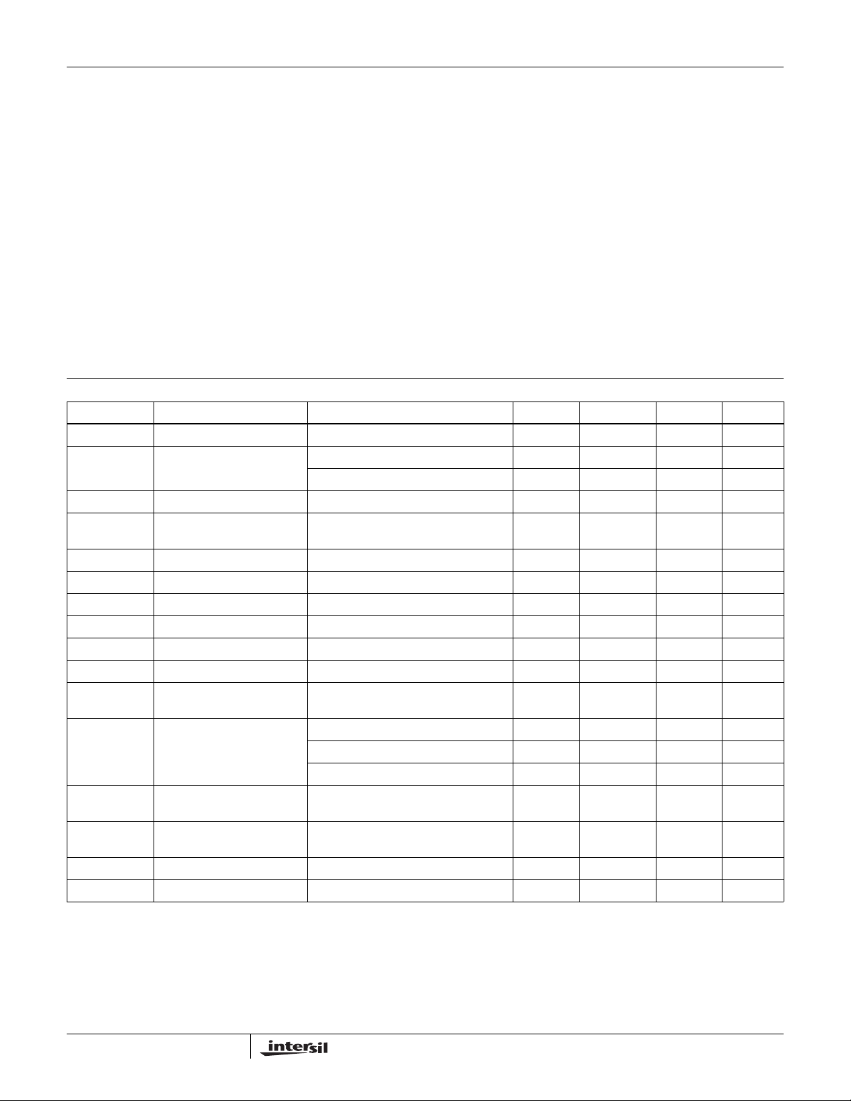
Electrical Specifications V
PARAMETER DESCRIPTION CONDITION MIN TYP MAX UNIT
V
IN
I
IN
f
SW
DMAX Maximum Switching Duty
I
LIM
R
SW(LX)
ILEAK LX Switch Leakage Current VLX = 28V 0.01 1 µA
VFB Feedback Voltage 90 95 100 mV
IFB FB Pin Bias Current VFB = 95mV 1 µA
R
SW(FBSW)
V
DIODE
OVP Overvoltage Protection ISL97634IRT14Z 14 V
VIL Logic Low Voltage of
VIH Logic High Voltage of
PWM_on Minimum PWM On-Time 1.5 µs
EN_delay EN to Vout Delay 200 µs
Supply Voltage 2.4 5.5 V
Supply Current PWM/EN = 3V, enabled, not switching 0.8 1.5 mA
Switching Frequency 1,300 1,450 1,600 kHz
Cycle
LX Current 400 470 mA
LX Switch ON-Resistance ILX = 100mA 900 mΩ
FBSW Switch ON-Resistance 10 Ω
Schottky Diode Forward
Voltage
PWM/EN
PWM/EN
= +25°C) Thermal Information
A
Thermal Resistance θ
8 Ld TDFN Package (Notes 1, 2). . . . . 77 12
Maximum Junction Temperature . . . . . . . . . . . . . . . . . . . . . .+125°C
Storage Temperature . . . . . . . . . . . . . . . . . . . . . . .-65°C to +150°C
Pb-free reflow profile . . . . . . . . . . . . . . . . . . . . . . . . . .see link below
http://www.intersil.com/pbfree/Pb-FreeReflow.asp
= V
IN
= 3V
PWM/EN
PWM/EN = 0V, disabled 1 µA
IDIODE = 100mA, TA = +25°C 600 850 mV
ISL97634IRT18Z 18 V
ISL97634IRT26Z 26 28 V
(°C/W) θ
JA
90 95 %
0.6 V
1.5 V
JC
(°C/W)
2
FN6264.3
March 7, 2008

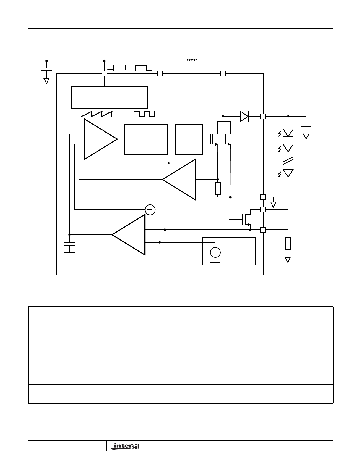
Block Diagram
www.BDTIC.com/Intersil
VIN (2.4V TO 5.5V)
CIN
ISL97634
L
VIN PWM/EN LX
1.4MHZ OSCILLATOR AND RAMP
GENERATOR
PWM
COMPARATOR
GM AMP
GM AMP
COMPENSATION
COMPENSATION
CONTROLLER
GM
AMPLIFIER
ISL97634
DRIVER
CURRENT
SENSE
95mV
VOUT
COUT
FET PWM LOGIC
2 LEDs to 7 LEDS
GND
FBSW
PWM/EN
FB
BANDGAP
REFERENCE
GENERATOR
RSET
Pin Description
PIN NUMBER PIN NAME DESCRIPTION
1 GND Ground Pin. Conn ect to local grou nd.
2 VIN In put Supply Pin. Connect to the input supply voltage, the inductor and the input supply de coupling capacitor .
3 PWM/EN PWM or Enable Pin. Connect external PWM signal allows pulse width modulation current operation. Enable
signal allows peak current operation or disable signal shuts dow n th e de vice.
4 NC No Connect
5 FB Feedback Pin. Connect the sense resistor between FB and ground. The cathode of bot tom LED ca n also
be connected at this pin if the output current is not to b e P WMed.
6 FBSW FB Disconnect Switch. Connect to the cathode of the bottom LED if the output current to be PWMed.
7 VOUT Output Pin. Connect to the anode of the top LED and the output filter capacitor.
8 LX Switching Pin. Connect to inductor.
3
FN6264.3
March 7, 2008
 Loading...