


®
www.BDTIC.com/Intersil
ISL97631
Data Sheet December 21, 2005
White LED Boost Regulator With
Integrated Schottky Diode
The ISL97631 represents a high efficiency, constant
frequency PWM regulator with integrated boost diode and
FET. Designed for use in white LED driving applications, the
ISL97631 features efficiencies up to 85%. It operates at
1.35MHz switching frequency and operates from an input
voltage of between 2.7V and 5.5V. The maximum output
voltage of 27V enables the ISL97631 to drive up to 6 LEDs in
series. It is also possible to use the ISL97631 to drive LEDs
in series/parallel combination for applications requiring up to
15 LEDs.
Available in the 6 Ld TSOT package, the ISL97631 offers
high efficiency, constant frequency operation. It is specified
for operation over the -40°C to +85°C ambient temperature
range.
Pinout
ISL97631
(6 LD TSOT)
TOP VIEW
VOUT
1
6
VIN
FN7370.1
Features
• Up to 6 LEDs in series
• 27V maximum output
• 2.7V to 5.5V input
• Up to 85% efficient
• 1.35MHz constant frequency
• Enable/PWM dimming control
• Pb-free plus anneal available (RoHS compliant)
Applications
• LED backlighting
• Cell phones
•PDAs
• Handheld games
• MP3 players
•GPS
• Other handheld devices
GND
LX
2
3
5FB
ENAB
4
Ordering Information
PAR T
PAR T N UMBE R
ISL97631IHTZ-T7 (See Note) 631Z 3,000 7” 6 Ld TSOT (Pb-free) MDP0049
ISL97631IHTZ-T7A (See Note) 631Z 270 7” 6 Ld TSOT (Pb-free) MDP0049
NOTE: Intersil Pb-free plus anneal products employ special Pb-free material sets; molding compounds/die attach materials and 100% matte tin plate
termination finish, which are RoHS compliant and compatible with both SnPb and Pb-free soldering operations. Intersil Pb-free products are MSL
classified at Pb-free peak reflow temperatures that meet or exceed the Pb-free requirements of IPC/JEDEC J STD-020.
MARKING PCS.
TAPE &
REEL
PACKAGE
(TAPE AND REEL) PKG. DWG. #
1
CAUTION: These devices are sensitive to electrostatic discharge; follow proper IC Handling Procedures.
1-888-INTERSIL or 1-888-468-3774
| Intersil (and design) is a registered trademark of Intersil Americas Inc.
All other trademarks mentioned are the property of their respective owners.
Copyright Intersil Americas Inc. 2005. All Rights Reserved

ISL97631
www.BDTIC.com/Intersil
Absolute Maximum Ratings (T
Input Voltage (VIN) . . . . . . . . . . . . . . . . . . . . . . . . . . . . . -0.3V to +6V
LX, Vout Voltage . . . . . . . . . . . . . . . . . . . . . . . . . . . . .-0.3V to +27V
FB Voltage . . . . . . . . . . . . . . . . . . . . . . . . . . . . . . . . . . . -0.3V to +6V
ENAB Voltage . . . . . . . . . . . . . . . . . . . . . . . . . . . . . . . . -0.3V to +6V
Operating Temperature . . . . . . . . . . . . . . . . . . . . . . .-40°C to +85°C
= 25°C) Thermal Information
A
Thermal Resistance (Typical, Note 1) θJA (°C/W)
6 Ld TSOT . . . . . . . . . . . . . . . . . . . . . . . . . . . . . . . . 190
Maximum Junction Temperature (Plastic Package . . . . . . . . . 150°C
Maximum Storage Temperature Range. . . . . . . . . .-65°C to +150°C
Maximum Lead Temperature (Soldering, 10s). . . . . . . . . . . . +300°C
(TSOT - Lead Tips Only)
CAUTION: Stresses above those listed in “Absolute Maximum Ratings” may cause permanent damage to the device. This is a stress only rating and operation of the
device at these or any other conditions above those indicated in the operational sections of this specification is not implied.
IMPORTANT NOTE: All parameters having Min/Max specifications are guaranteed over the specified temperature range. All parameters are based on pulsed tests,
therefore: T
= TC = T
J
A
NOTE:
1. θ
is measured with the component mounted on a high effective thermal conductivity test board in free air. See Tech Brief TB379 for details.
JA
Electrical Specifications V
= 3V, V
IN
= 3V, TA = -40°C to 85°C unless otherwise specified.
ENAB
PARAMETER DESCRIPTION CONDITION MIN TYP MAX UNIT
V
IN-MIN
V
IN-MAX
V
I
FB
I
FB
IN
Minimum Operating Voltage V
Maximum Operating Voltage V
Feedback Voltage 80 100 120 mV
FB Pin Bias Current 100 nA
Supply Current ENAB = 3V, output not switching 0.6 1.0 mA
OUT
OUT
= 16V, I
= 25V, I
= 20mA 2.7 V
LED
= 20mA 5.5 V
LED
ENAB = 0V 1 µA
F
D
OSC
MAX
Switching Frequency 0.8 1.35 1.8 MHz
Maximum Duty Cycle TA = 25°C 85 90 %
82 90 %
I
LIM
Switch Current Limit TA = 25°C 280 350 mA
250 350 mA
r
DS(ON)
I
LEAK(LX)
I
LEAK(VOUT)
V
DIODE
V
ENAB-HI
V
ENAB-LO
I
ENAB
/∆V
∆I
LED
Eff Efficiency I
Switch On Resistance ILX = 100mA 750 mΩ
Switch Leakage Current VLX = 27V, Vout = 27V 0.01 1 µA
Diode Leakage Current V
LX-V
Diode Forward Voltage I
OUT
= 27V 0.01 1 µA
OUT
= 100mA, TA = 25°C 0.75 0.9 V
DIODE
ENAB Voltage High 2.5 V
ENAB Voltage Low 0.6 V
ENAB Pin Bias Current 1µA
Line Regulation VIN = 2.7V to 5V 0.2 %/V
IN
= 20mA, 3 LEDs 85 %
LED
2
FN7370.1
December 21, 2005
Typical Application
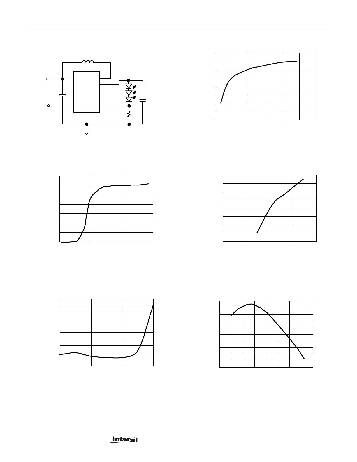
www.BDTIC.com/Intersil
L1
22µH
V
IN
2.7V~5.5V
C1
1µF
OFF/ON
V
IN
ISL97631
ENAB
V
OUT
GND
LX
FB
R
4.75Ω
FIGURE 1. TYPICAL APPLICATION CIRCUIT FIGURE 2. EFFICIENCY vs LED CURRENT (VIN = 4V)
Typical Performance Curves
SET
LEDs
C2
0.22µF
ISL97631
90
22µH, V
85
80
75
70
65
EFFICIENCY (%)
60
55
50
0 5 10 15 20 25 30
IN
= 4V
I
LED
(mA)
700
600
500
400
300
Iq (µA)
200
100
0
024
VIN (V)
6
FIGURE 3. QUIESCENT CURRENT vs VIN (ENAB = hi)
18.33
18.32
18.31
18.30
18.29
18.28
(mA)
O
I
18.27
18.26
18.25
18.24
18.23
2.5 3.5 4.5 5.5
(V)
V
IN
FIGURE 5. LINE REGULATION FIGURE 6. SWITCHING FREQUENCY vs TEMPERATURE
18.244
18.242
18.240
18.238
18.236
(mA)
O
I
18.234
18.232
18.230
18.228
0 5 10 15 20
(V)
V
OUT
FIGURE 4. LOAD REGULATION (V
1.37
1.36
1.35
1.34
1.33
1.32
1.31
1.30
FREQUENCY (MHz)
1.29
1.28
1.27
-60 -40 -20 0 20 40 60 80 100
TEMPERATURE (°C)
IN
= 4V)
3
FN7370.1
December 21, 2005

Block Diagram
www.BDTIC.com/Intersil
Vin Enable LX
Vin Enable LX
1.35MHz
1.2MHz Oscillator and Ramp
1.2MHz Oscillator and Ramp
Generator
Generator
PWM
PWM
Comparator
Comparator
GM Amp
GM Amp
Compensation
Compensation
ISL97631
PWM Logic
PWM Logic
Controller
Controller
GM
GM
Amplifier
Amplifier
ISL97631
ISL97631
FET
FET
Driver
Driver
Current
Current
Sense
Sense
-
-
95mV
95mV
Bandgap
Bandgap
Reference
Reference
Generator
Generator
Vout
Vout
GND
GND
FB
FB
FIGURE 7. ISL97631 BLOCK DIAGRAM
Pin Descriptions
PIN
NUMBER
1 VOUT Output Pin. Connect to the anode of the top
2 GND Ground Pin. Connect to local ground.
3 LX Switching Pin. Connect to inductor.
4 ENAB Enable Pin. Connect to enable signal to turn-on
5 FB Feedback Pin. Connect to the cathode of
6 VIN Input Supply Pin. Connect to the input supply
PIN
NAME DESCRIPTION
LED and the output filter capacitor .
or off the device.
bottom LED and the sense resistor.
voltage, the inductor and the input supply
decoupling capacitor.
Detailed Description
The ISL97631 uses a constant frequency, current mode
control scheme to provide excellent line and load
regulation. It can drive up to 6 LEDs in series or 15 LEDs in
parallel/series configuration, with efficiencies of up 85%.
The ISL97631 operates from an input voltage of 2.7V to
5.5V and can boost up to 27V.
Steady-State Operation
The ISL97631 operates with constant frequency PWM. The
switching frequency is around 1.35MHz. Depending on the
input voltage, inductance, number of LEDs and the LED
current, the converter operates in either continuous
conduction mode or discontinuous conduction mode. Both
are normal. The forward current of the LED is set using the
R
resistor. In steady state mode, this current is given by
SET
the equation:
V
I
LED
---------------=
R
FB
SET
(EQ. 1)
Shut-Down
When taken low the ENAB pin places the ISL97631 into
power down mode. When in power down, the supply current
is reduced to less than 1µA.
Dimming Control
PWM DIMMING
The ENAB pin also doubles as a brightness control. There
are two different possible dimming control methods. The
first dimming method is controlled through the duty-cycle of
the ENAB input PWM waveform, which can operate at
frequencies up to 1kHz. For frequencies greater than 1kHz,
see Analog Dimming. The LEDs operate at either zero or
full current. This is the PWM dimming control method. The
relationship between the average LED current and the
duty-cycle (D) of the ENAB pin’s waveform is as follows:
V
FB
average I
LED
---------------
R
SET
D⋅=
(EQ. 2)
4
FN7370.1
December 21, 2005

ISL97631
www.BDTIC.com/Intersil
The magnitude of the PWM signal should be higher than the
minimum ENAB voltage high. The bench PWM dimming test
results are shown in Figure 8. In the test, two PWM
frequencies 400Hz and 1kHz are chosen to compare the
linear dimming range. It is clear that there is a wider linear
dimming range for the lower PWM frequency than for the
higher one, due to the self discharge of the output capacitor
through the LEDs during the low ENAB periods. To achieve
a better linearity with high frequencies an NMOS FET can be
placed between the FB pin and the LED stack, with its gate
driven by the same signal as ENAB. This acts to prevent self
discharge of the output capacitor during the off periods. In
the PWM dimming test, the output capacitor is 0.22µF.
20
18
16
14
12
10
(mA)
O
I
8
6
4
2
0
020406080100
FIGURE 8. PWM DIMMING LINEAR RANGE (FOR 400Hz AND
1kHz PWM FREQUENCIES CONDITION,
C
OUT
1kHz
400Hz
DUTY-CYCLE (%)
= 0.22µF)
ANALOG DIMMING
The second dimming method applies a variable DC voltage
(V
) at FB pin (see Figure 9) to adjust the LED current. As
Dim
the DC dimming signal voltage increases above V
voltages drop on R
on R
I
LED
decreases. Thus, the LED current decreases.
SET
VFBR1R2+()V
------------------------------------------------------------ --------------= (EQ. 3)
and R2 increase and the voltage drop
1
⋅–⋅
R⋅
DimR1
SET
R
2
FB
, the
The DC dimming signal voltage can be a variable DC voltage
or a DC voltage generated by filtering a high frequency PWM
control signal.
As brightness is directly proportional to LED currents, V
Dim
may be calculated for any desired “relative brightness” (F)
using Equation 4.
V
Dim
R
-------
R
2
⋅⋅=
V
FB
1
R
1
1
------- F–+
R
2
(EQ. 4)
L1
22µH
V
IN
2.7V~5.5V
C1
1µF
OFF/ON
FIGURE 9. ANALOG DIMMING CONTROL APPLICATION
CIRCUIT
V
LX
LX
IN
V
OUT
ISL97631
ENAB FB
GND
R2
R1
3.3k
LEDs
C2
0.22µF
R
SET
4.75Ω
V
Dim
The analog dimming circuit can be tailored to a desired
relative brightness for different V
ranges using
Dim
Equation 5.
R
-------------------------------------------------------------- -----=
2
Where V
V
Dim_maxVFB
V
Dim_max
–()R1•[]
1F
–()•[]
FB
min
is the maximum V
voltage and F
Dim
(EQ. 5)
is
min
the minimum relative brightness (i.e., the brightness with
V
Dim_max
i.e., V
i.e., V
applied).
Dim_max
Dim_max
= 5V, F
= 1V, F
= 10% (i.e., 0.1), R2 = 189k
min
= 10% (i.e., 0.1), R2 = 35k
min
Open-Voltage Protection
In some applications, it is possible that the output is
opened, e.g. when the LEDs are disconnected from the
circuit or the LEDs fail. In this case the feedback voltage
will be zero. The ISL97631 will then switch to a high duty
cycle resulting in a high output voltage, which may cause
the LX pin voltage to exceed its maximum 27V rating. To
implement overvoltage protection, a zener diode Dz and a
resistor R
voltage on the LX pin as shown in Figure 10. It is clear that
as the zener is turned on, due to the overvoltage, the zener
diode’s current will set up a voltage on R
voltage is applied on FB pin as the feedback node. This
feedback will prevent the output from reaching the
overvoltage condition. In the overvoltage protection circuit
design, the zener voltage should be larger than the
maximum forward voltage of the LED string.
can be used at the output and FB pin to limit the
1
and R
1
SET
and this
Where F = I
(dimmed)/I
LED
(undimmed).
LED
These equations are valid for values of R1 and R2 such that
both R1>>RSET and R2>>RSET.
5
FN7370.1
December 21, 2005

ISL97631
www.BDTIC.com/Intersil
L1
V
IN
2.7V~5.5V
1µF
OFF/ON
C1
22µH
V
IN
ISL97631
ENAB
V
OUT
GND
LX
FB
Dz
R1
R
SET
4.75Ω
LEDs
C2
0.22µF
FIGURE 10. LED DRIVER WITH OVERVOLTAGE
PROTECTION CIRCUIT
Components Selection
The input capacitance is typically 0.22µF. The output
capacitor should be in the range of 0.22µF to 1µF. X5R or
X7R type of ceramic capacitors of the appropriate voltage
rating are recommended. The output capacitor value affects
PWM dimming performance. Lower output capacitor values
increase the range of PWM dimming. However, the ripple
voltage will be greater for lower values.
When choosing an inductor, make sure the average and
peak current ratings are adequate by using the following
formulas (80% efficiency assumed):
I
⋅
LEDVOUT
I
LAVG
I
LPKILAVG
∆
I
Where:
•
• L is the inductance in H.
•f
---------------------------------=
⋅
0.8 V
IN
1
-- -
∆⋅+=
I
L
2
V
INVOUTVIN
---------------------------------------------------=
L
LV
⋅⋅
∆I
is the peak-to-peak inductor current ripple in Amps
L
is the switching frequency, typically 1.35MHz
OSC
–()⋅
OUTfOSC
(EQ. 6)
(EQ. 7)
(EQ. 8)
90%
22µH, V
85%
80%
2LED
75%
70%
65%
EFFICIENCY (%)
60%
55%
50%
0 5 10 15 20 25 30
3LED
IN
= 4V
6LED
4LED
5LED
I
LED
(mA)
FIGURE 11. EFFICIENCY CURVE WITH 2, 3, 4, 5 AND 6 LEDs
LOAD
White LED Connections
One leg of LEDs connected in series will ensure brightness
uniformity. The 27V maximum output voltage specification
enables up to 6 LEDs to be placed in series.
In order to drive more LEDs, series/parallel connections are
used. A current mirror circuit (as shown in Figure 12) should
be used to balance LED currents.
Parallel strings of LEDs may draw significantly different
currents due to manufacturing and temperature differences.
For correct operation of the current mirror circuit, the total
voltage between FB pin and the top of the primary LED
string must be equal to or greater than the other strings. To
ensure this, a small value resistor may be inserted between
FB pin and the primary LED string.
D1
D1
L1
L1
V
IN
2.7V~5.5V
C1
OFF/ON
VDD
VIN
LX
LX
ISL97631
EL7630
VOUT
ENAB FB
ENAB FB
GND
GND
C2
LEDs
R
SET
The ISL97631 supports a wide range of inductance values
(22µH~82µH). For lower inductor values or lighter loads, the
boost inductor current may become discontinuous. For high
boost inductor values, the boost inductor current will be in
FIGURE 12. LEDs IN SERIES/PARALLEL WITH MIRROR
continuous mode.
The demo board efficiency bench test results are shown in
Figure 11. The input voltage is 4V and curves are shown for
2, 3, 4, 5 and 6 LEDs (boost inductor L = 22µH).
6
CURRENT BALANCE
FN7370.1
December 21, 2005

PCB Layout Considerations
www.BDTIC.com/Intersil
The layout is very important for the converter to function
properly. R
and GND pins. Longer traces to the LEDs are OK. Similarly,
the supply decoupling cap and the output filter cap should be
as close as possible to the V
The heat of the IC is mainly dissipated through the GND pin.
Maximizing the copper area connected to this pin is
preferable. In addition, a solid ground plane is always helpful
for the EMI performance.
The demo board is a good example of layout based on the
principle. Please refer to the ISL97631 Application Brief for
the layout.
must be located as close as possible to the FB
SET
and V
IN
OUT
pins.
ISL97631
7
FN7370.1
December 21, 2005

Package Outline
www.BDTIC.com/Intersil
ISL97631
All Intersil U.S. products are manufactured, assembled and tested utilizing ISO9000 quality systems.
Intersil Corporation’s quality certifications can be viewed at www.intersil.com/design/quality
Intersil products are sold by description only. Intersil Corporation reserves the right to make changes in circuit design, software and/or specifications at any time without
notice. Accordingly, the reader is cautioned to verify that data sheets are current before placing orders. Information furnished by Intersil is believed to be accurate and
reliable. However, no responsibility is assumed by Intersil or its subsidiaries for its use; nor for any infringements of patents or other rights of third parties which may result
from its use. No license is granted by implication or otherwise under any patent or patent rights of Intersil or its subsidiaries.
For information regarding Intersil Corporation and its products, see www.intersil.com
8
FN7370.1
December 21, 2005
 Loading...