

®
www.BDTIC.com/Intersil
ISL96017
Data Sheet April 17, 2006
128-Tap DCP, 16kbit EEPROM, and I2C
Serial Interface
This device integrates a 128-tap digitally controlled
potentiometer, 16kbit of EEPROM, and a 2-wire I
interface. The device is powered by a single 3.3V supply.
The potentiometer is available with total resistance of either
10kΩ or 50kΩ.
The memory is organized in 128 pages of 16 bytes each, to
reduce total programming time. All programming signals are
generated on-chip.
The potentiometer is implemented with a combination of
CMOS switches and resistor elements. The position of the
wiper can be stored in non-volatile memory an d th en be
recalled upon a subsequent power-up. The three terminals
of the potentiometer are available for use as either a variable
resistor or a resistor divider.
2
C serial
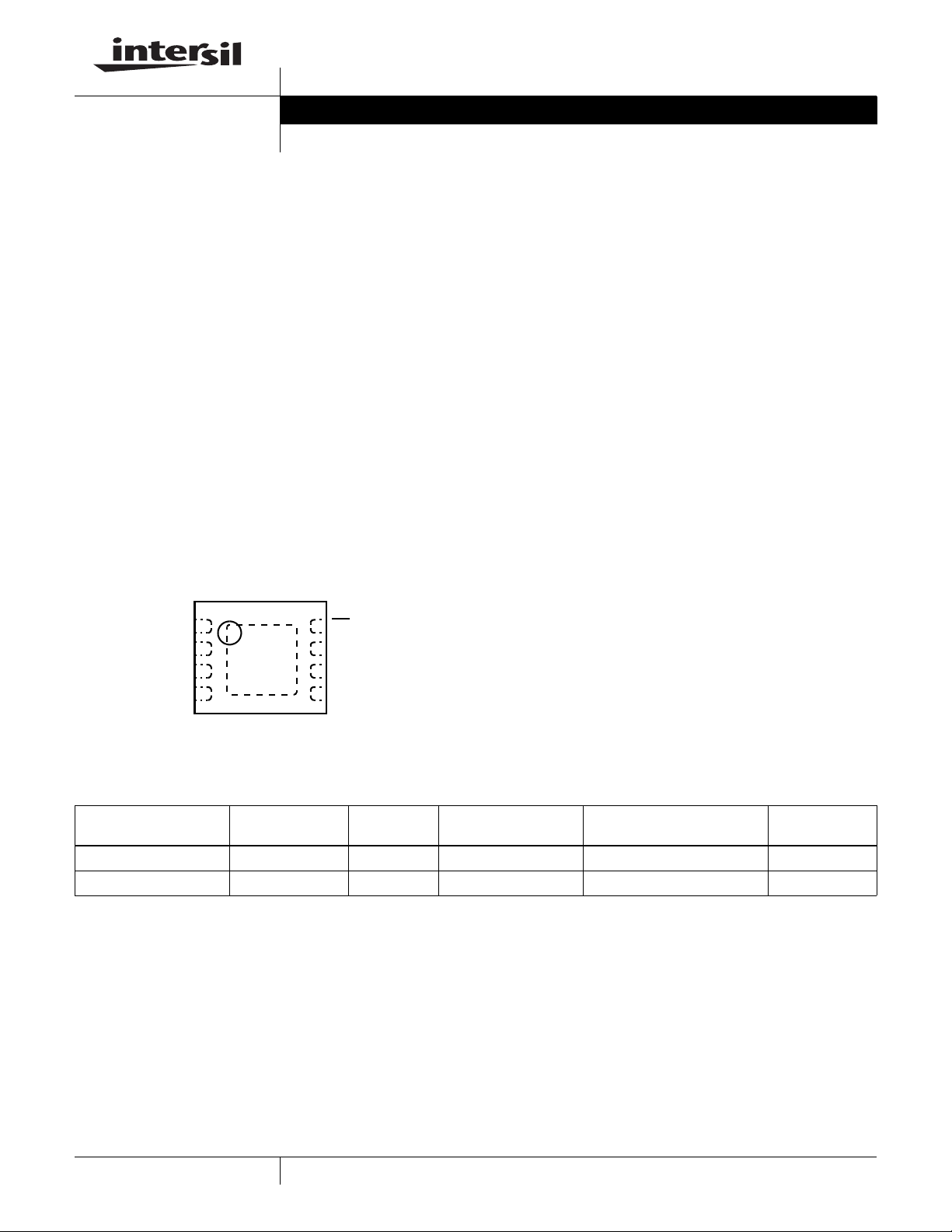
Pinout
ISL96017
(8 LD TDFN)
TOP VIEW
FN8243.1
Features
• Integrated Digitally Controlled Potentiometer
- 128-Tap Positions
-10kΩ, 50kΩ Total Resistance
- Monotonic Over Temperature
- Non-Volatile Wiper Position Storage
- 0 to VDD Terminal Voltage
2
C Serial Interface
•I
• 16kbit EEPROM
- 50 Years Retention @ ≤ 55°C
- 1,000,000 Cycles Endurance
• Single 3.3
• 3mm x 3mm Thin DFN Package – 0.8mm Max Thickness,
0.65mm Pitch
• Pb-Free Plus Anneal Available (RoHS Compliant)
±0.3V Supply
RH
RW
RL
VDD
1
2
3
4
8
WP
SCL
7
SDA
6
GND
5
Ordering Information
TEMP.
PART NUMBER PART MARKING R
ISL96017WIRT8Z* (Note) 96017WIZ 10 -40 to 85 8 Ld 3x3 TDFN (Pb-free) L8.3x3A
ISL96017UIRT8Z* (Note) 96017UIZ 50 -40 to 85 8 Ld 3x3 TDFN (Pb-free) L8.3x3A
*Add "-TK" suffix for 1000 units tape and reel.
NOTE: Intersil Pb-free plus anneal products employ special Pb-free material sets; molding compounds/die attach materials and 100% matte tin plate
termination finish, which are RoHS compliant and compatible with both SnPb and Pb-free soldering operations. Intersil Pb-free products are MSL
classified at Pb-free peak reflow temperatures that meet or exceed the Pb-free requirements of IPC/JEDEC J STD-020.
TOTAL
(kΩ)
RANGE (°C) PACKAGE
PKG.
DWG. #
1
CAUTION: These devices are sensitive to electrostatic discharge; follow proper IC Handling Procedures.
1-888-INTERSIL or 1-888-468-3774
| Intersil (and design) is a registered trademark of Intersil Americas Inc.
All other trademarks mentioned are the property of their respective owners.
Copyright Intersil Americas Inc. 2005. All Rights Reserved
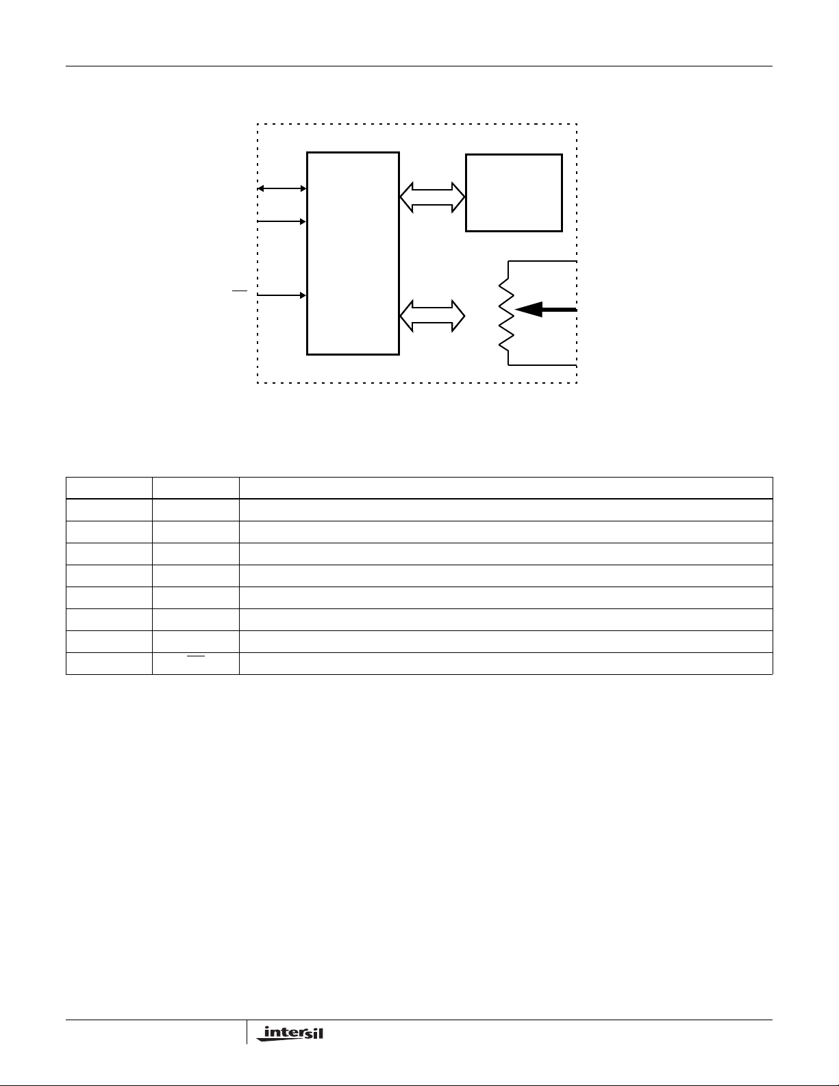
Block Diagram
www.BDTIC.com/Intersil
ISL96017
SDA
SCL
WP
POWER-UP,
INTERFACE,
AND
CONTROL
LOGIC
Pin Descriptions
PIN SYMBOL DESCRIPTION
1 RH “High” terminal of the DCP
2 RW “Wiper” terminal of the DCP
3 RL “Low” terminal of the DCP
4 VDD Power supply
5 GND Ground
6 SDA Open drain serial interface data input/output
7 SCL Open drain serial interface clock input
8WP
Hardware write protection pin. Active low. Prevents any “Write” operation to the device.
16kbit
EEPROM
RH
RW
RL
2
FN8243.1
April 17, 2006
ISL96017
www.BDTIC.com/Intersil
Absolute Maximum Ratings Thermal Information
Storage Temperature: . . . . . . . . . . . . . . . . . . . . . . . .-65°C to 150°C
Note: All Voltages with Respect to GND
Voltage at SCL, SDA, WP
Voltage at RH, RW, RL: . . . . . . . . . . . . . . . . . . . . . . . GND to VDD
VDD . . . . . . . . . . . . . . . . . . . . . . . . . . . . . . . . . . . . . . . . -0.3V to 4V
Lead Temperature (Soldering, 10s): . . . . . . . . . . . . . . . . . . . .300°C
Wiper Current. . . . . . . . . . . . . . . . . . . . . . . . . . . . . . . . . . . . . . ±6mA
ESD (MIL-STD-883B, Method 3014). . . . . . . . . . . . . . . . . . .>2000V
ESD (Machine Model) . . . . . . . . . . . . . . . . . . . . . . . . . . . . . . .>150V
CAUTION: Stresses above those listed under “Absolute Maximum Ratings” may cause permanent damage to the device. This is a stress rating only; the functional
operation of the device, at these or any other conditions above those listed in the op erational se ctions of th is specification, is not implied. Exposure to abso lute maximum
rating conditions for extended periods may affect device reliability.
Note:
θ
is measured in free air with the component mounted on a high effective thermal conductivity test board with “direct attach” features. See
1.
JA
Tech Brief TB379 for details.
: . . . . . . . . . . . . . . . . . . . . .-0.3V to 4V
Thermal Resistance (Typical, Note 1)
8 Ld TDFN Package. . . . . . . . . . . . . . . . . . . . . . . . . . . . . 90(°C/W)
Moisture Sensitivity (see Technical Brief TB363). . . . . . . . . .Level 2
Maximum Junction Temperature (Plastic Package). . . . . . . . . .150°C
Recommended Operating Conditions
Ambient Temperature . . . . . . . . . . . . . . . . . . . . . . . . .-40°C to 85°C
VDD Voltage for DCP Operation . . . . . . . . . . . . . . . . . . 3.0V to 3.6V
Wiper Current . . . . . . . . . . . . . . . . . . . . . . . . . . . . . . . -3mA to 3mA
Power Rating. . . . . . . . . . . . . . . . . . . . . . . . . . . . . . . . . . . . . . .5mW
Electrical Specifications Over recommended operating conditions unless otherwise stated. All voltages with respect to GND.
TYP
SYMBOL PARAMETER TEST CONDITIONS MIN
IccdSby Standby Current at VDD Serial interface in standby 10 µA
IccdRd Read Current at VDD Reading with 400kHz at SCL 1 mA
IccdWr Write Current at VDD Writing to EEPROM 5 mA
I
LkgDig
I
LkgDCP
VDDRamp VDD Power-Up Ramp Rate 0.2 V/ms
t
DCP
(Note 13)
t
D
CH/CW/CL
(Note 13)
R
Total
R
Wiper
DCP IN VOLTAGE DIVIDER MODE (0V at RL, VCC at RH; measured at RW unloaded)
FSerror
(Note 2, 3)
ZSerror
(Note 2, 4)
TC
(Note 7, 13)
DNL (Note 2, 5) Differential Non-Linearity Monotonic over all tap positions -0.75 0.75 LSB
INL (Note 2, 6) Integral Non-Linearity -1 1 LSB
Leakage Current at Pins SDA, SCL,
and WP
Leakage Current at RH, RW, RL Pin voltage from GND to VDD -1 1 µA
DCP Wiper Response Time SCL falling edge of last bit of DCP Data Byte to
Power-Up Delay VDD above 2.6V, to DCP Initial Value Register
RH, RW, RL Pin Capacitance 10 pF
Total Resistance W and U versions, respectively. TA =25°C.
R
Tolerance TA = 25°C. Measured between RH and RL pins. -20 20 %
Total
Wiper Resistance VDD = 3.3V @ 25°C. Wiper current = VDD/R
DCP Resolution 7Bits
Full-Scale Error U option -2 -1 0 LSB
Zero-Scale Error U option 0 1 2 LSB
Ratiometric Temperature
V
Coefficient
Pin voltage from GND to VDD -10 10 µA
wiper change
2
recall completed, and I
state
Measured between R
W option -5 -1 0 LSB
W option 0 1 5 LSB
DCP Register between 10 hex and 6F hex ±4 ppm/°C
C Interface in standby
and RL pins.
H
Total
(Note 1) MAX UNIT
1.5 µs
3ms
10, 50 kΩ
100 300 Ω
JA
θ
3
FN8243.1
April 17, 2006
ISL96017
www.BDTIC.com/Intersil
Electrical Specifications Over recommended operating conditions unless otherwise stated. All voltages with respect to GND. (Continued)
SYMBOL PARAMETER TEST CONDITIONS MIN
DCP IN RESISTOR MODE (Measurements between RH and RW with RL not connected)
(Note 8) Resistance Offset. U version - DCP Register set to 7F hex.
R
127
TC
(Note 11,13)
RDNL
(Note 8,9)
RINL
(Note 8,10)
EEPROM SPECS
(Note 12) Non-Volatile Write Cycle Time 6 12 ms
t
WC
SERIAL INTERFACE SPECS
V
IL
V
IH
Hysteresis SDA and SCL Input Buffer
V
OL
Cpin WP
f
SCL
t
IN
t
AA
t
BUF
t
LOW
t
HIGH
t
SU:STA
t
HD:STA
t
SU:DAT
t
HD:DAT
t
SU:STO
Resistance Temperature Coefficient ±100 ppm/°C
R
Resistance Differential NonLinearity
Resistance Integral Non-Linearity -1 1 MI
EEPROM Endurance 1,000,000 Cycles
EEPROM Retention At 55°C 50 Years
WP, SDA, and SCL Input Buffer
LOW Voltage
WP, SDA and SCL Input Buffer
HIGH Voltage
Hysteresis
SDA Output Buffer LOW Voltage,
Sinking 4mA
, SDA, and SCL Pin Capacitance 10 pF
SCL Frequency 400 kHz
Pulse Width Suppression Time at
SDA and SCL Inputs.
SCL Falling Edge to SDA Output
Data Valid
Time the Bus Must be Free Before
the Start of a New Transmission
Clock LOW Time Measured at the 30% of VDD crossing 1300 ns
Clock HIGH Time Measured at the 70% of VDD crossing 600 ns
START Condition Setup Time SCL rising edge to SDA falling edge. Both
STAR T Condition Hold Time From SDA falling edge crossing 30% of VDD to
Input Data Setup Time From SDA exiting the 30% to 70% of VDD
Input Data Hold Time From SCL rising edge crossing 70% of VDD to
STOP Condition Setup Time From SCL rising edge crossing 70% of VCC, to
Measured between R
W version - DCP Register set to 7F hex.
Measured between R
Any pulse narrower than the max spec is
suppressed
SCL falling edge crossing 30% of VDD, until
SDA exits the 30% to 70% of VDD window
SDA crossing 70% of VCC during a STOP
condition, to SDA crossing 70% of VDD during
the following START condition
crossing 70% of VDD
SCL falling edge crossing 70% of VDD
window, to SCL rising edge crossing 30% of
VDD
SDA entering the 30% to 70% of VDD window
SDA rising edge crossing 30% of VDD
and RW pins.
H
and RW pins.
H
00.52MI
-0.75 0.75 MI
-0.3 0.3*
0.7*
VDD
0.05*
VDD
00.4V
1300 ns
600 ns
600 ns
100 ns
0ns
600 ns
TYP
(Note 1) MAX UNIT
15MI
(Note 1)
(Note 1)
V
VDD
VDD
+0.3
50 ns
900 ns
V
V
4
FN8243.1
April 17, 2006

ISL96017
www.BDTIC.com/Intersil
Electrical Specifications Over recommended operating conditions unless otherwise stated. All voltages with respect to GND. (Continued)
SYMBOL PARAMETER TEST CONDITIONS MIN
t
HD:STO
STOP Condition Hold Time From SDA rising edge to SCL falling edge. Both
600 ns
crossing 70% of VDD
t
DH
Output Data Hold Time From SCL falling edge crossing 30% of VDD,
until SDA enters the 30% to 70% of VDD
0ns
window
t
R
t
F
SDA and SCL Rise Time From 30% to 70% of VDD 20+
0.1*Cb
SDA and SCL Fall Time From 70% to 30% of VDD 20+
0.1*Cb
Cb Capacitive Loading of SDA or SCL Total on-chip and off-chip 10 400 pF
Rpu SDA and SCL Bus Pull-Up Resistor
Off-Chip
Maximum is determined by t
For Cb = 400pF, max is about 2~2.5kΩ
and t
R
F
1kΩ
For Cb = 40pF, max is about 15~20kΩ
t
SU:WP
t
HD:WP
WP Setup Time Before START condition 600 ns
WP Hold Time After STOP condition 600 ns
NOTES:
2. Typical values are for T
3. LSB = (V(RW)
127
4. FSerror = (V(RW)
5. ZSerror = V(RW)
6. DNL = [(V(RW)
7. INL = [V(RW)
8. for i = 16 to 111, and T = -40°C to 85°C
TC
V
9. MI = (R
0
i
– i * LSB – V(RW)0]/LSB, for I = 1 to 127.
i
Max V RW()i()Min V RW()i()–[]
-----------------------------------------------------------------------------------------------
Max V RW()i()Min V RW()i()+()2⁄
– R
)/127. MI is minimum increment. R0 and R
127
= 25°C and VDD = 3.3V.
A
– V(RW)0)/127. V(RW)
– VDD)/LSB
127
/LSB
0
– V(RW)
)/LSB] – 1, for i from 1 to 127. i is the DCP Register setting.
i-1
and V(RW)0 are the voltage at pin RW for the DCP Register set to 7F hex and 00 hex respectively .
127
6
10
-----------------
×=
125° C
are the resistances between RH and RW with the DCP Register set to 00 hex and
127
7F hex, respectively.
– R
10. RDNL = (R
11. RINL = [R
12. ; for i = 1 to 111, and T = -40°C to 85°C
TC
13. t
WC
valid STOP condition at the end of a Write sequence of a I
i
Max Ri()Min Ri()–[]
--------------------------------------------------------------- -
R
Max Ri()Min Ri()+[]2⁄
is the minimum cycle time to be allowed for any non-volatile Write by the user, unless Acknowledge Polling is used. It is the time from a
)/MI – 1, for i from 1 to 111. i is the DCP Register setting.
i
i-1
– (MI * i) – R
]/MI, for i from 1 to 111.
127
6
110
×
-------------------
×=
125° C
2
C serial interface Write operation, to the end of the self-timed internal non-volatile
write cycle.
14. Parameter is not 100% tested.
TYP
(Note 1) MAX UNIT
250 ns
250 ns
I2C Timing Diagram
SCL
t
(INPUT TIMING)
(OUTPUT TIMING)
SDA
SDA
SU:STA
5
t
HD:STA
t
F
t
SU:DAT
t
HIGH
t
LOW
t
HD:DAT
t
R
t
SU:STO
t
t
DH
AA
t
BUF
FN8243.1
April 17, 2006

Typical Performance Curves
www.BDTIC.com/Intersil
ISL96017
140
WIPER RESISTANCE (Ω)
120
100
T = 25°C
80
60
40
20
0
0
20 40 60 80 100 120 140
TAP POSITION (DECIMAL)
VDD = 3.6V
VDD = 3.0V
FIGURE 1. WIPER RESISTANCE vs T AP POSITION
FOR 10kΩ (W)
0.2
0.15
0.05
INL (LSB)
-0.05
-0.15
T = 25°C
0.1
0
-0.1
-0.2
0 20 40 60 80 100 120 140
TAP POSITION (DECIMAL)
V
DD
VDD = 3.6V
= 3.0V
FIGURE 3. INL vs TAP POSITION FOR 10kΩ (W)
0.15
VDD = 3.0V
0.1
0.05
0
-0.05
-0.1
DNL (LSB)
-0.15
-0.2
T = 25°C
-0.25
0 20 40 60 80 100 120 140
= 3.6V
V
DD
TAP POSITION (DECIMAL)
FIGURE 2. DNL vs TAP POSITION FOR 10kΩ (W)
0.2
0.15
V
= 3.6V
DD
0.1
0.05
0
-0.05
RDNL (LSB)
-0.1
-0.15
-0.2
0 20 40 60 80 100 120 140
= 3.0V
V
DD
TAP POSITI ON (DECIMAL)
FIGURE 4. RDNL vs TAP POSITION FOR 10kΩ (W)
T = 25°C
0.4
0.3
0.2
0.1
0
RINL (LSB)
-0.1
-0.2
V
DD
-0.3
0 20 40 60 80 100 120 140
FIGURE 5.
= 3.6V
V
= 3.0V
DD
TAP POSITI ON (DECIMAL)
RINL vs TAP POSITION FOR 10kΩ (W)
6
T = 25°C
FN8243.1
April 17, 2006

Principles of Operation
www.BDTIC.com/Intersil
This device combines a DCP, 16kbit non-volatile memory,
and an I
between a host and the DCP and memory.
DCP Description
The DCP has 10kΩ or 50kΩ nominal total resistance and
128 taps. It is implemented with a combination of resistor
elements and CMOS switches. The physical ends of the
DCP, the RH and RL pins, are equivalent to the fixed
terminals of a mechanical potentiometer. The RW pin is
connected to intermediate nodes, and it is equivalent to the
wiper terminal of a mechanical potentiometer. The position
of the wiper terminal within the DCP is controlled by a 7-bit
volatile DCP Register. When the DCP Register contains all
zeroes (00 hex, or “R
its RL terminal. When the DCP Register contains all ones
(7F hex, or “R
terminal. As the value of the DCP Register increases from all
zeroes to all ones, the wiper moves monotonically from the
position closest to RL to the closest to RH. Therefore, the
resistance between RH and RW decreases monotonically
from R
increases monotonically from R
While the device is being powered up, the DCP Register is
reset to 40 hex (64 decimal). Soon after the power supply
voltage becomes large enough for reliable non-volatile
memory reading, the device reads the value stored on the
non-volatile Initial Value Register (IVR) and loads it into the
DCP Register.
2
C serial interface providing direct communication
”), its wiper terminal, RW, is closest to
0
”), its wiper terminal is closest to its RH
127
to R
0
, while the resistance between RW and RL
127
127
to R0.
ISL96017
controls the access to the DCP byte (See “Access to DCP
Register and IVR”). Bytes at addresses 7FC hex and 7FD
hex, are reserved, which means that they should not be
written, and their value should be ignored if they are read.
(See Table 1).
Access to DCP Register and IVR
The volatile DCP Register and the non-volatile (IVR) can be
read or written directly using the I
Address Byte 07FF hex.
The MSB of the byte at address 7FE hex is called
“OnlyVolatile” and controls the access to the DCP Register
and IVR. This bit is volatile and it’s reset to “0” at power up.
The Data Byte read from memory address 7FF hex, is from
the DCP register when the “OnlyVolatile” bit is “1”, and from
the IVR when this bit is “0”.
The Data Byte of a Write operation to memory address 7FF
hex is written only to the DCP Register when the
“OnlyVolatile” bit is “1”, and it’s written to both the DCP
Register and the IVR when this bit is “0”.
When writing to the “OnlyVolatile” bit at address 7FE hex,
the seven LSBs of the Data Byte must be all zeros.
Writing to address 7FE hex and 7FF hex can be done in two
Write operations, or one Write operation with two Data
Bytes.
See next sections for interface protocol description.
2
C serial interface, with
Memory Description
This device contains 2048 non-volatile bytes organized in
128 pages of 16 bytes each. This allows writing 16 bytes on
a single I
non-volatile write cycle. The memory is accessed by I
interface operations with addresses 000 hex through 7FF hex.
Bytes at addresses 000 hex through 7FB hex are available
to the user as general purpose memory. The byte at address
7FF hex, IVR, contains the initial value loaded at power-up
into the volatile DCP Register. The byte at address 7FE hex
2
C interface operation, followed by a single internal
TABLE 1. ISL96017 MEMORY MAP
2
C
Addres s Data B its Function
7FFh 0 D
6D5D4D3D2D1D0
7FEhOV0000000 Access Control
7FDh Res erved
7FCh Res erved
7FB h D
7D6D5D4D3D2D1D0
000h
Note: OV = “Only Volatile”. All other bits in register 7FEh must be 0.
IVR, DCP
General Purpos e M em ory
7
FN8243.1
April 17, 2006

ISL96017
www.BDTIC.com/Intersil
I2C Serial Interface
This device supports a bidirectional bus oriented protocol.
The protocol defines any device that sends data onto the
bus as a transmitter and the receiving device as the receiver.
The device controlling the transfer is a master and the
device being controlled is the slave. The master always
initiates data transfers and provides the clock for both
transmit and receive operations. Therefore, this device
operates as a slave device in all applications. All
communication over the I
sending the MSB of each byte of data first.
Protocol Conventions
Data states on the SDA line can change only during SCL
LOW periods. SDA state changes during SCL HIGH are
reserved for indicating START and STOP conditions (See
Figure 6). On power up, the SDA pin is in the input mode. All
2
I
C interface operations must begin with a START condition,
which is a HIGH to LOW transition of SDA while SCL is
HIGH. The device continuously monitors the SDA and SCL
lines for the START condition and does not respond to any
command until this condition is met (See Figure 6). A START
condition is ignored during the power up sequence and
during internal non-volatile write cycles. All I
operations must be terminated by a STOP condition, which
is a LOW to HIGH transition of SDA while SCL is HIGH (See
Figure 6). A STOP condition at the end of a Read operation,
or at the end of a Write operation to volatile bytes only
places the device in its standby mode. A STOP condition
during a Write operation to a non-volatile byte, initiates an
2
C interface is conducted by
2
C interface
internal non-volatile write cycle. The device enters its
standby state when the internal non-volatile write cycle is
completed.
An ACK, Acknowledge, is a software convention used to
indicate a successful data transfer. The transmitting device,
either master or slave, releases the SDA bus after
transmitting eight bits. During the ninth clock cycle, the
receiver pulls the SDA line LOW to acknowledge the
reception of the eight bits of data (See Figure 7). This device
responds with an ACK after recognition of a START
condition followed by a valid Identification Byte, and once
again after successful receipt of the Address Byte. This
device also responds with an ACK after receiving each Data
Byte of a Write operation. The master must respond with an
ACK after receiving each Data Byte of a read operation
except the last one. A valid Identification Byte contains 1010
as the four MSBs. The following three bits are the MSBs of
the memory address to be accessed. The LSB of the
Identification Byte is the Read/Write bit. Its value is “1” for a
Read operation, and “0” for a Write operation (See Table 2).
The complete memory address location to be accessed is a
11-bit word, since the memory has 2048 bytes. The eight
LSBs are in the Address Byte.
TABLE 2. IDENTIFICATION BYTE FORMAT
1010A10A9A8R/Wb
MSB LSB
SCL
SDA
SCL
SDA
START
DATA STABLE DATA CHANGE DATA STABLE
FIGURE 6. VALID DATA CHANGES, START AND STOP CONDITIONS
STOP
8
FN8243.1
April 17, 2006

SCL FROM MASTER
www.BDTIC.com/Intersil
ISL96017
81 9
SDA OUTPUT FROM
TRANSMITTER
SDA OUTPUT FROM
RECEIVER
START ACK
HIGH IMPEDANCE
FIGURE 7. ACKNOWLEDGE RESPONSE FROM RECEIVER
Write Operation
A Write operation requires a START condition, followed by a
valid Identification Byte, a valid Address Byte, one or more
Data Bytes, and a STOP condition (See Figure 8). After each
of the bytes, this device responds with an ACK. At this time,
if the operation is only writing to volatile registers, then the
device enters its standby state. If one or more Data Bytes
are to be written to non-volatile memory, the device begins
its internal write cycle to non-volatile memory. During this
cycle, the device ignores transitions at the SDA and SCL
pins, and the SDA output is at a high impedance state. When
the internal non-volatile write cycle is completed, the device
enters its standby state.
The memory is organized as 128 pages of 16 bytes each.
This allows writing 16 bytes on a single I
operation, followed by a single internal non-volatile write
cycle. The addresses of bytes within a page share the same
eight MSBs, and differ on the four LSBs. For example, the
first page is located at addresses 0 hex through F hex, the
second page is located at addresses 10 hex through 1F hex,
etc.
A Write operation with more than one Data Byte sends the
first Data Byte to the memory address indicated by the three
address bits of the Identification Byte plus the eight bits of
the Address Byte, the second Data Byte to the following
address, etc.
A single Write operation has to stay within a page. If the
Address Byte corresponds to the lowest address of a page,
then the Write operation can have anywhere from 1 to 16
Data Bytes. If the Address Byte corresponds to the highest
address of a page, then only one byte can be written with
that Write operation.
See “Access to DCP Register and IVR” for additional
information.
2
C interface
HIGH IMPEDANCE
respond to them with ACK, and instead, goes to its standby
state waiting for a new START condition.
A valid Identification Byte, Address Byte, and total number of
SCL pulses act as a protection of both volatile and nonvolatile registers.
During a Write sequence, Data Bytes are loaded into an
internal shift register as they are received. If the address bits
in the Identification Byte plus the bits in the Address Byte are
all ones, the Data Byte is transferred to the DCP Register at
the falling edge of the SCL pulse that loads the last bit (LSB)
of the Data Byte.
The STOP condition acts as a protection of non-volatile
memory. Non-volatile internal write cycles are started by
STOP conditions.
Read Operation
A Read operation consist of a three byte instruction followed
by one or more Data Bytes (See Figure 9). The master
initiates the operation issuing the following sequence: a
START, the Identification Byte with the R/W bit set to “0”, an
Address Byte which contains the LSBs of the memory
address, a second START, and a second Identification Byte
with the same address bits but with the R/W bit set to “1”.
After each of the three bytes, this device responds with an
ACK. Then this device transmits Data Bytes as long as the
master responds with an ACK during the SCL cycle following
the eighth bit of each byte. The master terminates the Read
operation (issuing a STOP condition) following the last bit of
the last Data Byte. The Data Bytes are from the memory
location indicated by an internal pointer. This pointer initial
value is determined by the address bits in the Identification
Byte plus the bits in the Address Byte in the Read operation
instruction, and increments by one during transmission of
each Data Byte.
Data Protection
The WP pin has to be at logic HIGH to perform any Write
operation to the device. When WP
device ignores Data Bytes of a Write operation, does not
is active (LOW) the
9
FN8243.1
April 17, 2006

ISL96017
www.BDTIC.com/Intersil
SIGNALS FROM
THE MASTER
SIGNAL AT SDA
SIGNALS FROM
SIGNALS
FROM THE
MASTER
SIGNAL AT SDA
SIGNALS FROM
THE SLAVE
THE SLAVE
S
T
A
R
ADDRESS WITH
T
1010
SLAVE
R/Wb=0
S
T
A
R
T
1010
0
SLAVE
ADDRESS
A
C
K
WRITE
ADDRESS
BYTE
0
A
C
K
FIGURE 8. WRITE SEQUENCE
S
T
A
ADDRESS
ADDRESS
BYTE
R
T
A
C
K
SLAVE
WITH
R/Wb=1
FIRST DATA BYTE
TO WRITE
A
C
K
READ
1
A
C
FIRST READ
K
DATA BYTE
LAST DATA BYTE
TO WRITE
A
C
K
A
A
C
C
K
K
S
T
O
P
A
C
K
LAST READ
DATA BYTE
S
T
A
O
C
P
K
FIGURE 9. READ SEQUENCE
Applications Information
The typical application diagram is shown on Figure 10. For
proper operation adding 0.1µF decoupling ceramic capacitor
to Vdd
is recommended. The capacitor value may vary
based on expected noise frequency of the design.
Vdd=3.3V
Rpu
Rpu
FIGURE 10. TYPICAL APPLICATION DIAGRAM FOR IMPLEMENTING ADJUSTABLE VOLTAGE REFERANCE
Vdd=3.3V
WP
SCL
SDA
ISL96017
0.1uF
Vdd=3.3V
RH
RW
RL
Vcc
0.1uF
Vout
R2
R1
10
FN8243.1
April 17, 2006

ISL96017
www.BDTIC.com/Intersil
Thin Dual Flat No-Lead Plastic Package (TDFN)
(DATUM B)
6
INDEX
AREA
(DATUM A)
NX L
8
NX (b)
5
SECTION "C-C"
A
6
INDEX
AREA
SEATING
PLANE
C
12
N
(A1)
D
TOP VIEW
SIDE VIEW
D2
D2/2
N-1
e
(Nd-1)Xe
REF .
BOTTOM VIEW
TERMINAL TIP
FOR EVEN TERMINAL/SIDE
2X
2X
ABC0.15
0.15
CB
L8.3x3A
8 LEAD THIN DUAL FLAT NO-LEAD PLASTIC PACKAGE
MILLIMETERS
SYMBOL
NOTESMIN NOMINAL MAX
A 0.70 0.75 0.80 -
E
A1 - 0.02 0.05 A3 0.20 REF -
b 0.25 0.30 0.35 5, 8
D 3.00 BSC -
D2 2.20 2.30 2.40 7, 8, 9
E 3.00 BSC -
E2 1.40 1.50 1.60 7, 8, 9
e 0.65 BSC -
k0.25 - - -
L 0.20 0.30 0.40 8
A3
//
A
0.10
0.08
C
C
N82
Nd 4 3
87
Rev. 3 11/04
NOTES:
1. Dimensioning and tolerancing conform to ASME Y14.5-1994.
2. N is the number of terminals.
NX k
3. Nd refers to the number of terminals on D.
4. All dimensions are in millimeters. Angles are in degrees.
E2
E2/2
5. Dimension b applies to the metallized terminal and is measured
between 0.15mm and 0.30mm from the terminal tip.
6. The configuration of the pin #1 identifier is optional, but must be
located within the zone indicated. The pin #1 identifier may be
NX b
5
0.10
BAMC
either a mold or mark feature.
7. Dimensions D2 and E2 are for the exposed pads which provide
improved electrical and thermal performance.
8. Nominal dimensions are provided to assist with PCB Land
Pattern Design efforts, see Intersil Technical Brief TB389.
C
L
L1
e
L
10
9. Compliant to JEDEC MO-WEEC-2 except for the “L” min
dimension.
All Intersil U.S. products are manufactured, assembled and tested utilizing ISO9000 quality systems.
Intersil Corporation’s quality certifications can be viewed at www.intersil.com/design/quality
Intersil products are sold by description only. Intersil Corporation reserves the right to make changes in circuit design, software and/or specifications at any time without
notice. Accordingly, the reader is cautioned to verify that data sheets are current before placing orders. Information furnished by Intersil is believed to be accurate and
reliable. However, no responsibility is assumed by Intersil or its subsidiaries for its use; nor for any infringements of patents or other rights of third parties which may result
from its use. No license is granted by implic atio n or other wise u nde r any p a tent or patent rights of Intersil or its sub sidi aries.
For information regarding Intersil Corporation and its products, see www.intersil.com
11
FN8243.1
April 17, 2006
 Loading...