

DATASHEET
0.84
0.85
0.86
0.87
0.88
0.89
0.90
0.91
0 5 10 15 20 25
VIN = 12V
VIN = 6V
VIN = 21V
0.82
0.83
0.84
0.85
0.86
0.87
0.88
0.89
0.90
0.91
0 5 10 15 20 25 30 35 40
VIN = 12V
VIN = 6V
VIN = 21V
0.84
0.85
0.86
0.87
0.88
0.89
0.90
0.91
0123456
VIN = 12V
VIN = 6V
VIN = 21V
ISL95859C
1+2+1 Voltage Regulator With Expanded Iccmax Register Range Supporting
Intel IMVP8 CFL/CNL CPUs
The ISL95859C provides a complete power solution for
Intel microprocessors supporting core, graphics, and
system agent rails and is compliant with Intel IMVP8™.
The controller provides control and protection for three
Voltage Regulator (VR) outputs. The VR A and VR C
outputs support 1-phase operation only, while VR B is
configurable for 2- or 1-phase operation. The
programmable address options for these three outputs
allow for maximum flexibility in support of the IMVP8
CPU. All three VRs share a common serial control bus to
communicate with the CPU and achieve lower cost and
smaller board area compared with a two-chip approach.
Based on Intersil’s Robust Ripple Regulator (R3™)
technology, the R3 modulator has many advantages
compared to traditional modulators, including faster
transient settling time, variable switching frequency in
response to load transients, and improved light-load
efficiency due to Diode Emulation Mode (DEM) with
load-dependent low switching frequency.
The controller provides PWM outputs, which support Intel
CONFIDENTIAL
DrMOS power stages (or similar) and discrete power
stages using the Intersil ISL95808 high voltage
synchronous rectified buck MOSFET driver. The
controller complies with IMVP8 PS4 power requirements
and supports power stages and drivers, which are
compatible. The ISL95859C supports the system input
power monitor (PSYS) option. The controller supports
either DCR current sensing with a single NTC thermistor
for DCR temperature compensation or more precision
through resistor current sensing, if desired. All three
outputs feature remote voltage sense, programmable
I
, adjustable switching frequency, OC protection, and
MAX
a single VR_READY power-good indicator.
Features
• Supports the Intel serial data bus interface
• Fully supports PS4 Power Domain entry/exit
• Supports system input power monitor (PSYS)
• Three output controller
• VR A supports 1-phase VR design
• VR B configurable for 2- or 1-phase VR design
• VR C supports 1-phase VR design
• 0.5% system accuracy over temperature
• Low supply current in PS4 state
• Supports multiple current sensing methods
• Lossless inductor DCR current sensing
• Precision resistor current sensing
• Differential remote voltage sensing
• Programmable SVID address
• Programmable V
voltage at start-up
BOOT
• Resistor programmable address selection, I
switching frequency
• Adaptive body diode conduction time reduction
Applications
• IMVP8 compliant notebooks, desktops, Ultrabooks,
and tablets
FN8973
Rev.0.00
Oct 6, 2017
, and
MAX
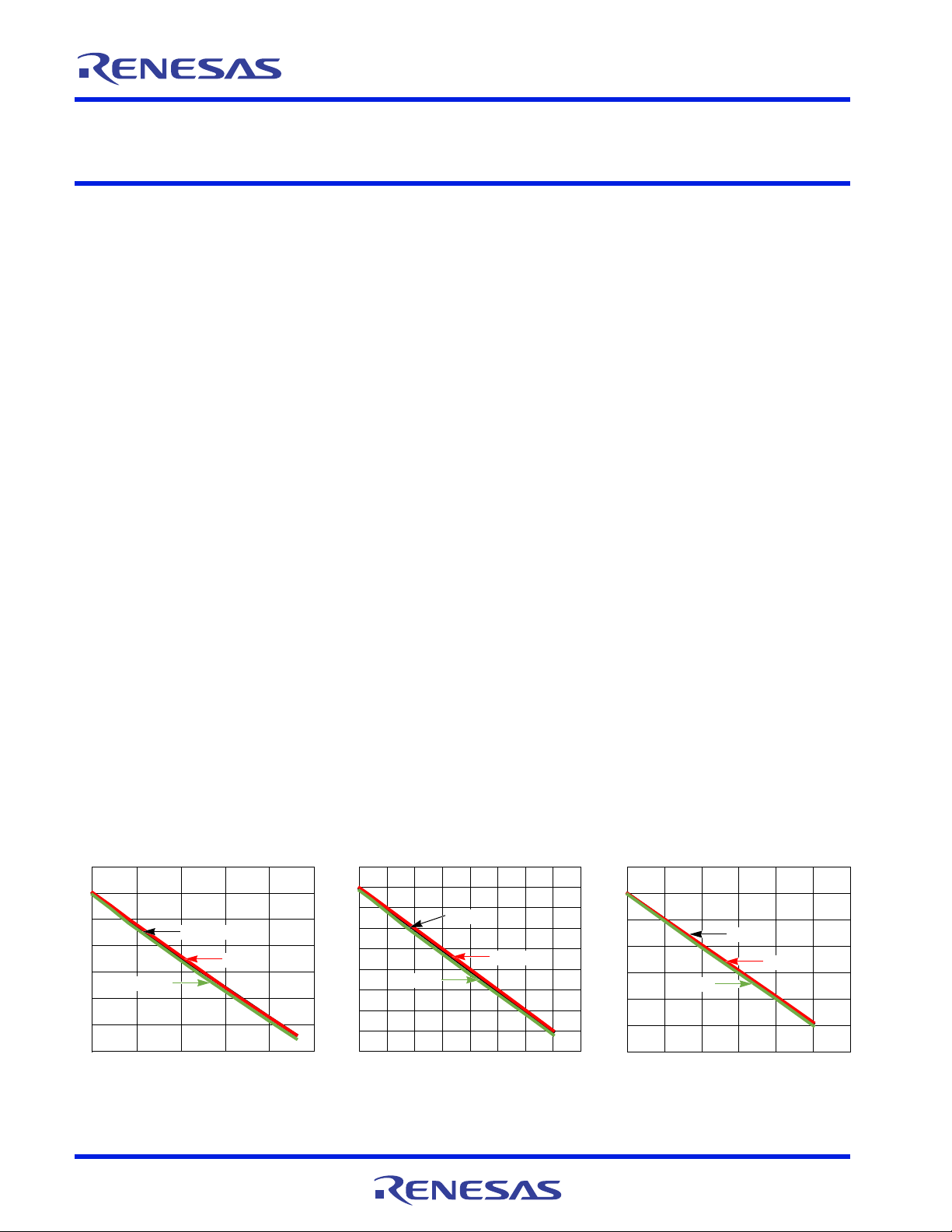
Figure 1. V
Line = 2.4mΩ
CORE
/VR A Load
FN8973 Rev.0.00 Page 1 of 74
Oct 6, 2017
Figure 2. VGT/VR B Load Line = 2mΩ
Figure 3. VSA/VR C Load Line = 10.3mΩ

ISL95859C
Contents
1. Overview. . . . . . . . . . . . . . . . . . . . . . . . . . . . . . . . . . . . . . . . . . . . . . . . . . . . . . . . . . . . . . . . . . . . . 4
1.1 Block Diagram . . . . . . . . . . . . . . . . . . . . . . . . . . . . . . . . . . . . . . . . . . . . . . . . . . . . . . . . . . . . . . 4
1.2 Simplified Application Circuits . . . . . . . . . . . . . . . . . . . . . . . . . . . . . . . . . . . . . . . . . . . . . . . . . . 5
1.3 Ordering Information . . . . . . . . . . . . . . . . . . . . . . . . . . . . . . . . . . . . . . . . . . . . . . . . . . . . . . . . . 7
1.4 Pin Configuration . . . . . . . . . . . . . . . . . . . . . . . . . . . . . . . . . . . . . . . . . . . . . . . . . . . . . . . . . . . . 7
1.5 Pin Descriptions . . . . . . . . . . . . . . . . . . . . . . . . . . . . . . . . . . . . . . . . . . . . . . . . . . . . . . . . . . . . . 8
2. Specifications. . . . . . . . . . . . . . . . . . . . . . . . . . . . . . . . . . . . . . . . . . . . . . . . . . . . . . . . . . . . . . . . 10
2.1 Absolute Maximum Ratings . . . . . . . . . . . . . . . . . . . . . . . . . . . . . . . . . . . . . . . . . . . . . . . . . . . 10
2.2 Thermal Information. . . . . . . . . . . . . . . . . . . . . . . . . . . . . . . . . . . . . . . . . . . . . . . . . . . . . . . . . 10
2.3 Recommended Operating Conditions . . . . . . . . . . . . . . . . . . . . . . . . . . . . . . . . . . . . . . . . . . . 10
2.4 Electrical Specifications . . . . . . . . . . . . . . . . . . . . . . . . . . . . . . . . . . . . . . . . . . . . . . . . . . . . . . 11
3. Typical Performance Curves for VR A . . . . . . . . . . . . . . . . . . . . . . . . . . . . . . . . . . . . . . . . . . . . 14
4. Typical Performance Curves for VR B . . . . . . . . . . . . . . . . . . . . . . . . . . . . . . . . . . . . . . . . . . . . 17
5. Typical Performance Curves for VR C . . . . . . . . . . . . . . . . . . . . . . . . . . . . . . . . . . . . . . . . . . . . 20
CONFIDENTIAL
6. Theory of Operation. . . . . . . . . . . . . . . . . . . . . . . . . . . . . . . . . . . . . . . . . . . . . . . . . . . . . . . . . . . 23
6.1 R3 Modulator . . . . . . . . . . . . . . . . . . . . . . . . . . . . . . . . . . . . . . . . . . . . . . . . . . . . . . . . . . . . . . 23
6.2 Multiphase Power Conversion . . . . . . . . . . . . . . . . . . . . . . . . . . . . . . . . . . . . . . . . . . . . . . . . . 23
6.3 Diode Emulation and Period Stretching . . . . . . . . . . . . . . . . . . . . . . . . . . . . . . . . . . . . . . . . . . 29
6.4 Adaptive Body Diode Conduction Time Reduction . . . . . . . . . . . . . . . . . . . . . . . . . . . . . . . . . 30
6.5 Modes of Operation . . . . . . . . . . . . . . . . . . . . . . . . . . . . . . . . . . . . . . . . . . . . . . . . . . . . . . . . . 30
6.6 Programming Resistors . . . . . . . . . . . . . . . . . . . . . . . . . . . . . . . . . . . . . . . . . . . . . . . . . . . . . . 32
6.7 PSYS System Power Monitoring . . . . . . . . . . . . . . . . . . . . . . . . . . . . . . . . . . . . . . . . . . . . . . . 33
7. General Design Guide . . . . . . . . . . . . . . . . . . . . . . . . . . . . . . . . . . . . . . . . . . . . . . . . . . . . . . . . . 34
7.1 Power Stages. . . . . . . . . . . . . . . . . . . . . . . . . . . . . . . . . . . . . . . . . . . . . . . . . . . . . . . . . . . . . . 34
7.2 Output Filter Design . . . . . . . . . . . . . . . . . . . . . . . . . . . . . . . . . . . . . . . . . . . . . . . . . . . . . . . . . 36
7.3 Input Capacitor Selection. . . . . . . . . . . . . . . . . . . . . . . . . . . . . . . . . . . . . . . . . . . . . . . . . . . . . 37
7.4 Inductor Current Sensing and Balancing . . . . . . . . . . . . . . . . . . . . . . . . . . . . . . . . . . . . . . . . . 38
7.5 Inductor DCR Current-Sensing Network . . . . . . . . . . . . . . . . . . . . . . . . . . . . . . . . . . . . . . . . . 38
7.6 Current Sense Circuit Adjustments . . . . . . . . . . . . . . . . . . . . . . . . . . . . . . . . . . . . . . . . . . . . . 49
7.7 Voltage Regulation. . . . . . . . . . . . . . . . . . . . . . . . . . . . . . . . . . . . . . . . . . . . . . . . . . . . . . . . . . 53
8. Fault Protection . . . . . . . . . . . . . . . . . . . . . . . . . . . . . . . . . . . . . . . . . . . . . . . . . . . . . . . . . . . . . . 65
8.1 VR_HOT#/ALERT# Behavior . . . . . . . . . . . . . . . . . . . . . . . . . . . . . . . . . . . . . . . . . . . . . . . . . 65
FN8973 Rev.0.00 Page 2 of 74
Oct 6, 2017

ISL95859C
9. Serial VID (SVID) Supported Data and Configuration Registers . . . . . . . . . . . . . . . . . . . . . . . 67
10. Layout Guidelines . . . . . . . . . . . . . . . . . . . . . . . . . . . . . . . . . . . . . . . . . . . . . . . . . . . . . . . . . . . . 69
11. Revision History. . . . . . . . . . . . . . . . . . . . . . . . . . . . . . . . . . . . . . . . . . . . . . . . . . . . . . . . . . . . . . 72
12. Package Outline Drawing . . . . . . . . . . . . . . . . . . . . . . . . . . . . . . . . . . . . . . . . . . . . . . . . . . . . . . 73
13. About Intersil . . . . . . . . . . . . . . . . . . . . . . . . . . . . . . . . . . . . . . . . . . . . . . . . . . . . . . . . . . . . . . . . 74
CONFIDENTIAL
FN8973 Rev.0.00 Page 3 of 74
Oct 6, 2017
ISL95859C 1. Overview
- V
DROOP
+
FROM
CPU
COMP_A
PWM_A
VR A
R3
TM
MODULATOR
RTN_A
DIGITAL
BLOCK
SVID
START-UP
PROTECTION
TALRT
VTT
VIN
VRHOT#
NTC_A
VCC
FB_A
AGND
SCLK
SDA
ALRT#
PROG1
PSYS
VR_READY
IMON_A
VR_ENABLE
FROM
CPU
+5V
TO CPU
TO CPU
FROM
CHARGER
IMON AND DROOP
CIRCUITRY
OCP
DROOP
ERROR
AMPLIFIER
ISUMP_A
ISUMN_A
FCCM_A
- V
DROOP
+
FROM
CPU
COMP_B
PWM1_B
VR B
R3
TM
MODULATOR
RTN_B
DIGITAL
BLOCK
SVID
START-UP
PROTECTION
ISUMP_B
ISUMN_B
FB_B
PROG2
IMON_B
OCP
DROOP
ERROR
AMPLIFIER
PWM2_B
FCCM_B
ISEN2_B
ISEN1_B
VIN
- V
DROOP
+
FROM
CPU
COMP_C
VR C
R3
TM
MODULATOR
RTN_C
DIGITAL
BLOCK
SVID
START-UP
PROTECTION
ISUMP_C
ISUMN_C
FB_C
IMON_C
OCP
DROOP
ERROR
AMPLIFIER
PWM_C
FCCM_C
CURRENT
SENSE
VIN
CURRENT
SENSE
AND
BALANCE
CURRENT
SENSE
AND
BALANCE
TALRT
NTC_B
IC THERMAL
MONITOR
IC THERMAL
MONITOR
IMON AND DROOP
CIRCUITRY
DIFF REMOTE
SENSING
DIFF REMOTE
SENSING
IMON AND DROOP
CIRCUITRY
DIFF REMOTE
SENSING
1. Overview
1.1 Block Diagram
CONFIDENTIAL
FN8973 Rev.0.00 Page 4 of 74
Figure 4. Block Diagram
Oct 6, 2017
VR_ ENABLE
VR_READY
VCC
SENSE_CPU
VR_ ENABLE
VR_READY
SDA
SDA
ALERT #
ALERT #
SCLK
SCLK
GND
VCC
VR_HOT#
VR_HOT#
V+5
ISL95859C
PSYS
VSS
SENSE_CPU
VCC
SENSE_SA
VSS
SENSE_SA
SA
V
CORE
NTC_B
FCCM_B
PWM_C
FCCM_C
ISUMP_C
ISUMN_C
COMP_C
FB_C
RTN_ C
PSYS
VIN
VIN
PROG1
PROG2
PWM1_ B
UGATE
LGATE
PHASE
BOOT
PWM
FCCM
GND
ISL95808
VCC
VIN
°C
IMON_C
IMON_ A
FB_A
RTN_ A
VCC
SENSE_GT
GT
V
CORE
VSS
SENSE_GT
ISUMP_B
ISUMN_B
ISEN1_B
ISEN2_B
VIN
PWM2_B
VIN
UGATE
LGATE
PHASE
BOOT
PWM
FCCM
GND
ISL95808
VCC
V+5
UGATE
LGATE
PHASE
BOOT
PWM
FCCM
GND
ISL95808
VCC
COMP _B
FB_B
RTN_ B
°C
°C
V+5
IMON_B
NTC_ A
°C
SA
V
CORE
PWM_A
FCCM_ A
ISUMP_A
ISUM N_ A
COMP_ A
UGATE
LGATE
PHASE
BOOT
PWM
FCCM
GND
ISL95808
VCC
VIN
V+5
°C
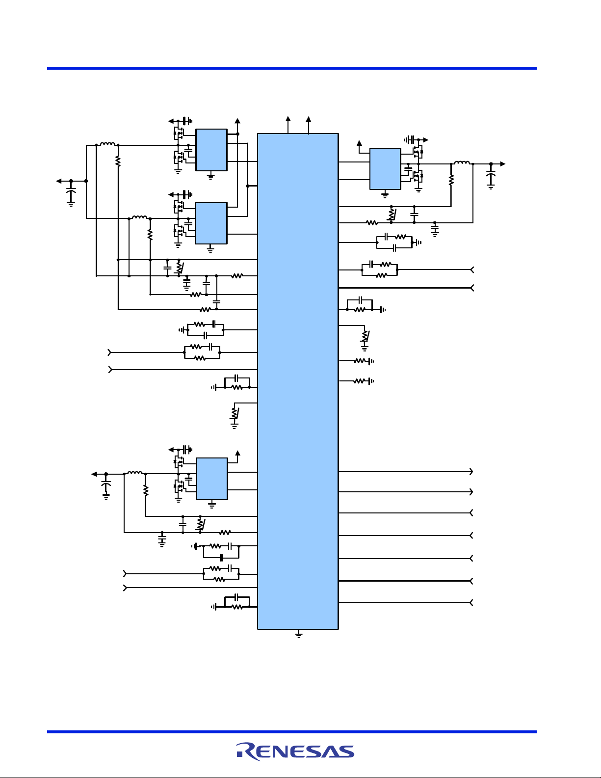
ISL95859C 1. Overview
1.2 Simplified Application Circuits
CONFIDENTIAL
Figure 5. Typical ISL95859C Application Circuit Using Inductor DCR Current Sensing
FN8973 Rev.0.00 Page 5 of 74
Oct 6, 2017
ISL95859C 1. Overview
VR_ ENABLE
VR_READY
VCC
SENSE_CPU
VR_ENABLE
VR_READY
SDA
SDA
ALERT #
ALERT #
SCLK
SCLK
GND
VCC
VR_HOT#
VR_HOT#
V+5
ISL95859 C
CPU
V
CORE
PSYS
VSS
SENSE_CPU
NTC _B
FCCM_B
PSYS
VIN
VIN
PROG1
PROG2
PWM1_B
IMON_ A
FB_A
RTN_A
VCC
SENSE_GT
GT
V
CORE
VSS
SENSE_GT
ISUMP_B
ISUMN_B
ISEN1_B
ISEN2_B
VIN
PWM2_B
VIN
UGATE
LGATE
PHASE
BOOT
PWM
FCCM
GND
ISL 9580 8
VCC
V+5
UGATE
LGATE
PHASE
BOOT
PWM
FCCM
GND
ISL 9580 8
VCC
COMP_B
FB_B
RTN _B
°C
IMON_ B
NTC_A
°C
PWM_A
FCCM_A
ISUMP_A
ISUMN_A
UGATE
LGATE
PHASE
BOOT
PWM
FCCM
GND
ISL 95808
VCC
VIN
V+5
VCC
SENSE_SA
VSS
SENSE_SA
SA
V
CORE
PWM_C
FCCM_C
ISUMP_C
ISUMN_C
COMP_ C
FB_C
RTN_C
UGATE
LGATE
PHASE
BOOT
PWM
FCCM
GND
ISL 95808
VCC
VIN
IMON_ C
V+5
COMP_ A
CONFIDENTIAL
Figure 6. Typical ISL95859C Application Circuit Using Resistor Sensing
FN8973 Rev.0.00 Page 6 of 74
Oct 6, 2017
ISL95859C 1. Overview
40 39 38 37 36 35 34 33 32 31
29
30
27
28
25
26
23
24
21
22
11 12 13 14 15 16 17 18 19
2
1
4
3
6
5
8
7
10
9
GND
(BOTTOM PAD)
NTC_B
COMP_B
FB_B
ISUMP_B
RTN_C
FB_C
COMP_C
ISUMP_C
ISUMN_C
SDA
SCLK
ALERT#
PROG2
PROG1
ISUMN_B
20
VR_HOT#
RTN_B
VR_ENABLE
FCCM_B
PWM1_B
PWM2_B
IMON_A
COMP_A
FB_A
RTN_A
ISUMP_A
NTC_A
ISEN 1_B
VR_READY
FCCM_A
ISUMN_A
FCCM_C
PWM_ C
PWM_ A
PSYS
IMON_B
IMON_C
VCC
ISEN 2_B
VIN
1.3 Ordering Information
Part Number
(Notes 1
ISL95859CHRTZ 95859C HRTZ -10 to +100 40 Ld 5x5 TQFN L40.5x5
ISL95859CIRTZ 95859C IRTZ -40 to +100 40 Ld 5x5 TQFN L40.5x5
Notes:
1. Add “-T” for 6k unit tape and reel options. Refer to TB347
2. These Intersil Pb-free plastic packaged products employ special Pb-free material sets, molding compounds/die attach materials
and 100% matte tin plate plus anneal (e3 termination finish, which is RoHS compliant and compatible with both SnPb and Pbfree soldering operations). Intersil
Pb-free products are MSL classified at Pb-free peak reflow temperatures that meet or exceed the Pb-free requirements of
IPC/JEDEC J STD-020.
3. For more information on MSL, refer to TB363
, 2, 3)Part Marking
.
Temp Range
(°C)
for details on reel specifications.
Package
(RoHS Compliant)
Pkg.
Dwg. #
1.4 Pin Configuration
ISL95859C
(40 LD TQFN)
Top View
CONFIDENTIAL
FN8973 Rev.0.00 Page 7 of 74
Oct 6, 2017

ISL95859C 1. Overview
1.5 Pin Descriptions
Pin Number Pin Name Description
BOTTOM PAD GND Signal common to the IC. Unless otherwise stated, all signals are referenced to the GND pad. It is also
the primary thermal conduction pad for heat removal. Connect this ground pad to the ground plane or
planes through a low impedance path. Best performance is obtained with an uninterrupted ground plane
under the ISL95859C and all associated components, signal sources, signal paths and extending from
the controller to the load. Do not attempt to isolate signal and power grounds.
1 PSYS Analog input from the platform battery charger that is proportional to real-time, total system power
dissipation. Information is to be digitized and stored by the controller to be read by the CPU from SVID.
2 IMON_B Regulator B current monitor. The IMON_B pin sources a current proportional to the regulator output
3 NTC_B Thermistor input from VR B to the temperature monitor circuit of the IC controlling the VR_HOT# output.
4 COMP_B Output of the transconductance error amplifier for VR B regulation and stability. Connect to ground
5 FB_B Output voltage feedback sensing input for regulation of Regulator B. Connect to the remote positive
6 RTN_B Ground return for differential remote output voltage sensing. Connect to the remote negative sense point
CONFIDENTIAL
7 ISUMP_B VR B droop current sensing inputs.
8ISUMN_B
9 ISEN1_B Individual current sensing for VR B Phase 1. This signal monitors and corrects for phase current
10 ISEN2_B Individual current sensing for VR B Phase 2. When ISEN2_B is pulled to VDD (+5V), the controller will
11 FCCM_B Driver control signal for Regulator B. When FCCM_B is high, continuous conduction mode is forced.
12 PWM1_B Regulator B, Channel 1 PWM output. See “
13 PWM2_B Regulator B, Channel 2 PWM output. See “
14 IMON_A Regulator A current monitor. The IMON_A pin sources a current proportional to the regulator output
15 NTC_A Thermistor input from VR A to the temperature monitor circuit of the IC controlling the VR_HOT# output.
16 COMP_A Output of the transconductance error amplifier for VR A regulation and stability. Connect to ground
17 FB_A Output voltage feedback sensing input for regulation of Regulator A. Connect to the remote positive
18 RTN_A Ground return for differential remote output voltage sensing. Connect to the remote negative sense point
current. A resistor connected from this pin to ground will set a voltage that is proportional to the load
current. This voltage is sampled internally to produce a digital IMON signal that is read through the serial
communication bus.
Connect this pin to a resistor network with a thermistor (NTC) to GND. A current is sourced from the pin
and generates a voltage, which is monitored versus an internal threshold to determine when the VR is too
hot.
through a type-II network to compensate the control loop.
sense point on the CPU through a resistor. The resistor value is used to scale droop for VR B.
on the CPU through a resistor.
Connecting ISUMN_B to VCC disables VR B.
imbalance. In 1-phase configurations, connect ISEN1_B to VCC or leave it open.
disable VR Phase 2. This signal is used to monitor and correct for phase current imbalance.
When FCCM_B is low, diode emulation is allowed. FCCM_B is high impedance and interfaces with the
ISL95808 or similar driver when entering a PS4 state.
Driver Selection” on page 35 for more information on
interfacing with the ISL95808 driver or compatible power stages.
Driver Selection” on page 35 for more information on
interfacing with the ISL95808 driver or compatible power stages.
current. A resistor connected from this pin to ground will set a voltage that is proportional to the load
current. This voltage is sampled internally to produce a digital IMON_A signal that is read through the
serial communication bus.
Connect this pin to a resistor network with a thermistor (NTC) to GND. A current is sourced from the pin
and generates a voltage, which is monitored versus an internal threshold to determine when the VR is too
hot.
through a type-II network to compensate the control loop.
sense point on the CPU through a resistor. The resistor value is used to scale droop for VR A.
on the CPU through a resistor.
FN8973 Rev.0.00 Page 8 of 74
Oct 6, 2017

ISL95859C 1. Overview
Pin Number Pin Name Description
19 ISUMP_A VR A droop current sensing inputs.
20 ISUMN_A
21 FCCM_A Driver control signal for Regulator A. When FCCM_A is high, Continuous Conduction Mode (CCM) is
22 PWM_A Regulator A, PWM output. See “
23 IMON_C Regulator C current monitor. The IMON_C pin sources a current proportional to the regulator output
24 COMP_C Output of the transconductance error amplifier for VR C regulation and stability. Connect to ground
25 FB_C Output voltage feedback sensing input for regulation of Regulator C. Connect to the remote positive
26 RTN_C Ground return for differential remote output voltage sensing. Connect to the remote negative sense point
27 ISUMP_C VR C droop current sensing inputs.
28 ISUMN_C
29 FCCM_C Driver control signal for Regulator C. When FCCM_C is high, Continuous Conduction Mode (CCM) is
CONFIDENTIAL
30 PWM_C Regulator C, PWM Output. See “
31 PROG2 Place a resistor from this pin to GND. The resistor value is selected based on programming options
32 PROG1 Place a resistor from this pin to GND. The resistor value is selected based on programming options
33 VIN Input supply voltage used for input voltage feed-forward.
34 VCC +5V bias supply input for the controller. Bypass to ground with a high quality 0.1µF ceramic capacitor.
35 SDA Communication bus between the CPU and the VRs.
36 ALERT#
37 SCLK
38 VR_HOT# Open-drain thermal overload output indicator. Considered part of the communication bus with the CPU.
39 VR_READY Power-good open-drain output indicating when controller is able to supply regulated voltage on all
40 VR_ENABLE Controller enable input. A high level logic signal on this pin enables the controller.
Connecting ISUMN_A to VCC disables VR A.
forced. When FCCM_A is low, diode emulation is allowed. FCCM_A is high impedance and interfaces
with the ISL95808 or similar driver when entering a PS4 state.
Driver Selection” on page 35 for more information on interfacing with the
ISL95808 driver or compatible power stages.
current. A resistor connected from this pin to ground will set a voltage that is proportional to the load
current. This voltage is sampled internally to produce a digital IMON signal that is read through the serial
communication bus.
through a type-II network to compensate the control loop.
sense point on the CPU through a resistor. The resistor value is used to scale droop for VR C.
on the CPU through a resistor.
Connecting ISUMN_C to VCC disables VR C.
forced. When FCCM_C is low, diode emulation is allowed. FCCM_C is high impedance and interfaces
with the ISL95808 or similar driver when entering a PS4 state.
Driver Selection” on page 35 for more information on interfacing with the
ISL95808 driver or compatible power stages.
defined in the controller option tables.
defined in the controller option tables.
This pin establishes the voltage reference for all PWM and FCCM driver interface outputs. To ensure
proper operation of drivers, especially during power-up and power-down sequencing, it is essential that
this pin be powered with the same +5V power supply as the VCC or VCCP pins of the Intersil gate
drivers.
outputs. Pull up externally with a 680Ω resistor to VCC or 1.9kΩ to 3.3V
FN8973 Rev.0.00 Page 9 of 74
Oct 6, 2017
ISL95859C 2. Specifications
2. Specifications
2.1 Absolute Maximum Ratings
Parameter Minimum Maximum Unit
Supply Voltage, V
Battery Voltage, V
All Other Pins -0.3 V
Open-Drain Outputs, VR_READY, VR_HOT#, ALERT# -0.3 +6.5 V
Human Body Model (Tested per JESD22-A114E) 2 kV
Charged Device Model (Tested per JESD22-C101A) 1 kV
Latch-Up (Tested per JESD78B; Class 2, Level A) 100 mA
CAUTION: Do not operate at or near the maximum ratings listed for extended periods of time. Exposure to such conditions may
adversely impact product reliability and result in failures not covered by warranty.
CC
IN
ESD Rating Value Unit
2.2 Thermal Information
Thermal Resistance (Typical)
40 Ld TQFN Package (Notes 4, 5)30 1.5
Notes:
4.
is measured in free air with the component mounted on a high-effective thermal conductivity test board with “direct attach”
JA
CONFIDENTIAL
features. Refer to TB379
5. For
, the “case temp” location is the center of the exposed metal pad on the package underside.
JC
.
(°C/W) JC (°C/W)
JA
-0.3 +6.5 V
+28 V
+ 0.3 V
CC
Parameter Minimum Maximum Unit
Maximum Junction Temperature +150 °C
Maximum Storage Temperature Range -65 +150 °C
Maximum Junction Temperature (Plastic Package) +150 °C
Storage Temperature Range -65 +150 °C
Pb-Free Reflow Profile Refer to TB493
2.3 Recommended Operating Conditions
Parameter Minimum Maximum Unit
Supply Voltage, V
Input Voltage, VIN +4.5 25 V
Ambient Temperature
HRTZ -10 +100 °C
IRTZ -40 +100 °C
Junction Temperature
HRTZ -10 +125 °C
IRTZ -40 +125 °C
CC
+5V ±5% V
FN8973 Rev.0.00 Page 10 of 74
Oct 6, 2017
ISL95859C 2. Specifications
2.4 Electrical Specifications
V
= 5V, VIN = 15V, fSW = 583kHz, unless otherwise noted. Boldface limits apply across the operating temperature range
CC
T
= -40°C to +100°C for industrial (IRTZ) and TA = -10°C to +100°C for high temperature commercial (HRTZ).
A
Min
Symbol Parameter Test Conditions
Input Power Supply
I
VCC
I
R
Power-on-Reset Thresholds
VCCPOR
VCCPOR
VINPOR
VINPOR
System and References
HRTZ System Accuracy VID = 0.75V to 1.52V -0.5 0.5 %
IRTZ VID = 0.75V to 1.52V -0.8 0.8 %
HRTZ SA Internal V
IRTZ 1.05 V
HRTZ IA, GT, GTUS Internal V
IRTZ 0V
V
OUT(max)
V
OUT(min)
Switching Frequency
f
SW_450k
f
SW_583k
f
SW_750k
Amplifiers
HRTZ Current-sense Amplifier Input
IRTZ -0.3 0.3 mV
A
GBW Error Amplifier
+5V Supply Current VR_ENABLE = 1V (PWMs are not
VIN Supply Current VR_ENABLE = 0V 1 µA
VIN
VIN Input Resistance VR_ENABLE = 1V 700 kΩ
VIN
Power-On Reset
rVCC
Threshold
f
Power-On Reset
rVIN
Threshold
f
CONFIDENTIAL
BOOT
Maximum Programmed
Output Voltage
Minimum Programmed
Output Voltage
450kHz Configuration Set by R_PROG1 and R_PROG2 415 500 kHz
583kHz Configuration 540 630 kHz
750kHz Configuration 685 795 kHz
Offset
Error Amplifier DC Gain
v0
(Note 7
)
Gain-Bandwidth Product
(Note 7
)
switching)
VR_ENABLE = 0V 1 µA
PS4 state for all VRs and input power
domain
VCC rising 4.40 4.50 V
VCC falling 4.00 4.15 V
VIN rising 4.00 4.35 V
VIN falling 2.90 3.40 V
VID = 0.5V to 0.745V -7 7 mV
VID = 0.25V to 0.495V -10 10 mV
VID = 0.5V to 0.745V -9 9 mV
VID = 0.25V to 0.495V -12 12 mV
BOOT
VI D = [11111111] 1. 52 V
VID = [00000001] 0.25 V
= 0A -0.2 0.2 mV
I
FB
C
= 20pF 30 MHz
L
(Note 6
)Typ
16 18 mA
80 140 µA
1.05 V
0V
38 dB
Max
(Note 6)Unit
FN8973 Rev.0.00 Page 11 of 74
Oct 6, 2017
ISL95859C 2. Specifications
= 5V, VIN = 15V, fSW = 583kHz, unless otherwise noted. Boldface limits apply across the operating temperature range
V
CC
T
= -40°C to +100°C for industrial (IRTZ) and TA = -10°C to +100°C for high temperature commercial (HRTZ).
A
Symbol Parameter Test Conditions
ISEN
Imbalance Voltage Maximum of ISENs - minimum of
ISENs
Input Bias Current 20 nA
Power-Good and Protection Monitors
V
I
PWM and FCCM
V
V
t
PS4EXIT
Protection
OV
Logic Thresholds
V
V
V
Thermal Monitor
VR_READY Low Voltage I
OL
VR_READY Leakage Current VR_READY = 3.3V 1 µA
OH
ALERT# Low Voltage
(Note 7
VR_HOT# Low Voltage
(Note 7
ALERT# Leakage Current 1 µA
VR_HOT# Leakage Current 1 µA
PWM Output Low Sinking 5mA 0.6 0.9 V
0L
FCCM Output Low Sinking 4mA 0.6 0.9 V
PWM Output High (Note 7) Sourcing 5mA 3.5 4.2 V
0H
FCCM Output High (Note 7
CONFIDENTIAL
PWM Tri-State Voltage 2.5 V
FCCM Mid-State Voltage 2.5 V
PWM Tri-State and FCCM
High Impedance Leakage
PS4 Exit Latency VCC = 5V 50 100 µs
Overvoltage Threshold ISUMN rising above setpoint for >1µs 240 360 mV
H
Overcurrent Threshold
(ISUMN Pin Current)
VR_ENABLE Input Low 0.3 V
IL
VR_ENABLE Input High HRTZ 0.7 V
IH
IH
NTC Source Current NTC = 1.3V 9.5 10 10.5 µA
VR_HOT# Trip Voltage Falling 0.187 0.198 0.209 V
VR_HOT# Reset Voltage Rising 0.209 0.220 0.231 V
VR_HOT# Hysteresis 20 mV
Thermal Alert Trip Voltage Falling 0.203 0.214 0.225 V
Thermal Alert Reset Voltage Rising 0.225 0.236 0.247 V
Thermal Alert Hysteresis 20 mV
VR_READY
)
)
) Sourcing 4mA 3.3 3.6 V
PWM and FCCM = 2.5V -1 1 µA
2-phase configuration PS0 state or
1-phase configuration covering all
power states
2-phase configuration with 1-phase
operation in PS1, PS2 and PS3 states
IRTZ 0.75 V
= 4mA 0.15 0.40 V
Min
(Note 6
)Typ
7 12 Ω
7 12 Ω
56 60 64 µA
27 30 33 µA
Max
(Note 6)Unit
1 mV
FN8973 Rev.0.00 Page 12 of 74
Oct 6, 2017
ISL95859C 2. Specifications
V
= 5V, VIN = 15V, fSW = 583kHz, unless otherwise noted. Boldface limits apply across the operating temperature range
CC
T
= -40°C to +100°C for industrial (IRTZ) and TA = -10°C to +100°C for high temperature commercial (HRTZ).
A
Symbol Parameter Test Conditions
Current Monitor
I
IMON
V
IMONrICCMAX
V
IMONf
Inputs
I
VR_ENABLE
Slew Rate (For VID Change)
Notes:
6. Parameters with MIN and/or MAX limits are 100% tested at +25°C, unless otherwise specified. Temperature limits established by
7. Limits established by characterization and are not production tested.
IMON Output Current ISUM- pin current = 40µA 9.7 10 10.3 µA
ISUM- pin current = 20µA 4.8 5 5.2 µA
ISUM- pin current = 4µA 0.875 1 1.125 µA
Alert Trip Voltage Rising 1.185 1.200 1.215 V
I
Alert Reset Voltage Falling 1.115 1.130 1.145 V
CCMAX
VR_ENABLE Leakage
Current
SCLK, SDA Leakage VR_ENABLE = 0V, SCLK and
CONFIDENTIAL
Fast Slew Rate 30 mV/µs
Slow Slew Rate 15 mV/µs
SVID
SVID CLK Maximum Speed
(Note 7
)
SVID CLK Minimum Speed
(Note 7
)
characterization and are not production tested.
VR_ENABLE = 0V -1 0µA
VR_ENABLE = 1V 3 5 µA
SDA = 0V and 1V
VR_ENABLE = 1V, SCLK and
SDA = 1V
VR_ENABLE = 1V, SCLK and
SDA = 0V, SCLK Leakage
VR_ENABLE = 1V, SCLK and
SDA = 0V, SDA Leakage
Min
(Note 6
)Typ
-1 1 µA
-5 1 µA
-42 µA
-24 µA
42 MHz
13 MHz
Max
(Note 6)Unit
FN8973 Rev.0.00 Page 13 of 74
Oct 6, 2017
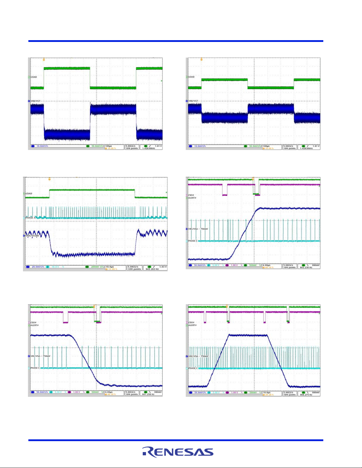
ISL95859C 3. Typical Performance Curves for VR A
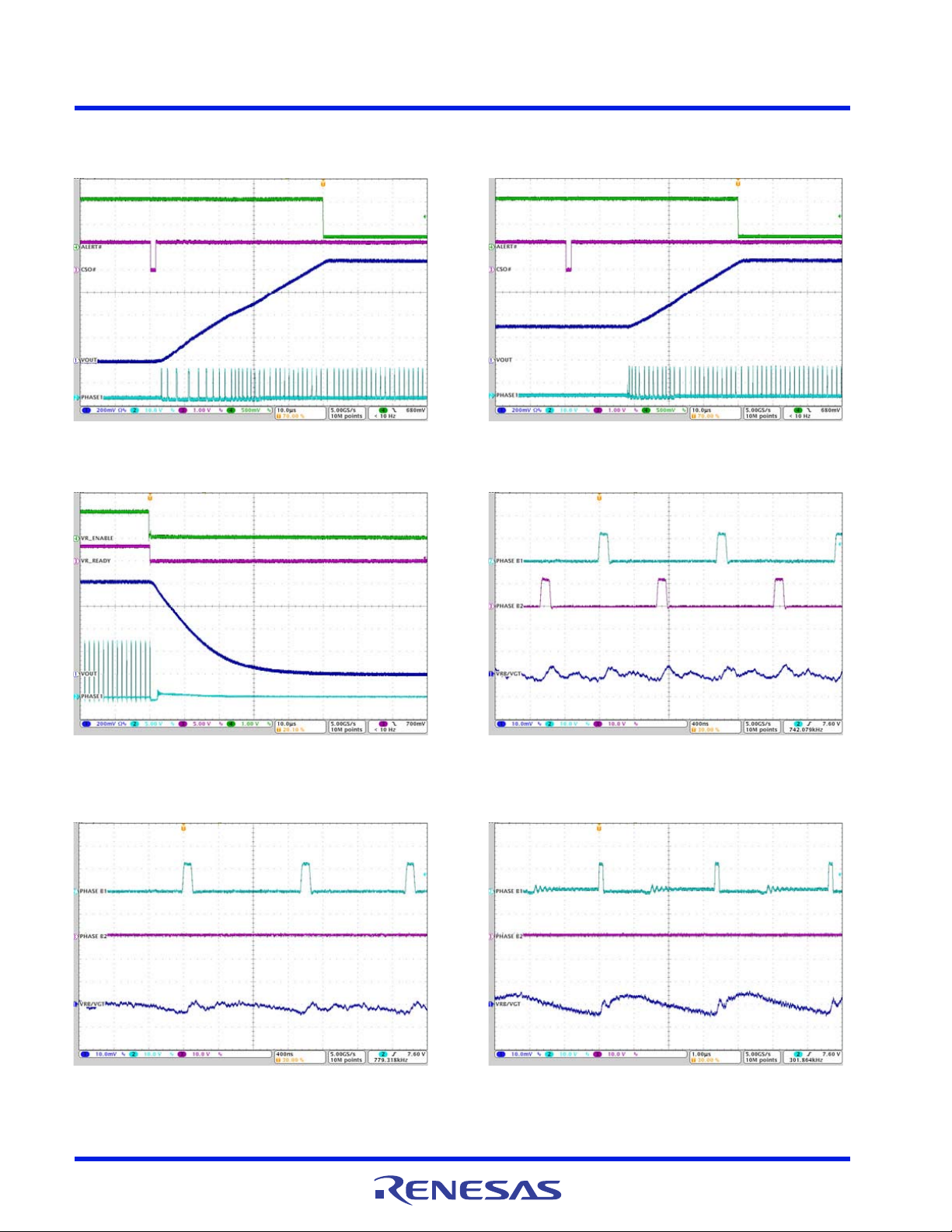
3. Typical Performance Curves for VR A
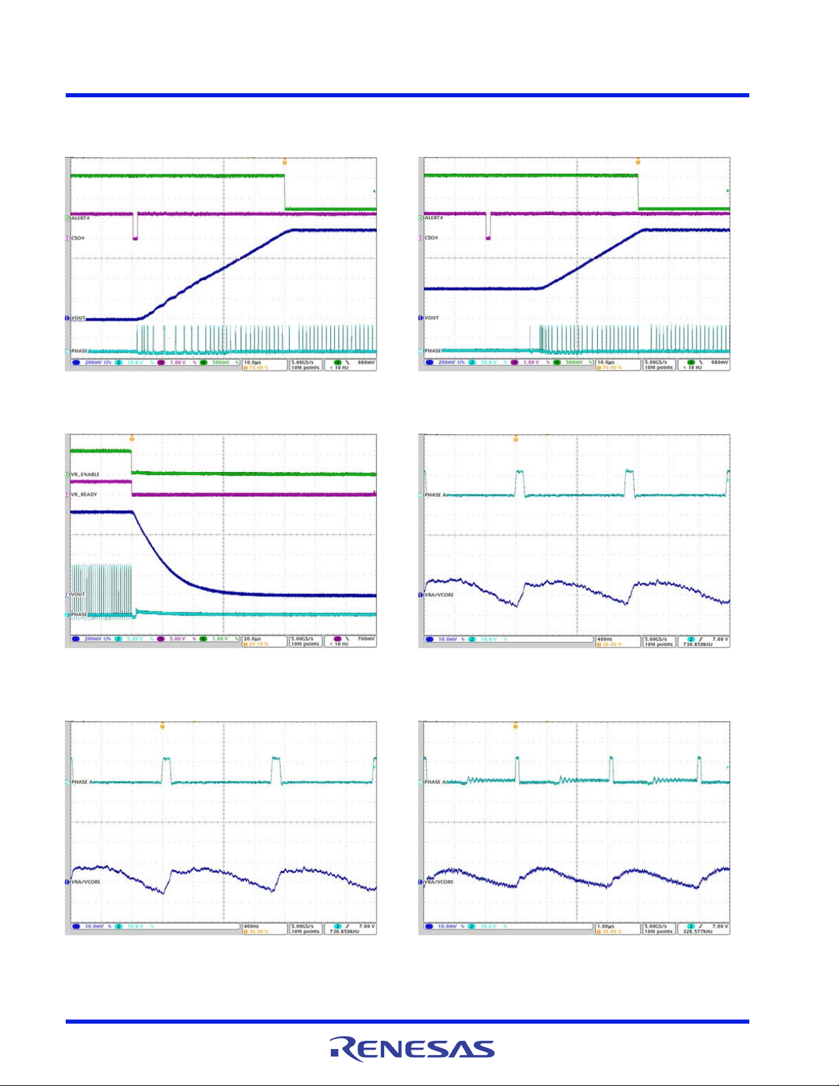
Figure 7. V
Figure 9. V
/VR A Soft-Start, SetVID_fast 0V to 0.9V,
CORE
I
O
=0A
Figure 8. V
/VR A Soft-Start with Precharged Output,
CORE
SetVID_fast 0.9V, I
= 0A
O
CONFIDENTIAL
/VR A Shutdown, IO= 23A, VID = 0.9V
CORE
Figure 10. V
/VR A PS0 Steady-State Phase and
CORE
Ripple, IO= 23A, VID = 0.9V
Figure 11. V
FN8973 Rev.0.00 Page 14 of 74
Oct 6, 2017
/VR A PS1 Steady-State Phase and
CORE
Ripple, IO= 23A, VID = 0.9V
Figure 12. V
/VR A PS2 Steady-State Phase and
CORE
Ripple, IO= 2A, VID = 0.9V
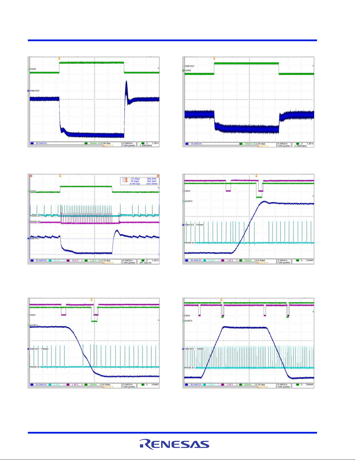
ISL95859C 3. Typical Performance Curves for VR A
Figure 13. V
CONFIDENTIAL
Figure 15. V
/VR A PS0 Load Step, IO = 4A to 29A,
CORE
VID = 0.9V, R_LL = 2.4mΩ
/VR A Load Step, IO = 1A IN PS2 to 26A
CORE
in PS0, VID = 0.9V, R_LL = 2.4mΩ
Figure 14. V
Figure 16. V
/VR A PS0 Load Step, IO = 18A to 28A,
CORE
VID = 0.9V, R_LL = 2.4mΩ
/VR A SetVID_fast, 0.6V to 0.9V, PS0,
CORE
IO= 7A, R_LL = 2.4mΩ
Figure 17. V
FN8973 Rev.0.00 Page 15 of 74
Oct 6, 2017
/VR A SetVID_fast, 0.9V to 0.6V, PS0,
CORE
IO= 7A, R_LL = 2.4mΩ
Figure 18. V
/VR A SetVID_slow, 0.6V to 0.9V to 0.6V,
CORE
PS0, IO= 7A, R_LL = 2.4mΩ
ISL95859C 3. Typical Performance Curves for VR A
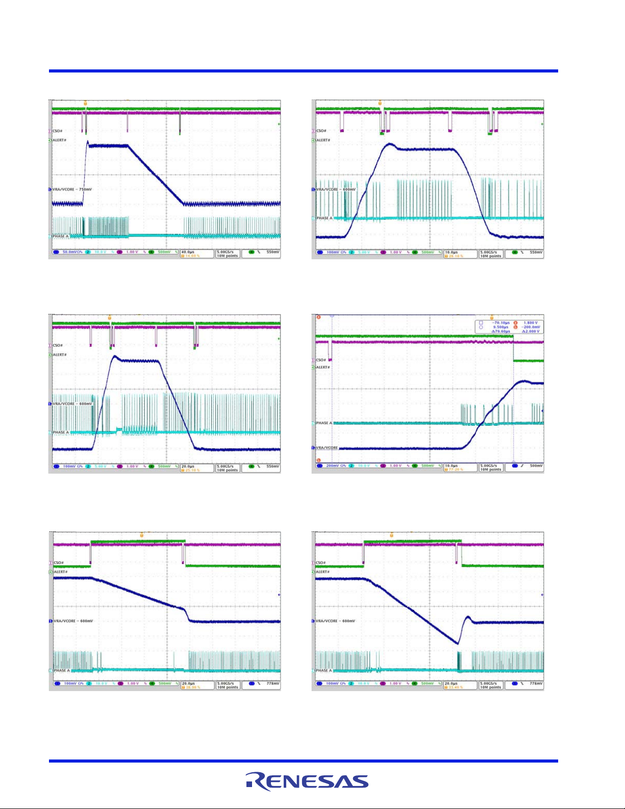
Figure 19. V
SetVID_decay, 0.9V to 0.7V, IO = 1.5A, R_LL = 2.4mΩ
/VR A SetVID_fast, 0.7V to 0.9V, PS0,
CORE
CONFIDENTIAL
Figure 21. V
SetVID_slow to 0.3V, PS2, I
/VR A SetVID_fast, 0.3V to 0.9V,
CORE
= 1A, R_LL = 2.4mΩ
O
Figure 20. V
Figure 22. V
/VR A SetVID_fast, 0.3V to 0.9V to 0.3V,
CORE
PS1, IO= 7A, R_LL = 2.4mΩ
/VR A PS4 EXIT, SetVID_fast 0.9V, PS0,
CORE
= 0A, R_LL = 2.4mΩ
I
O
Figure 23. V
Pre-Empted Downward by SetVID_fast 0.6V, IO = 2.1A,
FN8973 Rev.0.00 Page 16 of 74
Oct 6, 2017
/VR A SetVID_decay 0.9V to 0.3V,
CORE
R_LL = 2.4mΩ
Figure 24. V
Pre-Empted Upward by SetVID_fast 0.6V, IO = 4.4A,
/VR A SetVID_decay 0.9V to 0.3V,
CORE
R_LL = 2.4mΩ
ISL95859C 4. Typical Performance Curves for VR B
4. Typical Performance Curves for VR B
Figure 25. VGT/VR B Soft-Start, SetVID_fast 0V to 0.9V,
=0A
I
O
CONFIDENTIAL
Figure 27. VGT/VR B Shutdown, IO= 35A, VID = 0.9V
Figure 26. VGT/VR B Soft-Start with Precharged Output,
SetVID_fast 0.9V, IO = 0A
Figure 28. VGT/VR B PS0 Steady-State Phase and Ripple,
I
= 35A, VID = 0.9V
O
Figure 29. VGT/VR B PS1 Steady-State Phase and Ripple,
= 10A, VID = 0.9V
I
O
FN8973 Rev.0.00 Page 17 of 74
Oct 6, 2017
Figure 30. VGT/VR B PS2 Steady-State Phase and Ripple,
= 2A, VID = 0.9V
I
O
ISL95859C 4. Typical Performance Curves for VR B
Figure 31. VGT/VR B PS0 Load Step, IO = 11A to 57A,
VID = 0.9V, R_LL = 2.0mΩ
CONFIDENTIAL
Figure 33. VGT/VR B Load Step, I
PS0, VID = 0.9V, R_LL = 2.0mΩ
= 1A in PS2 to 47A in
O
Figure 32. IVGT/VR B PS0 Load Step, IO = 30A to 40A,
VID = 0.9V, R_LL = 2.0mΩ
Figure 34. VGT/VR B SetVID_fast, 0.6V to 0.9V, PS0,
= 11A, R_LL = 2.0mΩ
I
O
Figure 35. IVGT/VR B SetVID_fast, 0.9V to 0.6V, PS0,
= 11A, R_LL = 2.0mΩ
I
O
FN8973 Rev.0.00 Page 18 of 74
Oct 6, 2017
Figure 36. VGT/VR B SetVID_slow, 0.6V to 0.9V to 0.6V,
PS0, I
= 11A, R_LL = 2.0mΩ
O
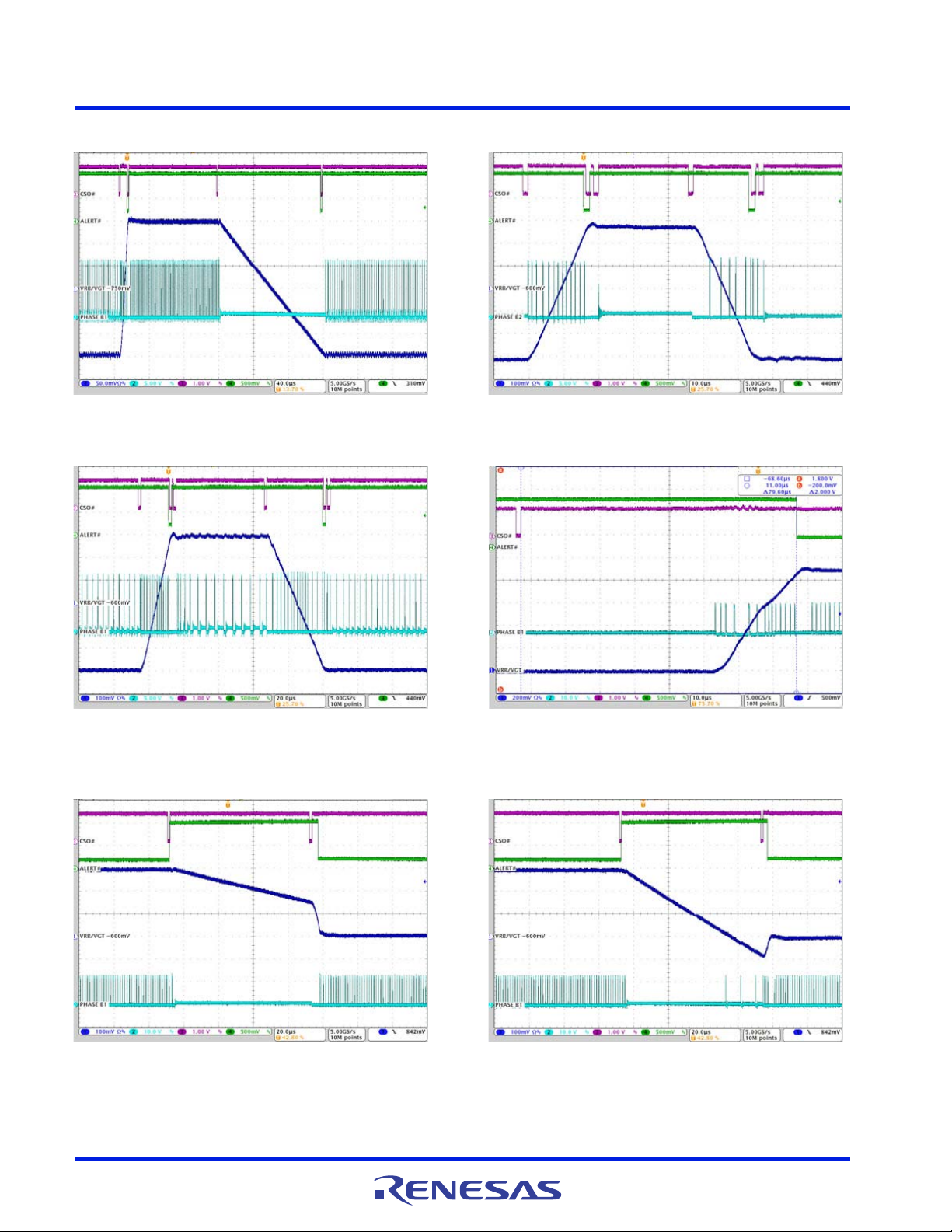
ISL95859C 4. Typical Performance Curves for VR B
Figure 37. VGT/VR B SetVID_fast, 0.6V to 0.9V, PS0,
SetVID_decay, 0.9V to 0.6V, IO = 2A, R_LL = 2.0mΩ
CONFIDENTIAL
Figure 39. VGT/VR B SetVID_fast, 0.3V to 0.9V,
SetVID_slow to 0.3V, PS2, I
= 1A, R_LL = 2.0mΩ
O
Figure 38. VGT/VR B SetVID_fast, 0.3V to 0.9V to 0.3V, PS1,
IO= 10A, R_LL = 2.0mΩ
Figure 40. VGT/VR B PS4 Exit, SetVID_fast 0.9V, PS0,
= 0A, R_LL = 2.0mΩ
I
O
Figure 41. VGT/VR B SetVID_decay 0.9V to 0.3V,
Pre-Empted Downward by SetVID_fast 0.6V, I
R_LL = 2.0mΩ
FN8973 Rev.0.00 Page 19 of 74
Oct 6, 2017
= 1.5A,
O
Figure 42. VGT/VR B SetVID_decay 0.9V to 0.3V,
Pre-Empted Upward by SetVID_fast 0.6V, I
R_LL = 2.0mΩ
= 4A,
O
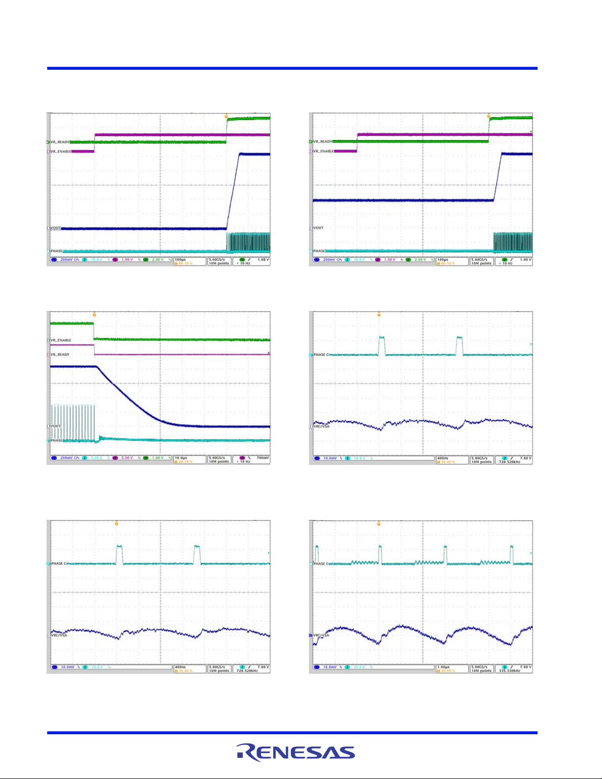
ISL95859C 5. Typical Performance Curves for VR C
5. Typical Performance Curves for VR C
Figure 43. VSA/VR C Soft-Start, 0V to V
=0A
I
O
BOOT
= 1.05V,
CONFIDENTIAL
Figure 45. VSA/VR C Shutdown, IO=5A, VID=0.9V
Figure 44. VSA/VR C Soft-Start with Precharged Output,
V
= 1.05V, IO = 0A
BOOT
Figure 46. VSA/VR C PS0 Steady-State Phase and Ripple,
I
= 5A, VID = 0.9V
O
Figure 47. VSA/VR C PS1 Steady-State Phase and Ripple,
= 5A, VID = 0.9V
I
O
FN8973 Rev.0.00 Page 20 of 74
Oct 6, 2017
Figure 48. VSA/VR C PS0 Steady-State Phase and Ripple,
IO= 1A, VID = 0.9V
ISL95859C 5. Typical Performance Curves for VR C
Figure 49. VSA/VR C PS0 Load Step, IO = 2A to 5A,
VID = 0.9V, R_LL = 10.3mΩ
CONFIDENTIAL
Figure 51. VSA/VR C Load Step, I
PS0, VID = 0.9V, R_LL = 10.3mΩ
= 1A in PS2 to 5A in
O
Figure 50. VSA/VR C PS0 Load Step, IO = 2A to 3A,
VID = 0.9V, R_LL = 10.3mΩ
Figure 52. VSA/VR C SetVID_fast, 0.6V to 0.9V, PS0,
IO= 3A, R_LL = 10.3mΩ
Figure 53. VSA/VR C SetVID_fast, 0.9V to 0.6V, PS0,
I
= 3A, R_LL = 10.3mΩ
O
FN8973 Rev.0.00 Page 21 of 74
Oct 6, 2017
Figure 54. VSA/VR C SetVID_slow, 0.6V to 0.9V to 0.6V,
PS0, I
= 3A, R_LL = 10.3mΩ
O
ISL95859C 5. Typical Performance Curves for VR C
Figure 55. VSA/VR C SetVID_fast, 0.6V to 0.9V, PS0,
SetVID_decay, 0.9V to 0.6V, IO = 200mA, R_LL = 10.3mΩ
CONFIDENTIAL
Figure 57. VSA/VR C SetVID_fast, 0.3V to 0.9V,
SetVID_slow to 0.3V, PS2, I
= 200mA, R_LL = 10.3mΩ
O
Figure 56. VSA/VR C SetVID_fast, 0.3V to 0.9V to 0.3V, PS1,
IO= 3A, R_LL = 10.3mΩ
Figure 58. VSA/VR C PS4 Exit, SetVID_fast 0.9V, PS0,
IO= 0A, R_LL = 10.3mΩ
Figure 59. VSA/VR C SetVID_decay 0.9V to 0.3V,
Pre-Empted Downward by SetVID_fast 0.6V, IO = 250mA,
R_LL = 10.3mΩ
FN8973 Rev.0.00 Page 22 of 74
Oct 6, 2017
Figure 60. VSA/VR C SetVID_decay 0.9V to 0.3V,
Pre-Empted Upward by SetVID_fast 0.6V, I
R_LL = 10.3mΩ
= 650mA,
O
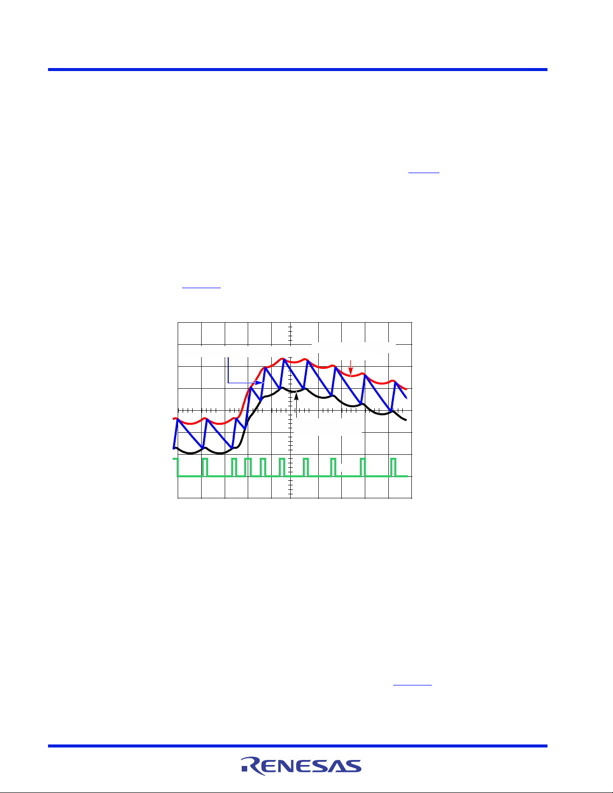
ISL95859C 6. Theory of Operation
Figure 61. Modulator Waveforms During Load Transient
PWM
SYNTHETIC CURRENT SIGNAL
ERROR AMPLIFIER
WINDOW VOLTAGE V
W
(WRT V
COMP
)
VOLTAGE V
COMP
6. Theory of Operation
The ISL95859C is a three output, multiphase controller supporting Intel IMVP8 microprocessor Core (IA), Graphics
(GT), and System Agent (SA), or GTUS rails. The controller supports single-phase operation on outputs VR A and VR C.
Voltage regulator VR B supports 1- or 2-phase operation. The ISL95859C is compliant to Intel IMVP8 specifications with
SerialVID features. The system parameters and SVID required registers are programmable through 2 dedicated
programming pins. This greatly simplifies the system design for various platforms and lowers inventory complexity and
cost by using a single device. The “Typical Application Circuits” section beginning on page 14
view of configuring all three outputs using the ISL95859C controller.
6.1 R3 Modulator
The R3 modulator is Intersil’s proprietary synthetic current-mode hysteretic controller which blends both fixed
frequency PWM and variable frequency hysteretic control technologies. This modulator topology offers high noise
immunity and a rapid transient response to dynamic load scenarios. Under static conditions the desired switching
frequency is maintained within the entire specified range of input voltages, output voltages and load currents.
During load transients the controller will increase or decrease the PWM pulses and switching frequency to maintain
output voltage regulation. Figure 61
climb from a load step, the time between PWM pulses decreases as f
regulation.
illustrates this effect during a load insertion. As the window voltage starts to
increases to keep the output within
SW
provides a top level
CONFIDENTIAL
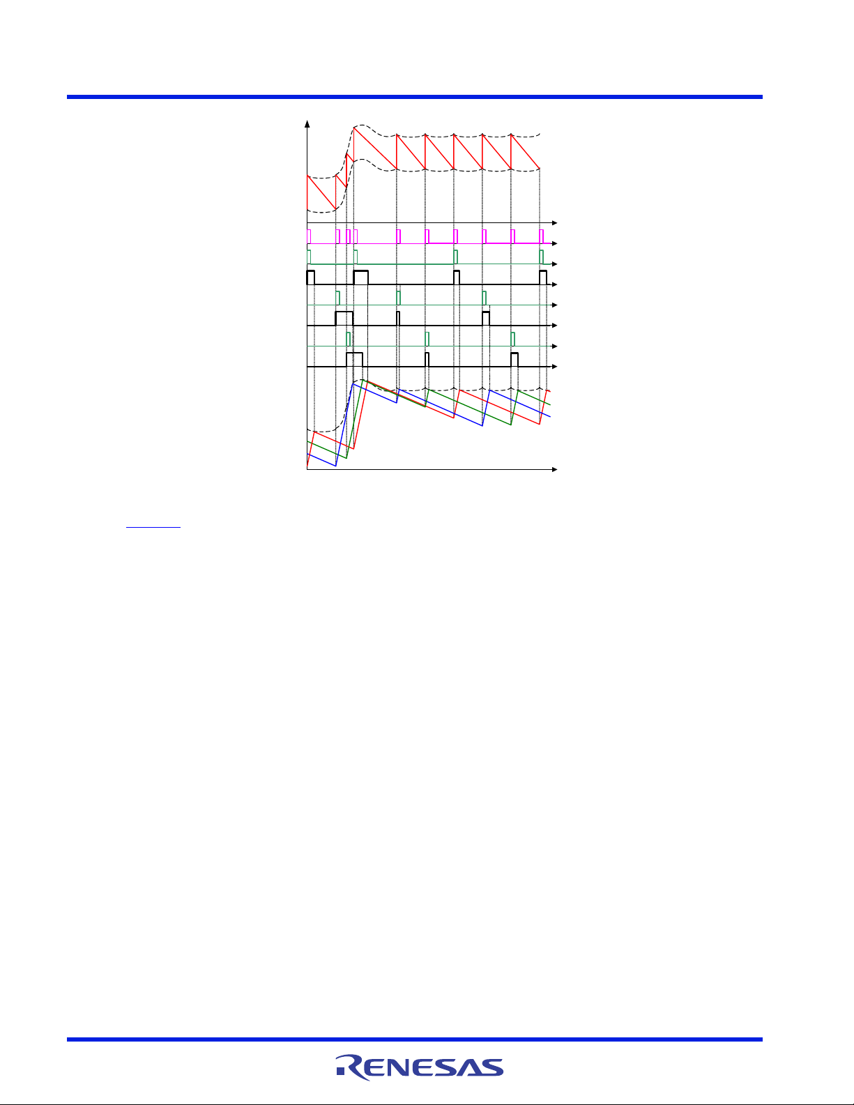
6.2 Multiphase Power Conversion
Microprocessor load current profiles have changed to the point that the advantages of multiphase power conversion
are impossible to ignore. Multiphase converters overcome the daunting technical challenges in producing a costeffective and thermally viable single-phase converter at the high Thermal Design Current (TDC) levels. The
ISL95859C controller VR B output reduces the complexity of multiphase implementation by integrating vital
functions and requiring minimal output components.
6.2.1 Interleaving
The switching of each channel in a multiphase converter is timed to be symmetrically out-of-phase with the
other channels. For the example of a 3-phase converter, each channel switches 1/3 cycle after the previous
channel and 1/3 cycle before the following channel. As a result, the 3-phase converter has a combined ripple
frequency 3x that of the ripple frequency of any one phase, as illustrated in Figure 62
currents (I
, IL2, and IL3) combine to form the AC ripple current and to supply the DC load current.
L1
. The three channel
FN8973 Rev.0.00 Page 23 of 74
Oct 6, 2017

ISL95859C 6. Theory of Operation
I
P-P
VINV
OUT
–V
OUT
Lf
SW
V
IN
----------------------------------------------------------=
(EQ. 1)
Figure 62. PWM and Inductor-Current Waveforms for
3-Phase Converter
1µs/DIV
PWM2, 5V/DIV
PWM3, 5V/DIV
IL2, 7A/DIV
IL3, 7A/DIV
IL1 + IL2 + IL3, 7A/DIV
IL1, 7A/DIV
PWM1, 5V/DIV
The ripple current of a multiphase converter is less than that of a single-phase converter supplying the same
load. To understand why, examine Equation 1
, which represents an individual channel’s peak-to-peak inductor
current.
In Equation 1
value, and f
, VIN and V
is the switching frequency.
SW
are the input and output voltages respectively, L is the single-channel inductor
OUT
CONFIDENTIAL
In a multiphase converter, the output capacitor current is the superposition of the ripple currents from each of the
individual phases. Compare Equation 1
(symmetrically phase-shifted inductor currents) in Equation 2
decreases with the increase in the number of channels, as shown in Figure 63
Ripple Current Multiplier (K
RCM
zero, the turn-off of one phase corresponds exactly with the turn-on of another phase, resulting in the sum of all phase
currents being always the (constant) load current and therefore there is no ripple current in this case.
The output voltage ripple is a function of capacitance, capacitor Equivalent Series Resistance (ESR), and the
summed inductor ripple current. Increased ripple frequency and lower ripple amplitude allow the designer to
use lower saturation-current inductors and fewer or less costly output capacitors for any performance
specification.
to the expression for the peak-to-peak current after the summation of N
. The peak-to-peak overall ripple current (I
C(P-P)
, which introduces the concept of the
). At the steady state duty cycles for which the ripple current and thus the K
)
RCM
is
FN8973 Rev.0.00 Page 24 of 74
Oct 6, 2017

ISL95859C 6. Theory of Operation
DUTY CYCLE (V
OUT/VIN
)
Figure 63. Ripple Current Multiplier vs Duty Cycle
RIPPLE CURRENT MULTIPLIER, K
RCM
N = 1
3
4
2
5
6
0
10 20 30 40 50 60 70 80 90 100
1.0
0
0.9
0.8
0.7
0.6
0.5
0.4
0.3
0.2
0.1
(EQ. 2)
m ROUNDUP N D 0=
for
m1– ND m
I
C(P-P)
V
OUT
LfSW
------------------
K
RCM
=
K
RCM
ND m– 1+mND–
ND
------------------------------------------------------------- ----------------=
Figure 64. Channel Input Currents and Input-Capacitor
RMS Current for 3-phase Converter
CHANNEL 3
INPUT CURRENT
10A/DIV
CHANNEL 2
INPUT CURRENT
10A/DIV
CHANNEL 1
INPUT CURRENT
10A/DIV
INPUT-CAPACITOR CURRENT, 10A/DIV
1µs/DIV
CONFIDENTIAL
Another benefit of interleaving is to reduce the input ripple current. Input capacitance is determined in part by
the maximum input ripple current. Multiphase topologies can improve overall system cost and size by lowering
input ripple current and allowing the designer to reduce the cost of input capacitors. Figure 64
currents from a 3-phase converter combining to reduce the total input ripple current.
FN8973 Rev.0.00 Page 25 of 74
Oct 6, 2017
The converter depicted in Figure 64
current is 5.9A. Compare this to a single-phase converter also stepping down 12V to 1.5V at 36A. The singlephase converter has 11.9A
bank with twice the RMS current capacity as the equivalent 3-phase converter.
A more detailed explanation of input capacitor design is provided in “
input capacitor current. The single-phase converter must use an input capacitor
RMS
illustrates input
delivers 36A to a 1.5V load from a 12V input. The RMS input capacitor
Input Capacitor Selection” on page 37.

ISL95859C 6. Theory of Operation
Figure 65. R3 Modulator Circuit
C
rm
gmVo
MASTER
CLOCK
VW
COMP
MASTER
CLOCK
PHASE
SEQUENCER
CLOCK1
CLOCK2
R
I
L1
gm
CLOCK1
PHASE1
C
rs1
VW
S
Q
PWM1
L1
R
I
L2
gm
CLOCK2
PHASE2
C
rs2
VW
S
Q
PWM2
L2
Co
Vo
Vcrm
Vcrs1
Vcrs2
MASTER CLOCK CIRCUIT
SLAVE CIRCUIT 1
SLAVE CIRCUIT 2
R
I
L3
gm
CLOCK3
PHASE3
C
rs3
VW
S
Q
PWM3
L3
Vcrs3
SLAVE CIRCUIT 3
CLOCK3
+
-
+
-
+
-
+
-
+
-
+
-
+
-
6.2.2 Multiphase R3 Modulator
The Intersil ISL95859C VR B output uses the patented R3 (Robust Ripple Regulator) modulator. The R3
modulator combines the best features of fixed frequency PWM and hysteretic PWM while eliminating many of
their shortcomings. Figure 65
illustrates the operational principles.
shows the conceptual multiphase R3 modulator circuit and Figure 66 on page 27
CONFIDENTIAL
FN8973 Rev.0.00 Page 26 of 74
Oct 6, 2017

ISL95859C 6. Theory of Operation
Figure 66. R3 Modulator Operation Principles in
Steady State
COMP
V
crm
MASTER
CLOCK
PWM1
VW
CLOCK1
PWM2
CLOCK2
HYSTERETIC
WINDOW
PWM3
V
crs3
CLOCK3
V
crs2
V
crs1
VW
The internal modulator uses a master clock circuit to generate the clocks for the slave circuits, one per phase.
CONFIDENTIAL
The R3™ modulator master oscillator slews between two voltage signals; the COMP voltage (the output of the
voltage sense error amplifier, assuming the topology of Figure 76 on page 43
) and VW (Voltage Window), a
voltage positively offset from COMP by an offset voltage that is dependent on the nominal switching frequency.
The modulator discharges the master clock ripple capacitor C
with a current source equal to gmVo, where gm
rm
is a gain factor, dependent on the nominal switching frequency and also on the number of active phases. The
C
voltage V
rm
is a sawtooth waveform traversing between the VW and COMP voltages. It resets (charges
crm
quickly) to VW when it discharges (with discharge current gmVo) to COMP and generates a one-shot master
clock signal. A phase sequencer distributes the master clock signal to the active slave circuits. For example, if
the conceptual VR is in 4-phase mode, the master clock signal is distributed to the four phases 90° out-of-phase,
in 3-phase mode distributed to the three phases 120° out-of-phase, and in 2-phase mode distributed to Phases 1
and 2 180° out-of-phase. If VR is in 1-phase mode, the master clock signal is distributed to Phase 1 only and is
the Clock1 signal.
Each slave circuit has its own ripple capacitor C
, whose voltage mimics the inductor ripple current. A gm
rsn
amplifier converts the inductor voltage (or alternatively, series sense resistor voltage, indicative of that phase’s
inductor current) into a current source to charge and discharge C
upon receiving its respective clock signal Clockn and the current source charges C
proportional to its respective positive inductor voltage. When the C
circuit turns off the PWM pulse and the current source then discharges C
respective now-negative inductor voltage. C
Because the modulator works with the V
discharges until the next Clockn pulse and the cycle repeats.
rsn
, which are large-amplitude and noise-free synthesized signals, it
crsn
. The slave circuit turns on its PWM pulse
rsn
rsn
voltage (V
, with a current proportional to its
rsn
with a current
rsn
) rises to VW, the slave
Crsn
achieves lower phase jitter than conventional hysteretic mode and fixed PWM mode controllers. Unlike
conventional hysteretic mode converters, the ISL95859C uses an error amplifier that allows the controller
outputs to maintain a 0.5% output voltage accuracy.
FN8973 Rev.0.00 Page 27 of 74
Oct 6, 2017
ISL95859C 6. Theory of Operation
Figure 67. R3 Modulator Operation Principles in Load
Insertion Response
COMP
V
crm
MASTER
CLOCK
PWM1
V
crs1
VW
CLOCK1
PWM2
V
crs2
CLOCK2
PWM3
CLOCK3
V
crs3
VW
Figure 67 illustrates the operational principles during load insertion response. The COMP voltage rises during
CONFIDENTIAL
load insertion (due to the sudden discharge of the output capacitor driving the inverting input of the error
amplifier), generating the master clock signal more quickly. Thus, the PWM pulses turn on earlier, increasing
the effective switching frequency. This phenomenon allows for higher control loop bandwidth than
conventional fixed frequency PWM controllers. The VW voltage rises with the COMP voltage, making the
PWM on-time pulses wider. During load release response, the COMP voltage falls. It takes the master clock
circuit longer to generate the next master clock signal so the PWM pulse is held off until needed. The VW
voltage falls with the COMP voltage, reducing the current PWM pulse width. The inherent pulse frequency and
width increase due to an increasing load transient. Likewise, the pulse frequency and width reductions due to a
decreasing load transient produce the excellent load transient response of the R3 modulator.
Because all phases share the same VW window (master clock frequency generator) and threshold (slave pulse
width generator) voltage, dynamic current balance among phases is inherently ensured for the duration of any
load transient event.
The R3 modulator intrinsically has input voltage feed-forward control, due to the proportional dependence of the
clock generator slave transconductance gains on the input voltage. This dependence decreases the on-time
pulse-width of each phase in proportion to an increase in input voltage, making the output voltage insensitive to a fast
slew rate input voltage change.
FN8973 Rev.0.00 Page 28 of 74
Oct 6, 2017

ISL95859C 6. Theory of Operation
UGATE
PHASE
IL
LGATE
Figure 68. Diode Emulation
6.3 Diode Emulation and Period Stretching
The ISL95859C can operate each of its three rails in Diode Emulation Mode (DEM) to improve light-load efficiency.
Diode emulation is enabled in PS2 and PS3 power states. In DEM, the low-side MOSFET conducts while the current
is flowing from source-to-drain and blocks reverse current, emulating a diode. Figure 68
is on, the low-side MOSFET carries current, creating negative voltage on the phase node due to the voltage drop
across the ON-resistance. The controller monitors the inductor current by monitoring the phase node voltage. It turns
off LGATE when the phase node voltage reaches zero to prevent the inductor current from reversing the direction and
creating unnecessary power loss.
illustrates that, when LGATE
If the load current is light enough, as Figure 68
CONFIDENTIAL
next phase node pulse and the regulator is in Discontinuous Conduction Mode (DCM). If the load current is heavy
enough, the inductor current will never reach 0A and the regulator will appear to operate in Continuous Conduction
Mode (CCM), although the controller is nevertheless configured for DEM.
Figure 69
from top to bottom. The PWM on-time is determined by the VW window size, making the inductor current triangle
the same in the three cases (only the time between inductor current triangles changes). The controller clamps the ripple
capacitor voltage V
which produces master clock pulses, naturally stretching the switching period. The inductor current triangles move
further apart from each other such that the inductor current average value is equal to the load current. The reduced
switching frequency improves light-load efficiency.
Because the next clock pulse occurs when V
switching pulse frequency is responsive to load transient events in a manner similar to that of the multiphase CCM
operation.
shows the operation principle in DEM at light load. The load gets incrementally lighter in the three cases
in DEM to make it mimic the inductor current. It takes the COMP voltage longer to hit V
crs
illustrates, the inductor current will reach and stay at zero before the
(which tracks output voltage error) rises above V
COMP
CRM
, DEM
crm
,
FN8973 Rev.0.00 Page 29 of 74
Oct 6, 2017

ISL95859C 6. Theory of Operation
Figure 69. Period Stretching
I
L
I
L
V
crs
I
L
V
crs
V
crs
VW
CCM/DCM BOUNDARY
LIGHT DCM
DEEP DCM
VW
VW
6.4 Adaptive Body Diode Conduction Time Reduction
When in DCM, the controller ideally turns off the low-side MOSFET when the inductor current approaches zero.
CONFIDENTIAL
During on-time of the low-side MOSFET, phase voltage is negative, due to the product of the (negative) inductor
current and the low-side MOSFET r
, producing a voltage drop that is proportional to the inductor current. A
DS(ON)
phase comparator inside the controller monitors the phase voltage during on-time of the low-side MOSFET and
compares it with a threshold to determine the zero-crossing point of the inductor current. If the inductor current has
not reached zero when the low-side MOSFET turns off, it will flow through the low-side MOSFET body diode,
causing the phase node to have a larger voltage drop until it decays to zero. If the inductor current has crossed zero
and reversed the direction when the low-side MOSFET turns off, it will flow through the high-side MOSFET body
diode, causing the phase node to have a positive voltage spike (to V
plus a PN diode voltage drop) until the
IN
current decays to zero. The controller continues monitoring the phase voltage after turning off the low-side
MOSFET and adjusts the phase comparator threshold voltage accordingly in iterative steps such that the low-side
MOSFET body diode conducts for approximately 40ns (turning off 40ns before the inductor current zero-crossing)
to minimize the body diode-related loss.
6.5 Modes of Operation
The ISL95859C controller supports three voltage regulator outputs and each output is configured independently.
VR A and VR C are single-phase only regulators while VR B can support 2-phase or single-phase operation.
6.5.1 VR A Configuration and operation
Voltage Regulator A (VR A) operates only as a single-phase regulator. It operates in 1-phase CCM in PS0 and
PS1 and enters 1-phase DEM in PS2 and PS3. The overcurrent protection level is the same for all power states
as shown in Table 1
Power States Mode OCP Threshold (µA)
01-phase CCM 60
1
21-phase DE
3
FN8973 Rev.0.00 Page 30 of 74
Oct 6, 2017
.
Table 1. VR Modes of Operation VR C

ISL95859C 6. Theory of Operation
6.5.2 VR B Configuration and operation
Voltage Regulator B (VR B) can be configured for 2- or 1-phase operation. Ta ble 2 shows the VR B
configurations and operational modes, programmed by the ISEN2_B and ISEN1_B pin connections and by the
Power State (PS) command (SVID Register 32h). When configured for a 2-phase operation, the ISEN pins must
be connected through a low-pass filter to their respective PHASE node at the output inductor. For a 1-phase
configuration, tie both ISEN1_B and ISEN2_B to VCC. Phases are disabled in order, starting with the highest
numbered phase, as follows.
Table 2. VR Modes of Operation VR B
ISEN2_B Configuration PS Mode OCP Threshold (µA)
To Power Stage 2-phase VR B Configuration 0 2-phase CCM 60
1 1-phase CCM 30
2 1-phase DE
3
Tied to
VCC (+5V)
In a 2-phase configuration, all phases are active and the ISEN2_B and ISEN1_B pins are connected to their
associated PHASE nodes. For a 1-phase configuration, tie the ISEN2_B pin to VCC (+5V) and connect
ISEN1_B to VCC (+5V) or leave it open.
CONFIDENTIAL
In a 2-phase configuration, VR B operates in 2-phase CCM in PS0. It enters 1-phase mode in PS1, PS2, and
PS3 by dropping Phase 2 and reducing the overcurrent protection level to 1/2 of the initial value. PS1 operates
in CCM and PS2 and PS3 operate in DEM.
1-phase VR B Configuration
ISEN1_B open or tied to VCC (+5V)
0 1-phase CCM 60
1
2 1-phase DE
3
In a 1-phase configuration, VR A operates in 1-phase CCM in PS0 and PS1, and enters 1-phase DEM in PS2
and PS3. The overcurrent protection level is the same for all power states.
6.5.3 VR C Operation
Voltage Regulator C (VR C) supports 1-phase operation only. It operates in 1-phase CCM in PS0 and PS1 and
enters 1-phase DEM in PS2 and PS3. The overcurrent protection level is the same for all power states as shown
in Table 3
.
Table 3. VR Modes of Operation VR C
Power States Mode OCP Threshold (µA)
01-phase CCM 60
1
21-phase DE
3
6.5.4 Disabling outputs
Each of the ISL95859C outputs is disabled by connecting the ISUMN_x pin of the voltage regulator to +5V.
The controller will not acknowledge SVID communication to a disabled channel.
FN8973 Rev.0.00 Page 31 of 74
Oct 6, 2017

ISL95859C 6. Theory of Operation
6.6 Programming Resistors
Two programming resistors (R
to set the common switching frequency for the VR A and VR B outputs. The switching frequency options are
450kHz, 583kHz, and 750kHz. This provides flexibility in optimizing the regulators for a wide array of solutions.
R
PROG1
also sets the I
CC(MAX)
maximum current each VR can support. The CPU will read the individual VR I
that the VR current does not exceed the value specified.
Typical PROG1
Resistor
(±1%, KΩ)
1.87 450 21 24 40 18 18
5.62 450 30 30 60 20 20
9.31 450 33 35 40 18 18
13.3 450 34 35 67 18 18
16.9 450 35 40 70 20 20
20.5 450 40 40 75 25 25
24.3 583 21 24 40 18 18
28.0 583 30 30 60 20 20
34.0 583 33 35 40 18 18
41.2 583 34 35 67 18 18
CONFIDENTIAL
48.7 583 35 40 70 20 20
56.2 583 40 40 75 25 25
63.4 750 21 24 40 18 18
71.5 750 30 30 60 20 20
78.7 750 33 35 40 18 18
88.7 750 34 35 67 18 18
100 750 35 40 70 20 20
110 750 40 40 75 25 25
VR A and VR B
Switching Frequency
F
(kHz)
sw
PROG1
and R
) configure the ISL95859C. Table 4 shows how to select R
PROG2
register value for all three VRs. The I
Table 4. PROG1 Pin
VR A VR B VR C
IA/GT 1-ph (A) IA/GT 1-ph (A) IA/GT 2-ph (A) GTUS (A) SA or GTUS (A)
CC(MAX)
IMAX
register value determines the
CC(MAX)
register value and ensure
PROG1
R
sets the address registers for all three VRs (VR A, VR B, and VR C) on the ISL95859C. The three
PROG2
controller outputs can be configured to support three of the four potential processor rails required. The address
selections include Core (IA), Graphics slice (GT), Graphics Unslice (GTUS), and System Agent (SA) rails of the
Intel IMVP8™ processor. The selection should be based on the TDC requirements of the rail and the number of
phases required to support the overall current. Processor SKUs require support for all four processor rails, and the
ISL95859C can be used with the ISL95853 to support them all (see Table 5
R
also selects the switching frequency for VR C. The switching frequency options are 450kHz, 583kHz, and
PROG2
).
750kHz. This provides flexibility in optimizing the regulators for a wide array of solutions.
Table 5. PROG2 Pin
Typical PROG2
Resistor
(±1%, kΩ)
1.87 GT[01h] IA [00h] SA [02h] 450
5.62 GT[01h] IA [00h] SA [02h] 583
9.31 GT[01h] IA [00h] SA [02h] 750
20.5 GT[01h] IA [00h] GTUS [03h] 450
Address
Selection
Switching Frequency
f
SW
VR C
(kHz)VR A VR B VR C
FN8973 Rev.0.00 Page 32 of 74
Oct 6, 2017

ISL95859C 6. Theory of Operation
Table 5. PROG2 Pin (Continued)
Typical PROG2
Resistor
(±1%, kΩ)
24.3 GT[01h] IA [00h] GTUS [03h] 583
28.0 GT[01h] IA [00h] GTUS [03h] 750
48.7 IA [00h] GT[01h] SA [02h] 450
56.2 IA [00h] GT[01h] SA [02h] 583
63.4 IA [00h] GT[01h] SA [02h] 750
88.7 IA [00h] GT[01h] GTUS [03h] 450
100 IA [00h] GT[01h] GTUS [03h] 583
110 IA [00h] GT[01h] GTUS [03h] 750
150 IA [00h] GTUS [03h]] SA [02h] 450
165 IA [00h] GTUS [03h]] SA [02h] 583
182 IA [00h] GTUS [03h]] SA [02h] 750
Address
Selection
Switching Frequency
f
SW
VR C
(kHz)VR A VR B VR C
6.6.1 Switching Frequency Selection
There are a number of variables to consider when choosing switching frequency, as there are considerable effects on
the upper MOSFET loss calculation. These effects are outlined in “
upper limit for the switching frequency. The lower limit is established by the requirement for fast transient response
and small output voltage ripple as outlined in “
frequency that allows the regulator to meet the transient-response and output voltage ripple requirements.
CONFIDENTIAL
The resistors from PROG1 and PROG2 to GND select one of three available switching frequencies: 450kHz,
583kHz, and 750kHz. Note that when the ISL95859C is in Continuous Conduction Mode (CCM), the switching
frequency is not strictly constant due to the nature of the R3 modulator. As explained in “
Modulator” on page 26, the effective switching frequency will increase during load insertion and will decrease
during load release to achieve fast response. However, the switching frequency is nearly constant at constant
load. Variation is expected when the power stage condition, such as input voltage, output voltage, load, etc.
changes. The variation is usually less than 15% and does not have any significant effect on output voltage ripple
magnitude.
Output Filter Design” on page 36. Choose the lowest switching
MOSFETs” on page 34 and they establish the
Multiphase R3
6.7 PSYS System Power Monitoring
In an IMVP8 system the PSYS signal monitors the total system input power from either the battery or adapter.
When implemented according to Intel’s specifications, the PSYS voltage is a 1.2V full-scale analog signal sent into
the PSYS pin of the ISL95859C. The PSYS signal is then digitized and sent to the CPU over the SVID Bus.
This pin is designed to be used in conjunction with Intersil battery chargers. The full-scale current sent to the
ISL95859C PSYS pin from the charger IC should be scaled to a 1.2V full-scale voltage using the appropriate
resistor from the PSYS pin to GND.
FN8973 Rev.0.00 Page 33 of 74
Oct 6, 2017

ISL95859C 7. General Design Guide
P
LOW 1
r
DS ON
I
M
N
------
2
I
P-P
2
12
----------+1d–=
(EQ. 3)
P
LOW 2
V
DONfSW
I
M
N
------
I
P-P
2
----------
–
t
d1
I
M
N
------
I
P-P
2
----------
–
t
d2
+
=
(EQ. 4)
P
LOW 3,
2
3
---
V
IN
1.5
C
OSS_LOWVDS _LOW fSW
(EQ. 5)
7. General Design Guide
This design guide provides a high-level explanation of the steps necessary to design a multiphase power converter. It is
assumed that the reader is familiar with many of the basic skills and techniques referenced in the following. In addition
to this guide, Intersil provides complete reference designs, which include schematics, bills of materials, and example
board layouts for common microprocessor applications.
7.1 Power Stages
The first step in designing a multiphase converter is to determine the number of phases. This determination
depends heavily upon the cost analysis, which in turn depends on system constraints that differ from one design to
the next. Principally, the designer is concerned with whether components can be mounted on both sides of the
circuit board, whether through-hole components are permitted, and the total board space available for power supply
circuitry. Generally speaking, the most economical solutions are those in which each phase handles between 15A
and 25A. In cases where board space is the limiting constraint, current can be pushed as high as 40A per phase, but
these designs require heatsinks and forced air to cool the MOSFETs, inductors, and heat-dissipating surfaces.
7.1.1 MOSFETs
MOSFET choice depends on the current each MOSFET is required to conduct, the switching frequency, the
capability of the MOSFETs to dissipate heat and the availability and nature of heatsinking and air flow.
7.1.1.1 Lower MOSFET Power Calculation
The calculation for heat dissipated in the lower (alternatively called low-side) MOSFET of each phase is
simple, because virtually all of the heat loss in the lower MOSFET is due to current conducted through the
CONFIDENTIAL
channel resistance (r
peak inductor current per phase (see Equation 1 on page 24
channel inductance. Equation 3
). In Equation 3, IM is the maximum continuous output current; I
DS(ON)
); d is the duty cycle (V
shows the approximation.
OUT/VIN
is the peak-to-
P-P
); and L is the per-
A term can be added to the lower MOSFET loss equation to account for the loss during the dead time when
inductor current is flowing through the lower MOSFET body diode. This term is dependent on the diode
forward voltage at I
, V
M
; the switching frequency, fsw; and the length of dead times (td1 and t
D(ON)
d2)
beginning and end of the lower MOSFET conduction interval, respectively.
Finally, the power loss of output capacitance of the lower MOSFET is approximated in Equation 5
where C
OSS_LOW
is the output capacitance of the lower MOSFET at the test voltage of V
DS_LOW
:
. Depending
on the amount of ringing, the actual power dissipation is slightly higher than this.
Thus, the total maximum power dissipated in each lower MOSFET is approximated by the summation of
P
LOW,1
, P
LOW,2
and P
LOW,3
.
7.1.1.2 Upper MOSFET Power Calculation
In addition to r
input voltage (V
dependent on switching frequency, the power calculation is more complex. Upper MOSFET losses are divided
losses, a large portion of the upper MOSFET losses are due to currents conducted across the
DS(ON)
) during switching. Because a substantially higher portion of the upper MOSFET losses are
IN
at the
FN8973 Rev.0.00 Page 34 of 74
Oct 6, 2017

ISL95859C 7. General Design Guide
P
UP 1VIN
I
M
N
------
I
P-P
2
----------+
t
1
2
----
f
SW
(EQ. 6)
P
UP 2VIN
I
M
N
------
I
P-P
2
----------
–
t
2
2
----
f
SW
(EQ. 7)
P
UP 3VINQrrfSW
=
(EQ. 8)
(EQ. 9)
P
UP 4rDS ON
I
M
N
------
2
I
P-P
2
12
----------
+d
P
UP 5LDS
I
M
N
------
I
P-P
2
----------
+
2
(EQ. 10)
P
UP 6
2
3
---
V
IN
1.5
C
OSS_UPVDS_UP fSW
(EQ. 11)
into separate components involving the upper MOSFET switching times, the lower MOSFET body-diode
reverse-recovery charge Q
, and the upper MOSFET r
rr
conduction loss.
DS(ON)
When the upper MOSFET turns off, the lower MOSFET does not conduct any portion of the inductor current
until the voltage at the phase node falls below ground. When the lower MOSFET begins conducting, the current
in the upper MOSFET falls to zero as the current in the lower MOSFET ramps up to assume the full inductor
current. In Equation 6
is P
UP(1)
.
, the required time for this commutation is t1 and the approximated associated power loss
At turn on, the upper MOSFET begins to conduct and this transition occurs over a time (t
approximate power loss is P
A third component involves the lower MOSFET’s reverse-recovery charge, Q
UP(2)
.
. Because the inductor current
rr
). In Equation 7, the
2
has fully commutated to the upper MOSFET before the lower MOSFET’s body diode can draw all of Q
conducted through the upper MOSFET across V
approximated in Equation 8
The resistive part of the upper MOSFET is given in Equation 9
CONFIDENTIAL
Equation 10
accounts for some power loss due to the drain-to-source parasitic inductance (LDS, including PCB
.
. The power dissipated as a result is P
IN
as P
UP(4)
.
UP(3)
and is
parasitic inductance) of the upper MOSFET, although it is not exact:
Finally, the power loss of output capacitance of the upper MOSFET is approximated in Equation 11
:
, it is
rr
where C
is the output capacitance of the lower MOSFET at the V
OSS_UP
test voltage. Depending on the
DS_UP
amount of ringing, the actual power dissipation is slightly higher than this.
The total power dissipated by the upper MOSFET at full load can now be approximated as the summation of the
results from Equations 6
through 11. Because the power equations depend on MOSFET parameters, choosing
the correct MOSFET is an iterative process involving repetitive solutions to the loss equations for different
MOSFETs and different switching frequencies.
7.1.2 Driver Selection
The three voltage regulator outputs of the ISL95859C all feature PWM signals to drive external MOSFET
drivers. Based on the PS4 low quiescent current requirements of the Intel IMVP8 system, only the Intersil
ISL95808 driver or similar device is supported by the controller.
FN8973 Rev.0.00 Page 35 of 74
Oct 6, 2017

ISL95859C 7. General Design Guide
V ESL
di
dt
----- ESRI+
(EQ. 12)
L
ESR
V
OUT
K
RCM
f
SWVIN
V
P-P M A X
----------------------------------------------------------
(EQ. 13)
L
2NCV
OUT
I
2
----------------------------------------- V
MAX
IESR–
(EQ. 14)
L
1.25
NC
I
2
----------------------------- V
MAX
I ESR– VINV
OUT
–
(EQ. 15)
7.2 Output Filter Design
The output inductors and the output capacitor bank together to form a low-pass filter that smooths the pulsating
voltage at the phase nodes. The output filter also must provide the transient energy until the regulator can respond.
Because it has a low bandwidth compared to the switching frequency, the output filter necessarily limits the system
transient response. The output capacitor must supply or sink load current while the current in the output inductors
increases or decreases to meet the demand.
In high-speed converters, the output capacitor bank is usually the most costly (and often the largest) part of the circuit.
Output filter design begins with minimizing the cost of this part of the circuit. The critical load parameters in choosing
the output capacitors are the maximum size of the load step, I; the load-current slew rate, di/dt and the maximum
allowable output voltage deviation under transient loading, V
capacitance, Equivalent Series Resistance (ESR) and Equivalent Series Inductance (ESL).
At the beginning of the load transient, the output capacitors supply all of the transient current. The output voltage will
initially deviate by an amount approximated by the voltage drop across the ESL. As the load current increases, the
voltage drop across the ESR increases linearly until the load current reaches its final value. The capacitors selected must
have sufficiently low ESL and ESR so that the total output voltage deviation is less than the allowable maximum.
Neglecting the contribution of inductor current and regulator response, the output voltage initially deviates by an amount,
as shown in Equation 12
:
. Capacitors are characterized according to their
MAX
The filter capacitor must have sufficiently low ESL and ESR so that V < V
MAX
.
Most capacitor solutions rely on a mixture of high-frequency capacitors with relatively low capacitance in
combination with bulk capacitors having high capacitance but limited high-frequency performance. Minimizing the
CONFIDENTIAL
ESL of the high-frequency capacitors allows them to support the output voltage as the current increases.
Minimizing the ESR of the bulk capacitors allows them to supply the increased current with less output voltage
deviation.
The ESR of the bulk capacitors also creates the majority of the output voltage ripple. As the bulk capacitors sink
and source the inductor AC ripple current (see “
develops across the bulk-capacitor ESR equal to I
maximum allowable ripple voltage, V
Equation 13
.
P-P(MAX)
Interleaving” on page 23 and Equation 2 on page 25), a voltage
(ESR). Thus, when the output capacitors are selected, the
C(P-P)
, determines a lower limit on the inductance as shown in
Because the capacitors are supplying a decreasing portion of the load current while the regulator recovers from the
transient, the capacitor voltage becomes slightly depleted. The output inductors must be capable of assuming the
entire load current before the output voltage decreases more than V
Equation 14
output-voltage deviation than the leading edge. Equation 15
gives the upper limit on L for the cases when the trailing edge of the current transient causes a greater
addresses the leading edge. Normally, the trailing edge
. This places an upper limit on inductance.
MAX
dictates the selection of L because duty cycles are usually less than 50%. Nevertheless, both inequalities should be
evaluated and L should be selected based on the lower of the two results. In each equation, L is the per-channel
inductance, C is the total output capacitance, and N is the number of active channels.
FN8973 Rev.0.00 Page 36 of 74
Oct 6, 2017

ISL95859C 7. General Design Guide
I
IN RMSKIN CM
2
Io2 K
RAMP CM
2
I
Lo(P-P)
2
+=
(EQ. 16)
K
IN CM
ND m– 1+mND–
N
2
--------------------------------------------------------------- -------------=
(EQ. 17)
K
RAMP CM
m2ND m– 1+
3
m1–2mND–
3
+
12N
2D2
--------------------------------------------------------------- ---------------------------------------------------=
(EQ. 18)
0.3
0.1
0
0.2
INPUT CAPACITOR CURRENT (I
RMS
/I
O
)
Figure 70. Normalized Input Capacitor RMS Current
Vs Duty Cycle for 2-Phase Converter
00.4 1.00.2 0.6 0.8
DUTY CYCLE (V
OUT/VIN
)
I
L(P-P)
= 0
I
L(P-P)
= 0.5 I
O
I
L(P-P)
= 0.75 I
O
Figure 71. Normalized Input Capacitor RMS Current
vs Duty Cycle for Single-Phase Converter
00.4 1.00.2 0.6 0.8
DUTY CYCLE (V
OUT/VIN
)
INPUT CAPACITOR CURRENT (I
RMS/
I
O
)
0.6
0.2
0
0.4
I
L(P-P)
= 0
I
L(P-P)
= 0.5 I
O
I
L(P-P)
= 0.75 I
O
7.3 Input Capacitor Selection
The input capacitors are responsible for sourcing the AC component of the input current flowing into the upper
MOSFETs. Their RMS current capacity must be sufficient to handle the AC component of the current drawn by the
upper MOSFETs, which is related to duty cycle and the number of active phases. The input RMS current is
calculated with Equation 16
.
CONFIDENTIAL
For a 2-phase design, use Figure 70 on page 37
duty cycle, maximum sustained output current (I
(I
FN8973 Rev.0.00 Page 37 of 74
Oct 6, 2017
) to IO. Select a bulk capacitor with a ripple current rating that will minimize the total number of input
L(P-P)
capacitors required to support the RMS current calculated. The voltage rating of the capacitors should also be at
least 1.25x greater than the maximum input voltage.
to determine the input capacitor RMS current requirement given the
), and the ratio of the per-phase peak-to-peak inductor current
O

ISL95859C 7. General Design Guide
Figure 72. DCR Current-Sensing Network
C
n
R
sum
R
o
R
ntcs
R
ntc
R
p
DCRLDCR
L
R
sum
R
o
PHASE2 PHASE3
I
O
DCR
L
PHASE1
R
o
R
sum
R
i
ISUMP
ISUMN
Vcn
+
-
For 1-phase designs, use Figure 71 on page 37. Use the same approach to selecting the bulk capacitor type and
number as previously described.
Low capacitance, high-frequency ceramic capacitors are needed in addition to the bulk capacitors to suppress
leading and falling edge voltage spikes resulting from the high current slew rates produced by the upper MOSFETs
turning on and off. Select low ESL ceramic capacitors and place one as close as possible to each upper MOSFET
drain to minimize board parasitic impedances and maximize noise suppression.
7.3.1 Multiphase RMS Improvement
Figure 71 on page 37 demonstrates the dramatic reductions in input-capacitor RMS current upon the
implementation of the multiphase topology. For example, compare the input RMS current requirements of a
2-phase converter versus that of a single-phase. Assume both converters have a duty cycle of 0.25, maximum
sustained output current of 40A, and a ratio of I
17.3A
current capacity, while the 2-phase converter would require only 10.9A
RMS
to IO of 0.5. The single-phase converter would require
L(P-P)
. The advantages become
RMS
even more pronounced when the output current is increased and additional phases are added to keep the
component cost down relative to the single-phase approach.
7.4 Inductor Current Sensing and Balancing
The three VR outputs of the ISL95859C each support a different number of active channels. VR A of the controller
can support up to 3-phase operation, VR B up to 2-phase operation, and VR C is only single phase. Figure 72
the inductor DCR current-sensing network as an example of a 3-phase voltage regulator. The principles described can
be applied to any of the three outputs.
shows
CONFIDENTIAL
7.5 Inductor DCR Current-Sensing Network
Referencing Figure 72, an inductor’s current flows through the inductor’s DCR and creates a voltage drop. Each
inductor has two resistors, R
DCR voltage drop. The R
information to the NTC network (consisting of R
Coefficient (NTC) thermistor that compensates for the change in inductor DCR due to ambient temperature changes
and Ro, connected to its pads to accurately sense the inductor current by sensing the
sum
and Ro resistors are connected in a summing network as shown and feed the total current
sum
ntcs
, R
and Rp) and capacitor Cn. R
ntc
is a Negative Temperature
ntc
and due to power dissipation in the inductor.
The inductor output-side pads are electrically shorted in the schematic but have some parasitic impedance in the actual
board layout, which is why one cannot simply short them together for the current-sensing summing network. It is
recommended to use 1Ω~10ΩR
current sensing circuit, the following analysis will ignore it for simplicity.
FN8973 Rev.0.00 Page 38 of 74
to create quality signals. Because the Ro value is much smaller than the rest of the
o
Oct 6, 2017

ISL95859C 7. General Design Guide
VCns
R
ntcnet
R
ntcnet
R
sum
N
---------------+
------------------------------------------
DCR
N
-------------
I
o
s Acs s=
(EQ. 19)
R
ntcnet
R
ntcsRntc
+Rp
R
ntcsRntcRp
++
----------------------------------------------------=
(EQ. 20)
Acss
1
s
L
-------+
1
s
sns
-------------+
-----------------------=
(EQ. 21)
L
DCR
L
-------------=
(EQ. 22)
sns
1
R
ntcnet
R
sum
N
---------------
R
ntcnet
R
sum
N
---------------+
------------------------------------------
C
n
--------------------------------------------------------=
(EQ. 23)
C
n
L
R
ntcnet
R
sum
N
---------------
R
ntcnet
R
sum
N
---------------+
------------------------------------------
DCR
----------------------------------------------------------- ----=
(EQ. 24)
The summed inductor current information is applied to the capacitor Cn. Equations 19 through 23 describe the
frequency-domain relationship between inductor total current I
(s) and Cn voltage VCn(s):
o
where N is the number of phases.
CONFIDENTIAL
The inductor DCR value increases as the inductor temperature increases, due to the positive temperature coefficient
of the copper windings. If uncompensated, this will cause the estimate of inductor current to increase with
temperature. The resistance of a colocated NTC thermistor, R
compensating for the increase in DCR. Proper selection of the R
V
represents the inductor total DC current over the temperature range of interest.
Cn
, decreases as its temperature increases,
ntc
, R
sum
, Rp, and R
ntcs
parameters ensures that
ntc
Many sets of parameters can properly temperature compensate the DCR change. Because the NTC network and the
R
resistors form a voltage divider, Vcn is always a fraction of the inductor DCR voltage. It is recommended to
sum
have a high ratio of V
to the inductor DCR voltage, so the current sense circuit has a higher signal level to work
cn
with.
A typical set of parameters that provide good temperature compensation are: R
2.61kΩ, and R
= 10kΩ (ERT-J1VR103J). The NTC network parameters may need to be fine-tuned on actual
ntc
= 3.65kΩ, Rp= 11kΩ, R
sum
ntcs
=
boards. One can apply full load DC current and record the output voltage reading immediately, then record the
output voltage reading again when the board has reached the thermal steady state. A good NTC network can limit
the output voltage drift to within 2mV. It is recommended to follow the Intersil evaluation board layout and
current-sensing network parameters to minimize engineering time.
V
(s) response must track Io(s) over a broad range of frequencies for the controller to achieve good transient
Cn
response. Transfer function A
gain at all frequencies, set
(s) (Equation 24) has unity gain at DC, a pole
cs
equal to
L
and solve for Cn.
sns
, and a zero L. To obtain unity
sns
For example, given N = 3, R
L = 0.36µH, Equation 24
FN8973 Rev.0.00 Page 39 of 74
Oct 6, 2017
gives Cn= 0.397µF.
= 3.65kΩ, Rp = 11kΩ, R
sum
= 2.61kΩ, R
ntcs
= 10kΩ, DCR = 0.9mΩ, and
ntc

ISL95859C 7. General Design Guide
V
Cn
I
o
-----------
R
ntcnet
R
ntcnet
R
sum
N
---------------+
------------------------------------------
DCR
N
-------------
=
(EQ. 25)
o
R
ntcnet
R
ntcnet
R
sum
N
---------------+
------------------------------------------
DCR
N
-------------
RoomTemp
=
(EQ. 26)
When the load current I
has a step change, the output voltage V
core
also has a step change, determined by the DC
CORE
load line resistance (the resistor-programmable output voltage droop value, or source resistance, of the regulator).
Assuming the loop compensator design is correct, Figure 80
(see “Verification of Inductor-DCR Current Sense Pole-
Zero Matching” on page 49) shows the expected load transient response waveforms for the correctly chosen value of
C
. If the Cn value is too large or too small, VCn(s) will not accurately represent the real-time Io(s) and the load line
n
transient response will deviate from the ideal. If C
is too small, V
n
will droop excessively (undershoot) upon
CORE
abrupt load insertion before recovering to the intended DC value, which can create a system failure. Similarly, there
is excessive overshoot during load decreases, which can hurt the CPU reliability. If C
is too large, the V
n
CORE
load
line response to load changes will lag.
With the proper selection of C
The value of DCR and R
, assume that Acs(s) = 1. With this assumption, Equation 24 is recast as Equation 25:
n
are both temperature dependent. However, with a properly designed inductor temperature
ntcnet
compensation network, one can also assume the room temperature inductor DCR value and the room temperature value
of R
a variation in the other value. Equation 25
constant value of the ratio V
constant value, designated
, in subsequent calculations, because any temperature variation in one value is, ideally, exactly compensated by
ntcnet
CONFIDENTIAL
Cn/Io
, assumed to be independent of temperature, is required to complete the regulator
is evaluated, using room temperature resistance values, to obtain a
, in units of resistance, for a given DCR current sense network design. This
design.
Equation 26
applies to the DCR current sense circuit of Figure 72 on page 38.
FN8973 Rev.0.00 Page 40 of 74
Oct 6, 2017

ISL95859C 7. General Design Guide
Figure 73. Resistor Current-Sensing Network
C
n
R
sum
R
o
DCRLDCR
L
R
sum
R
o
PHASE2 PHASE3
I
O
DCR
L
PHASE1
R
o
R
sum
R
i
ISUMP
ISUMN
V
cn
R
sen
R
sen
R
sen
+
-
VCns
R
sen
N
-------------
I
o
s A
Rsen
s=
(EQ. 27)
A
Rsen
s
1
1
s
Rsen
-----------------+
---------------------------=
(EQ. 28)
Rsen
1
R
sum
N
---------------
C
n
-----------------------------=
(EQ. 29)
V
Cn
I
o
-----------
R
sen
N
-------------=
(EQ. 30)
o
R
sen
N
-------------=
(EQ. 31)
7.5.1 Resistor Current-Sensing Network
Figure 73 shows the resistor current-sensing network for the example of a 3-phase regulator. Each inductor has
a series current-sensing resistor R
inductor current information. The R
CONFIDENTIAL
for noise attenuation. Equations 27
Transfer function A
significant variation over temperature, so there is no need for the NTC network.
The recommended values are R
As with the DCR current sense network, Equation 29
This equation is evaluated to obtain a constant value of the ratio V
FN8973 Rev.0.00 Page 41 of 74
Oct 6, 2017
current sense network design. This constant value is designated
Equation 31
this constant value is required to complete the regulator design.
applies to the resistor current sense circuit of Figure 73 on page 41. As with the DCR sense design,
. R
sen
and Ro are connected to the R
sum
and Ro resistors are connected to capacitor Cn. R
sum
through 29 give the VCn(s) expression:
(s) always has unity gain at DC. Current-sensing resistor R
Rsen
= 1kΩ and Cn= 5600pF.
sum
is recast as Equation 30:
Cn/Io
pads to accurately capture the
sen
sen
and Cn form a filter
sum
values will not have
, in Ohm units, for a given sense resistor
in Equation 31.

ISL95859C 7. General Design Guide
Figure 74. Droop Illustration
IMON
11
1
/
4
ADC
C
n
V
Cn
...
...
R
i
I
SUMN
I
SUMP
IOUT - SVID
REGISTER 15h
I
droop
R
IMON
+
-
+
-
Ri
o
I
OCP
60A
---------------
=
(EQ. 32)
I
droop
o
R
i
------
I
O
=
(EQ. 33)
7.5.2 Programming of Output Overcurrent Protection, I
, and IMON
droop
The final step in designing the current sense network is the selection of resistor Ri of Figures 72 or 73. This
resistor determines the ratio of the controller’s internal representation of output current (I
, also called the
droop
“droop current”) to the actual output current, that is, to the sum of all the measured inductor currents. This
internal representation is itself a current that is used (a) to compare to the overcurrent protection threshold, (b)
to source the I
current to the FB pin to provide the programmable load-dependent output voltage “droop”
droop
or output DC load line, and (c) to drive the IMON pin external resistor to produce a voltage to represent the output
current. This is measured and written to the IOUT register, readable from the SVID bus.
Begin by selecting the maximum current that the regulator is designed to provide. This is the value of I
programmed with the programming pin resistance to ground for each VR output. Select the appropriate R
to program the lowest available value of I
Protection (OCP) threshold I
I
CC(MAX)
. I
will determine the value of Ri.
OCP
must exceed this value. I
OCP
CC(MAX)
Using VR B as the example, refer to Table 2 on page 31
configuration (1- or 2-phase) and any power state (PS0-PS3) is the threshold value of I
that exceeds the expected maximum load. The Overcurrent
is typically chosen to be 20% to 25% greater than
OCP
. The value of OCP threshold for either phase
that will trigger the
droop
output overcurrent protection. Notice that the OCP threshold value of the PS0 row of any phase configuration is
60µA. R
value of output I
The mechanism by which R
should be chosen such that I
i
, as follows.
OCP
determines I
i
is 60µA when the regulator output current is equal to the chosen
droop
is illustrated in Figure 74.
droop
CONFIDENTIAL
CC(MAX)
PROG1
The ISUM transconductance amplifier produces the current that drops the voltage V
V
directly to the OCP threshold, always 60µA in PS0, so R
Equation 32
where
For a given value of output current, I
FN8973 Rev.0.00 Page 42 of 74
Oct 6, 2017
I
regulator output resistance. Programming of the DC load line is explained in “
Line”.
ISUMN
= V
. This current is mirrored 1:1 to produce I
ISUMP
and 4:1 to produce I
droop
must be chosen to obtain the desired I
i
.
is the constant value determined in Equation 26 or 31.
, I
o
is also used to program the slope of the output DC load line. The DC load line slope is the programmable
droop
will have the value shown in Equation 33:
droop
Programming the DC Load
across Ri, to make
Cn
. I
IMON
is compared
droop
OCP
using

ISL95859C 7. General Design Guide
R
IMON
1.214V
o
I
CC MAX
Ri 4
--------------------------
1–
=
(EQ. 34)
Figure 75. Voltage Regulator Equivalent Circuit
I
O
V
O
VID
Z
OUT
(s) = R
LL
LOAD
VR
+
-
Figure 76. Differential Voltage Sensing and Load Line
Implementation
X 1
E/A
DAC
VID
R
droop
I
droop
VDAC
V
droop
FB
COMP
VCC
SENSE
= V
OUT
VSS
SENSE
VIDs
RTN
VSS
INTERNAL TO IC
CATCH
RESISTOR
CATCH
RESISTOR
VR LOCAL
VOUT
+-
+
+
+
-
-
+
The I
scaled such that its value is 00h when V
R
IMON
current value programmed by R
where again
with R
register (SVID Register 15h) reports an 8-bit unsigned number indicative of the IMON pin voltage,
OUT
is chosen such that V
is the constant value determined in Equation 26 or 31. A capacitor should be added in parallel
to filter the IMON pin voltage and to set the I
IMON
= 1.214V when the regulator load current is equal to I
IMON
PROG2
= 0V and FFh when V
IMON
. Select R
IMON
IMON
using Equation 34:
register response time constant.
OUT
= 1.214V. With Ri determined,
CC(MAX)
, the maximum
7.5.3 Programming the DC Load Line
The DC load line is the effective DC series resistance of the voltage regulator output. The output series
resistance causes the output voltage to “droop” below the selected regulation voltage by a voltage equal to the
load current multiplied by the output resistance. The linear relationship of the output voltage drop to load
current is called the load line and is expressed in units of resistance. It is designated R
. Figure 75 on page 43
LL
shows the equivalent circuit of a voltage regulator (VR) with the droop function. An ideal VR is equivalent to a
voltage source (V = VID) and output impedance Z
output impedance independent of frequency), V
(s). If Z
out
will have a step response when Io has a step change.
O
(s) is equal to the load line slope RLL(constant
out
CONFIDENTIAL
The ISL95859C provides programmable DC load line resistance. A typical desired value of the DC load line for
Intel IMVP8 applications is R
The programmable DC load line mechanism is an integral part of the regulator’s output voltage feedback
compensator. This is illustrated in the feedback circuit and recommended compensation network shown in
Figure 76
FN8973 Rev.0.00 Page 43 of 74
Oct 6, 2017
The ISL95859C implements the DC load line by injecting a current, I
regulator output current I
.
, into the voltage feedback node (the FB pin). The scaling of I
OUT
= 2mΩ.
LL
, which is proportional to the
droop
droop
with respect to

ISL95859C 7. General Design Guide
V
droopRLLIo
=
(EQ. 35)
V
droopIdroopRdroop
o
Ri
------
I
o
R
droop
==
(EQ. 36)
R
droop
Ri RLL
o
-----------------------=
(EQ. 37)
Figure 77. Duty Cycle Balancing Circuit
INTERNAL
TO IC
V
o
ISEN3
L
3
R
isen
C
isen
ISEN2
R
isen
C
isen
ISEN1
R
isen
C
isen
L
2
L
1
R
dcr3
R
dcr2
R
dcr1
PHASE3
PHASE2
PHASE1
I
L3
I
L2
I
L1
R
pcb3
R
pcb2
R
pcb1
V3p
V2p
V1p
I
was selected in “Programming of Output Overcurrent Protection, Idroop, and IMON” on page 42 to
OUT
obtain the desired output I
R
, between the FB pin and the output voltage due to I
droop
the FB pin.) R
raised above V
is selected to implement the desired DC load line resistance RLL. The FB pin voltage is thus
droop
by the droop voltage, requiring the regulator to reduce V
OUT
threshold. The droop voltage is the voltage drop across the resistance, called
OCP
droop
. (R
is the only DC path between V
droop
to make VFB equal to the
OUT
OUT
and
voltage regulator reference voltage applied to the error amplifier noninverting input.
R
is a component of the voltage regulator stability compensation network. The regulator stability and
droop
dynamic response is determined independently of the value of R
the COMP-to-FB capacitance and the series RC in parallel with R
at and well below the open loop crossover frequency. Because R
, because the loop integral gain is set with
droop
will dominate the compensator response
droop
plays a singular role in determining the
droop
DC load line, it is chosen solely for that purpose.
For a desired R
Equation 35
, the output voltage reduction, V
LL
.
, due to an output load current, Io, is as shown in
droop
The value of V
droop resistor, R
obtained from the ISL95859C controller is the droop current, I
droop
. Using Equation 33, this value is as shown in Equation 36.
droop
Equate these two expressions for V
and solve for R
droop
to obtain the value in Equation 37.
droop
, multiplied by the
droop
CONFIDENTIAL
7.5.4 Phase DC Voltage and Current Balancing
To equally distribute power dissipation between the active phases of a VR, the controller provides a means to
reduce the deviation of the DC component (approximately the product of the duty cycle and V
phase voltage from the average of all phases’ DC voltages. The controller achieves phase node DC voltage
balance by continually trimming the modulator slave circuits to match the ISENn pin voltages. The connection
of these pins to their respective phase nodes is depicted in Figure 77
for the inductor DCR current sense method,
for the example of a three phase VR. The DC voltage and current balancing methods described in this section
apply also to current sensing using discrete sense resistors.
VIN
) of each
FN8973 Rev.0.00 Page 44 of 74
Oct 6, 2017
The phase nodes have high amplitude square-wave voltage waveforms, for which the DC component is
indicative of each phase’s relative contribution to the output. R
and C
isen
form low-pass filters to remove the
isen

ISL95859C 7. General Design Guide
V
ISEN1
R
dcr1Rpcb1
+IL1 Vo+=
(EQ. 38)
V
ISEN2
R
dcr2Rpcb2
+IL2 Vo+=
(EQ. 39)
V
ISEN3
R
dcr3Rpcb3
+IL3 Vo+=
(EQ. 40)
switching ripple of the phase node voltages, such that the voltages at the ISENn pins approximately indicate
each phase’s DC voltage component and thus the relative contribution of each phase to the output current. The
controller gradually and continually trims the R3 modulator slave circuits. Thus, adjusting the relative duty cycle
of each phase reduces the phase node DC voltage differences, as indicated by each V
. This adjustment
ISENn
occurs slowly compared to the dynamic response of the multiphase modulator to output voltage commands,
load transients, power state changes and other system perturbations.
It is recommended to use a large R
isenCisen
time constant, such that the ISENn voltages have small ripple and
are representative of the average or steady-state contribution of each phase to the output. Recommended values
are R
= 10kΩ and C
isen
isen
= 0.22µF.
Ideally, balancing the phase nodes’ average (DC) voltages will also balance the output current provided by each
phase and the power dissipated in each phase’s components. This is the case if the current sense elements of
each phase are identical (DCR of the inductors, or discrete current sense resistors and the associated current
sense networks) and if parasitic resistances of the circuit board traces from the sense connections to the
common output voltage node are identical. Figure 77
shows the printed circuit trace resistances from each phase
to the common output node. If these trace resistances are all equal, then the ideal of phase current balance is
achieved with this design. This balance assumes the inductors and other current sense components are identical,
comparing each phase to the others, a true assumption within the published tolerance of component parameters.
Figure 77
MOSFET switches to the inductor. This is correct assuming that each R
includes the trace-resistance from each inductor to a single common output node, but not from the
connection (V1p, V2p and V3p) is
isen
routed directly to its respective inductor phase-node-side pad in order to eliminate the effect of phase node
parasitic PCB resistance from the switching elements to the inductor. Equations 38
through 40 give the ISEN pin
voltages:
CONFIDENTIAL
, R
where R
dcr1
dcr2
, and R
parasitic PCB resistances between the inductor output-side pad and the output voltage rail; and I
are the respective inductor DCRs; R
dcr3
pcb1
, R
pcb2
, and R
are the respective
pcb3
L1
, IL2, and IL3
are inductor average currents.
The phase balance controller will adjust the phase pulse-width relative to the other phases to make
V
ISEN1=VISEN2=VISEN3
Because using the same components for L1, L2, and L3 will typically provide a good match of R
R
, board layout will determine R
dcr3
, thus obtaining IL1=IL2=IL3 if R
, R
pcb1
pcb2
, and R
and thus the matching of current per phase. It is
pcb3
dcr1=Rdcr2=Rdcr3
and R
pcb1=Rpcb2=Rpcb3
dcr1
, R
dcr2
.
, and
recommended to have symmetrical layout for the power delivery path between each inductor and the output
voltage rail, such that R
pcb1=Rpcb2=Rpcb3
.
While careful symmetrical layout of the circuit board can achieve very good matching of these trace resistances,
such layout is often difficult to achieve in practice. If trace resistances differ, then exact matching the phases’
DC voltages will result in the imbalance of the phase currents. A modification of this circuit (to couple the
signals of all the phases in the ISENn networks) can correct the current imbalance due to unequal trace
resistances to the output.
For the example case of a 3-phase configuration, Figure 78 on page 46
shows the phase balancing circuit with
the recommended trace-resistance imbalance correction. As before, V1p, V2p, and V3p should be routed to their
respective inductor phase-node-side pads in order to eliminate the effect of phase node parasitic PCB resistance
from the switching elements to each inductor. The sensing traces for V1n, V2n, and V3n should be routed to the
FN8973 Rev.0.00 Page 45 of 74
Oct 6, 2017

ISL95859C 7. General Design Guide
Figure 78. Differential Sensing Current Balancing Circuit
INTERNAL
TO IC
V
o
ISEN3
L
3
R
isen
C
isen
ISEN2
R
isen
C
isen
ISEN1
R
isen
C
isen
L
2
L
1
R
dcr3
R
dcr2
R
dcr1
PHASE3
PHASE2
PHASE1
I
L3
I
L2
I
L1
R
pcb3
R
pcb2
R
pcb1
R
isen
R
isen
R
isen
R
isen
R
isen
R
isen
V3p
V3n
V2p
V2n
V1p
V1n
V
ISEN1
V1pV2nV
3n
++
3
-------------------------------------------------=
(EQ. 41)
V
ISEN2
V1nV2pV
3n
++
3
-------------------------------------------------=
(EQ. 42)
V
ISEN3
V1nV2nV
3p
++
3
-------------------------------------------------=
(EQ. 43)
V1pV2nV
3n
++ V1nV2pV
3n
++=
(EQ. 44)
V1nV2pV
3n
++ V1nV2nV
3p
++=
(EQ. 45)
V1pV1n– V2pV2n–=
(EQ. 46)
V2pV2n– V3pV3n–=
(EQ. 47)
V
output-side inductor pads so they sense the voltage due only to the voltage drop across the inductor DCR
OUT
and not due to the PCB trace resistance.
Each ISEN pin sees the average voltage of three sources: its own phase inductor phase-node pad and the other
two phases inductor output-side pads. Equations 41
through 43 give the ISEN pin voltages:
CONFIDENTIAL
The controller will make V
Simplifying Equation 44
FN8973 Rev.0.00 Page 46 of 74
Oct 6, 2017
and simplifying Equation 45
gives Equation 46:
= V
ISEN1
gives Equation 47:
ISEN2
= V
, resulting in the equalities shown in Equations 44 and 45:
ISEN3

ISL95859C 7. General Design Guide
V1pV1n– V2pV2n– V3pV3n–==
(EQ. 48)
R
dcr1IL1
R
dcr2IL2
R
dcr3IL3
==
(EQ. 49)
Combining Equations 46 and 47 gives Equation 48:
which produces the desired result in Equation 49
Current balancing (I
within the tolerance of the resistance of the current sense elements. Note that with the cross coupling of
Figure 79
equalizes the DC components of the voltage drops across the current sense elements.
Small absolute differences in PCB trace resistance from the inductors to the common output node can result in
significant phase current imbalance. It is strongly recommended that the resistor pads and connections for the
cross-coupling current balancing method be included in any PCB layout. The decision to include the additional
Nx(N-1) trace-resistance correcting resistors can then be deferred until the extent of the current imbalance is
measured on a functioning circuit. Considerations for making this decision are described in “
Balancing” on page 51.
With the ISENn phase balancing mechanism (with cross coupling resistors if needed, or without if not needed), the
R3™ modulator achieves excellent current balancing during both steady state and transient operation. Figure 79
shows current balancing performance of an evaluation board with load transient of 12A/51A at different rep
rates. The inductor currents follow the load current dynamic change with the output capacitors supplying the
difference. The inductor currents can track the load current well at low rep rate, but cannot track the load when
CONFIDENTIAL
the rep rate gets into the 100kHz range, which is outside of the control loop bandwidth. Regardless, the
controller achieves excellent current balancing in all cases.
, the phase balancing circuit no longer equalizes the average voltage of the phase nodes, but rather
L1=IL2=IL3
) is achieved independently of any mismatch of R
:
, R
pcb1
, and R
pcb2
Phase Current
pcb3
to
FN8973 Rev.0.00 Page 47 of 74
Oct 6, 2017

ISL95859C 7. General Design Guide
REP RATE = 10kHz
REP RATE = 25kHz
REP RATE = 50kHz
REP RATE = 100kHz
REP RATE = 200kHz
CONFIDENTIAL
Figure 79. Current Balancing During Dynamic Operation. CH1: IL1, CH2: I
FN8973 Rev.0.00 Page 48 of 74
Oct 6, 2017
, CH3: IL2, CH4: I
LOAD
L3

ISL95859C 7. General Design Guide
Figure 80. Desired Load Transient Response Waveforms
O
I
V
O
Figure 81. Load Transient Response When Cn is too Large
O
I
V
O
Figure 82. Load Transient Response When Cn is too Small
O
I
V
O
7.6 Current Sense Circuit Adjustments
When a voltage regulator (VR) is designed and a functional prototype has been assembled, adjustments may be
necessary to correct for non-ideal components or assembly and printed circuit board parasitic effects. These are
effects that are usually not known until the design has been realized. The following adjustments should be
considered when refining a product design.
7.6.1 Verification of Inductor-DCR Current Sense Pole-Zero Matching
Recall that if the inductor DCR is used as the phase current sense element, it is necessary to select the capacitor
C
such that the current sense transfer function pole at
n
step, with DC load line (“droop”) enabled, is shown in Figure 80
matches the zero at L. The ideal response to a load
sns
.
Figure 81
lags in settling to its final value.
CONFIDENTIAL
Figure 82
shows the load step transient response when Cn is too large. V
shows the load step response when Cn is too small. V
response is underdamped and overshoots
CORE
droop response (rising or falling)
CORE
before settling to its final voltage.
When the regulator design is complete, the measured load step response is compared to Figures 80
C
should be adjusted if necessary to obtain the behavior of Figure 80.
n
FN8973 Rev.0.00 Page 49 of 74
Oct 6, 2017
through 82.

ISL95859C 7. General Design Guide
7.6.2 Current Sense Sensitivity Error
The current sense, IMON and DC load line (droop) network component values should be designed according to
the instructions in “
“
Programming the DC Load Line” on page 43. This will ensure the correct ratio of V
determines R
However, testing of the resulting circuit may reveal a measurement sensitivity error factor, which should effect
V
and I
IMON
as a too-large IMON voltage for a given load current. A single component modification will correct both errors.
The current sense resistance value per phase (either a discrete sense resistor, or the inductor DCR) is typically
very small, on the order of 1mΩ. The solder connections used in the assembly of such sense elements may
contribute significant resistance to these sense elements, resulting in a larger load-dependent voltage drop than
due to the sense element alone. Thus, the sensed output current value is greater than intended for a given load
current. If this is the case, then the value of R
sensitivity error. For example, if the current sense value is 3% larger than intended, then R
by 3%. Changing R
thus simultaneously correcting the IMON voltage error and the load line resistance, while preserving the
intended ratio between the two parameters.
Note that the assembly procedure for installing the current sense elements (sense resistors or inductors) can
have a significant impact on the effective total resistance of each sense element. It is important that any
adjustments to R
in mass production. The current measurement sensitivity error should be determined on a sufficient number of
samples to avoid adjusting sensitivity to correct what may be a component-tolerance outlier.
Programming of Output Overcurrent Protection, Idroop, and IMON” on page 42 and
to I
and I
IMON
should be increased
i
by the same factor,
droop
) for the chosen system design parameters, for which no adjustment should be required.
LL
equally. This error may be seen as a too-large RLL value (droop voltage per load current) and
droop
(the ISUMN pin resistor) should be increased by the factor of the
i
will change the sensitivity (with respect to I
i
be performed on circuits that have been assembled with the same procedures that will be used
i
OUT
) of V
IMON
droop
(which
CONFIDENTIAL
7.6.3 DCR Current Sense OFFSET Error
When using the inductor DCR current sensing, nonlinearity of the R
offset in the ISUMP voltage and thus, in the IMON pin current (viewed as a positive offset in the ICC register
value) and also in the droop current (viewed as an output voltage negative offset). The offset error occurs as
follows: for each inductor, the instantaneous voltage across its R
V
RSUM=VPHASE-VVOUT
During the off time, V
V
= 12V, V
VIN
RSUM-ON
. During that phase’s on time, V
= 0V and so V
PHASE
= 10.2V and V
RSUM-OFF
RSUM-OFF
= –V
= –1.8V, a sign-dependent magnitude difference exceeding
SUM
PHASE=VVIN
VOUT
8V. Inexpensive thick film resistors can have a voltage nonlinearity of 25ppm/volt or more, with the device
resistance decreasing with increasing voltage. Because of this R
SUM
(positive) current into the common ISUMP node (during its on-time) is biased slightly greater than the nominal
V/R value expected. Each R
the resistor nonlinearity, but less so because the R
’s (negative) current (during its off-time) will also be biased negatively due to
SUM
voltage magnitude is always much less during the
SUM
off-time than during the on-time. This nonlinearity bias current polarity mismatch causes a small positive offset
error in V
. Note that this offset error will not occur if using discrete resistors as current sense elements.
ISUMP
The exact magnitude of this offset error is difficult to predict. It depends on an attribute of the sense resistors
that is typically not specified or controlled and so not reliably quantified. It also varies with the input voltage
and the output voltage. If battery powered, the input voltage can vary significantly. The output voltage is subject
to the VID setting and to a lesser extent on the droop voltage. A further complication is that the nonlinearity
offset changes with the number of active phases. For a 3-phase configuration in PS0, three R
subjected to the high difference in on-time compared to off-time voltage magnitudes. But in PS1, one or two
phases are disabled (based on the PROG2 setting) with the respective PHASE nodes approximately following
the output. Thus, V
for the disabled phases is approximately zero for the entire switching cycle, reducing
RSUM
the offset error by 1/3 to 2/3. In PS2, only one phase is active and two phases are disabled, leaving only a third
of the PS0 offset error.
The most direct solution to the phenomenon of current sense offset due to resistor nonlinearity is to use highly
linear summing resistors, such as thin film resistors. But the magnitude of the offset error typically does not
resistors can induce a small positive
SUM
resistor is approximately
, giving V
RSUM-ON
. For the example of V
= V
VOUT
resistor nonlinearity, each R
SUM
VIN
= 1.8V and
SUM
resistors are
– V
’s
VOUT
.
FN8973 Rev.0.00 Page 50 of 74
Oct 6, 2017

ISL95859C 7. General Design Guide
warrant the considerably greater expense of doing so. Instead, a correcting fixed offset is introduced to the
current sense network.
For the example case described, with each thick film R
current sense offset error in PS0 typically represents less than 1% of full scale and is always positive. It has
been found empirically that a 10MΩ pull-down resistor from the ISUMP node to ground provides a good
correcting offset compromise slightly undercorrecting in PS0 and slightly overcorrecting in PS2, but meeting
processor vendor specification tolerances with adequate margin in all cases. For other applications, a suitable
compromise pull-down resistor is determined empirically by testing over the full range of expected operating
conditions and power states. It is recommended that this resistor be included in any VR design layout to allow
population of the pull-down resistor if required. Because of the high value of resistance, two smaller valued
resistors in series may be preferred, to reduce the environmental sensitivity of high resistance value devices.
= 3.65kΩ and an I
SUM
CC(MAX)
setting of 100A, the
7.6.4 Phase Current Balancing
Phase current imbalance should be measured on a functioning circuit. First, verify the correct assembly of the
current balancing mechanism by measuring, on a stable operating regulator, the voltage difference between the
ISEN1 pin and the remaining ISENn pins (of all the operational phases) with various static loads applied.
Whether using the simple circuit of Figure 77 on page 44
Figure 77
than 1mV. If not, there may be an assembly error.
Then, again with various static loads applied, measure the voltage directly across each active sense element
(sense resistor or inductor). Any discrepancy in the phase sense element voltages beyond what is attributed to
the sense element resistance tolerance must be due to PCB trace resistance deviations. Install the cross-coupling
resistors shown in Figure 83
CONFIDENTIAL
should be the same among the phases in all cases (to within the tolerance of the cross coupling resistors) and the
phase current balance is within the parametric tolerance of the sense element resistance, independently of the
PCB trace resistance differences.
The decision to populate the cross-coupling phase sense resistors will depend upon the magnitude and system
tolerance of the uncorrected imbalance current.
, the voltage difference between any pair of the ISENn pins should be very small, usually less
and again compare the sense element voltages. Now the sense element voltages
or the PCB trace resistance compensating circuit of
7.6.5 Load Step Ringback
Figure 83 shows the output voltage ringback problem during load transient response with DC load line
(“droop”) enabled. The load current I
follow. Instead, I
effect of the output capacitors makes the output voltage V
controller regulates V
responds in first order system fashion due to the nature of current loop. The ESR and ESL
L
according to the droop current I
O
has a fast step change, but the inductor current IL cannot accurately
O
dip quickly upon load current change. However, the
O
, which is a real-time representation of IL.
droop
FN8973 Rev.0.00 Page 51 of 74
Oct 6, 2017

ISL95859C 7. General Design Guide
Figure 83. Output Voltage Ringback Problem
O
I
V
O
L
I
RINGBACK
Figure 84. Optional Circuits for Ringback Reduction
C
n.2
R
ntcs
R
ntc
R
p
R
i
ISUMP
ISUMN
R
ip
C
ip
V
cn
C
n.1
R
n
OPTIONAL
+
-
Therefore it pulls VO back to the level dictated by IL, causing the ringback problem. This phenomenon is not
observed when the output capacitor bank has very low ESR and ESL, such as if using only ceramic capacitors.
CONFIDENTIAL
OPTIONAL
Figure 84
C
n
to get the desired value. Figure 84 on page 52
R
n
capacitance. At the beginning of I
impedance of the C
effect will reduce the V
more pronounced when R
too small. It is recommended to keep C
and R
system circuit board.
R
ip
of I
values, I
100Ω. C
recommended range for C
the I
may adversely affect I
shows two optional circuits for reduction of the ringback.
is the capacitor used to match the inductor time constant. It often takes the paralleling of multiple capacitors
shows that two capacitors C
is an optional component to reduce the VO ringback. At steady state, C
change, the effective capacitance is less because Rn increases the
branch. As Figure 82 on page 49 shows, VO tends to dip when Cn is too small and this
n.1
ringback. This effect is more pronounced when C
O
n
values should be determined through tuning the load transient response waveforms directly on the target
n
O
is bigger. However, the presence of Rn increases the ripple of the Vn signal if C
greater than 2200pF. The Rn value is usually a few ohms. C
n.2
and C
n.1
+ C
n.1
is much larger than C
n.1
are in parallel. Resistor
n.2
provides the desired Cn
n.2
. It is also
n.2
n.1
, C
n.2
is
n.2
and Cip form an R-C branch in parallel with Ri, providing a lower impedance path than Ri at the beginning
change. Rip and Cip do not have any effect at steady state. Through proper selection of Rip and Cip
OUT
droop
can resemble I
droop
should be determined by observing the load transient response waveforms in a physical circuit. The
ip
waveform. Instead of being triangular as the real inductor current, I
droop
rather than IL and VO will not ring back. The recommended value for Rip is
OUT
is 100pF~2000pF. However, it should be noted that the Rip-Cip branch can distort
ip
may have sharp spikes, which
droop
average value detection and therefore may affect OCP accuracy.
,
FN8973 Rev.0.00 Page 52 of 74
Oct 6, 2017

ISL95859C 7. General Design Guide
Figure 85. Loop Gain T1(s) Measurement Setup
Q2
Q1
L
I
O
C
OUT
V
O
V
IN
GATE
DRIVER
COMP
MOD.
LOAD LINE SLOPE
EA
VID
CHANNEL BCHANNEL A
EXCITATION OUTPUT
ISOLATION
TRANSFORMER
LOOP GAIN =
CHANNEL B
CHANNEL A
NETWORK
ANALYZER
-
+
+
+
20
7.7 Voltage Regulation
7.7.1 Compensator
Intersil provides a Microsoft Excel-based spreadsheet to help design the compensator and the current sensing
network for each output of the ISL95859C. The spreadsheet helps in designing each VR to achieve constant output
impedance as a stable system. Visit www.intersil.com/en/support
A VR with active droop function is a dual-loop system consisting of a voltage loop and a droop loop, which is a
current loop. However, neither loop alone is sufficient to describe the entire system. The spreadsheet shows two
loop gain transfer functions, T1(s) and T2(s), that describe the entire system. Figure 85
measurement setup and Figure 86
conceptually shows T2(s) measurement setup. The VR senses the inductor
current, multiplies it by a gain of the load line slope, then adds it on top of the sensed output voltage and feeds it to
the compensator. T1(s) is measured after the summing node and T2(s) is measured in the voltage loop before the
summing node. The spreadsheet gives both T1(s) and T2(s) plots. However, only T2(s) is actually measured on an
ISL95859C regulator.
T1(s) is the total loop gain of the voltage loop and the droop loop. It always has a higher crossover frequency
than T2(s) and has more impact on system stability.
T2(s) is the voltage loop gain with closed droop loop. It has more impact on output voltage response.
Design the compensator to get stable T1(s) and T2(s) with sufficient phase margin and output impedance equal
or smaller than the load line slope.
to request the spreadsheet for the ISL95859C.
conceptually shows T1(s)
CONFIDENTIAL
FN8973 Rev.0.00 Page 53 of 74
Oct 6, 2017

ISL95859C 7. General Design Guide
Figure 86. Loop Gain T2(S) Measurement Setup
Q2
Q1
L
O
I
C
OUT
V
O
V
IN
GATE
DRIVER
COMP
MOD.
LOAD LINE SLOPE
EA
VID
CHANNEL BCHANNEL A
EXCITATION OUTPUT
ISOLATI ON
TRANSFORMER
20
LOOP GAIN=
CHANNEL B
CHANNEL A
NETWORK
ANALYZER
-
+
+
+
Figure 87. SA Soft-Start Waveforms
VCC
VR_ENABLE
DAC
704µs
DVID-SLOW
V
BOOT
VR_READY
ALERT#
...
7.7.2 Start-up Timing
With the controller's VCC voltage above the POR threshold, the start-up sequence begins when VR_ENABLE
exceeds the logic high threshold. Figure 87
the controller if VRC is configured as the SA rail. The SA rail must soft-start to a V
other three potential address options (IA, GT, or GTUS) all V
CONFIDENTIAL
The VR_READY signal is asserted high when the controller is initialized and able to receive SVID commands,
within 704µs after VR_ENABLE is asserted high as reported by SVID register index 2Dh. VR_READY
remains high until either VR_ENABLE is deasserted, or until a fault is detected on any of the VRs.
VR_READY also indicates when VRC (if configured as the SA rail) begins incrementally stepping its DAC
from 0V to V
at a rate equivalent to a SetVID_slow command (for a precharged output, the DAC begins
BOOT
incrementally stepping from the output’s initial voltage). At the end of the SA rail DAC ramp to V
ALERT# is asserted low, as it would for any SetVID command completion.
shows the typical start-up timing for the System Agent (SA) rail of
voltage of 1.05V. The
to 0V per IMVP8 specifications.
BOOT
BOOT
BOOT
,
Similar behavior occurs if VR_ENABLE is tied directly to V
and V
7.7.3 Voltage Regulation
After the start-up sequence, the controller regulates the three output voltages to the value set by the VID
information per Table 6 on page 55
±0.5% over the VID voltage range. A differential amplifier allows voltage sensing for precise voltage regulation
at the microprocessor die.
FN8973 Rev.0.00 Page 54 of 74
Oct 6, 2017
voltages exceed their respective POR rising thresholds.
IN
. The start-up sequence begins after both VCC
CC
. The controller will control the no load output voltages to an accuracy of

ISL95859C 7. General Design Guide
(EQ. 50)
VCC
SENSE
V+
droop
V
DAC
VSS
SENSE
+=
VCC
SENSE
VSS
SENSE
– V
DACRdroopIdroop
–=
(EQ. 51)
This mechanism is illustrated in Figure 76 on page 43. VCC
signals from the processor die. A unity gain differential amplifier senses the VSS
SENSE
and VSS
are the remote voltage sensing
SENSE
voltage and adds it to the
SENSE
DAC output. Note how the illustrated DC load line mechanism (the “droop” mechanism, described in
“
Programming the DC Load Line” on page 43), introduces a load-dependent reduction in the output voltage,
(denoted VCC
the noninverting input voltages to be equal, as shown in Equation 50
Rewriting Equation 50
Equation 51
CONFIDENTIAL
The VCC
is the ideal relationship required for load line implementation.
SENSE
the processor. As shown in Figure 76 on page 43
), below the VID value output by the DAC. The error amplifier regulates the inverting and
SENSE
:
and substituting Equation 36 gives Equation 51:
and VSS
signals are sensed at the processor die. The feedback is open circuit in the absence of
SENSE
, it is recommended to add a “catch” resistor to feed the VR local
output voltage back to the compensator and add another “catch” resistor to connect the VR local output ground to the
RTN pin. These resistors, typically 10Ω~100Ω, will provide voltage feedback if the system is powered up without a
processor installed.
The maximum VID (output voltage command) value supported is 1.52V. Any VID command (or sum of VID
command and VID offset) above 2.3V is ignored.
Table 6. VID Table
VID
HEX V
0 0 0 0 0 0 0 0 0 0 0.00000
0 0 0 0 0 0 0 1 0 1 0.25000
0 0 0 0 0 0 1 0 0 2 0.25500
0 0 0 0 0 0 1 1 0 3 0.26000
0 0 0 0 0 1 0 0 0 4 0.26500
0 0 0 0 0 1 0 1 0 5 0.27000
0 0 0 0 0 1 1 0 0 6 0.27500
0 0 0 0 0 1 1 1 0 7 0.28000
0 0 0 0 1 0 0 0 0 8 0.28500
0 0 0 0 1 0 0 1 0 9 0.29000
0 0 0 0 1 0 1 0 0 A 0.29500
0 0 0 0 1 0 1 1 0 B 0.30000
0 0 001 1 000C 0.30500
(V)76543210
O
FN8973 Rev.0.00 Page 55 of 74
Oct 6, 2017

ISL95859C 7. General Design Guide
Table 6. VID Table (Continued)
VID
HEX V
0 0 001 1 010D 0.31000
0 0 0 0 1 1 1 0 0 E 0.31500
0 0 0 0 1 1 1 1 0 F 0.32000
0 0 0 1 0 0 0 0 1 0 0.32500
0 0 0 1 0 0 0 1 1 1 0.33000
0 0 0 1 0 0 1 0 1 2 0.33500
0 0 0 1 0 0 1 1 1 3 0.34000
0 0 0 1 0 1 0 0 1 4 0.34500
0 0 0 1 0 1 0 1 1 5 0.35000
0 0 0 1 0 1 1 0 1 6 0.35500
0 0 0 1 0 1 1 1 1 7 0.36000
0 0 0 1 1 0 0 0 1 8 0.36500
0 0 0 1 1 0 0 1 1 9 0.37000
0 0 0 1 1 0 1 0 1 A 0.37500
0 0 0 1 1 0 1 1 1 B 0.38000
CONFIDENTIAL
0 0 011 1 001C 0.38500
0 0 011 1 011D 0.39000
0 0 0 1 1 1 1 0 1 E 0.39500
0 0 0 1 1 1 1 1 1 F 0.40000
0 0 1 0 0 0 0 0 2 0 0.40500
0 0 1 0 0 0 0 1 2 1 0.41000
0 0 1 0 0 0 1 0 2 2 0.41500
0 0 1 0 0 0 1 1 2 3 0.42000
0 0 1 0 0 1 0 0 2 4 0.42500
0 0 1 0 0 1 0 1 2 5 0.43000
0 0 1 0 0 1 1 0 2 6 0.43500
0 0 1 0 0 1 1 1 2 7 0.44000
0 0 1 0 1 0 0 0 2 8 0.44500
0 0 1 0 1 0 0 1 2 9 0.45000
0 0 1 0 1 0 1 0 2 A 0.45500
0 0 1 0 1 0 1 1 2 B 0.46000
0 0 101 1 002C 0.46500
0 0 101 1 012D 0.47000
0 0 1 0 1 1 1 0 2 E 0.47500
0 0 1 0 1 1 1 1 2 F 0.48000
0 0 1 1 0 0 0 0 3 0 0.48500
0 0 1 1 0 0 0 1 3 1 0.49000
(V)76543210
O
FN8973 Rev.0.00 Page 56 of 74
Oct 6, 2017

ISL95859C 7. General Design Guide
Table 6. VID Table (Continued)
VID
HEX V
0 0 1 1 0 0 1 0 3 2 0.49500
0 0 1 1 0 0 1 1 3 3 0.50000
0 0 1 1 0 1 0 0 3 4 0.50500
0 0 1 1 0 1 0 1 3 5 0.51000
0 0 1 1 0 1 1 0 3 6 0.51500
0 0 1 1 0 1 1 1 3 7 0.52000
0 0 1 1 1 0 0 0 3 8 0.52500
0 0 1 1 1 0 0 1 3 9 0.53000
0 0 1 1 1 0 1 0 3 A 0.53500
0 0 1 1 1 0 1 1 3 B 0.54000
0 0 111 1 003C 0.54500
0 0 111 1 013D 0.55000
0 0 1 1 1 1 1 0 3 E 0.55500
0 0 1 1 1 1 1 1 3 F 0.56000
0 1 0 0 0 0 0 0 4 0 0.56500
CONFIDENTIAL
0 1 0 0 0 0 0 1 4 1 0.57000
0 1 0 0 0 0 1 0 4 2 0.57500
0 1 0 0 0 0 1 1 4 3 0.58000
0 1 0 0 0 1 0 0 4 4 0.58500
0 1 0 0 0 1 0 1 4 5 0.59000
0 1 0 0 0 1 1 0 4 6 0.59500
0 1 0 0 0 1 1 1 4 7 0.60000
0 1 0 0 1 0 0 0 4 8 0.60500
0 1 0 0 1 0 0 1 4 9 0.61000
0 1 0 0 1 0 1 0 4 A 0.61500
0 1 0 0 1 0 1 1 4 B 0.62000
0 1 001 1 004C 0.62500
0 1 001 1 014D 0.63000
0 1 0 0 1 1 1 0 4 E 0.63500
0 1 0 0 1 1 1 1 4 F 0.64000
0 1 0 1 0 0 0 0 5 0 0.64500
0 1 0 1 0 0 0 1 5 1 0.65000
0 1 0 1 0 0 1 0 5 2 0.65500
0 1 0 1 0 0 1 1 5 3 0.66000
0 1 0 1 0 1 0 0 5 4 0.66500
0 1 0 1 0 1 0 1 5 5 0.67000
0 1 0 1 0 1 1 0 5 6 0.67500
(V)76543210
O
FN8973 Rev.0.00 Page 57 of 74
Oct 6, 2017

ISL95859C 7. General Design Guide
Table 6. VID Table (Continued)
VID
HEX V
0 1 0 1 0 1 1 1 5 7 0.68000
0 1 0 1 1 0 0 0 5 8 0.68500
0 1 0 1 1 0 0 1 5 9 0.69000
0 1 0 1 1 0 1 0 5 A 0.69500
0 1 0 1 1 0 1 1 5 B 0.70000
0 1 011 1 005C 0.70500
0 1 011 1 015D 0.71000
0 1 0 1 1 1 1 0 5 E 0.71500
0 1 0 1 1 1 1 1 5 F 0.72000
0 1 1 0 0 0 0 0 6 0 0.72500
0 1 1 0 0 0 0 1 6 1 0.73000
0 1 1 0 0 0 1 0 6 2 0.73500
0 1 1 0 0 0 1 1 6 3 0.74000
0 1 1 0 0 1 0 0 6 4 0.74500
0 1 1 0 0 1 0 1 6 5 0.75000
CONFIDENTIAL
0 1 1 0 0 1 1 0 6 6 0.75500
0 1 1 0 0 1 1 1 6 7 0.76000
0 1 1 0 1 0 0 0 6 8 0.76500
0 1 1 0 1 0 0 1 6 9 0.77000
0 1 1 0 1 0 1 0 6 A 0.77500
0 1 1 0 1 0 1 1 6 B 0.78000
0 1 101 1 006C 0.78500
0 1 101 1 016D 0.79000
0 1 1 0 1 1 1 0 6 E 0.79500
0 1 1 0 1 1 1 1 6 F 0.80000
0 1 1 1 0 0 0 0 7 0 0.80500
0 1 1 1 0 0 0 1 7 1 0.81000
0 1 1 1 0 0 1 0 7 2 0.81500
0 1 1 1 0 0 1 1 7 3 0.82000
0 1 1 1 0 1 0 0 7 4 0.82500
0 1 1 1 0 1 0 1 7 5 0.83000
0 1 1 1 0 1 1 0 7 6 0.83500
0 1 1 1 0 1 1 1 7 7 0.84000
0 1 1 1 1 0 0 0 7 8 0.84500
0 1 1 1 1 0 0 1 7 9 0.85000
0 1 1 1 1 0 1 0 7 A 0.85500
0 1 1 1 1 0 1 1 7 B 0.86000
(V)76543210
O
FN8973 Rev.0.00 Page 58 of 74
Oct 6, 2017

ISL95859C 7. General Design Guide
Table 6. VID Table (Continued)
VID
HEX V
0 1 111 1 007C 0.86500
0 1 111 1 017D 0.87000
0 1 1 1 1 1 1 0 7 E 0.87500
0 1 1 1 1 1 1 1 7 F 0.88000
1 0 0 0 0 0 0 0 8 0 0.88500
1 0 0 0 0 0 0 1 8 1 0.89000
1 0 0 0 0 0 1 0 8 2 0.89500
1 0 0 0 0 0 1 1 8 3 0.90000
1 0 0 0 0 1 0 0 8 4 0.90500
1 0 0 0 0 1 0 1 8 5 0.91000
1 0 0 0 0 1 1 0 8 6 0.91500
1 0 0 0 0 1 1 1 8 7 0.92000
1 0 0 0 1 0 0 0 8 8 0.92500
1 0 0 0 1 0 0 1 8 9 0.93000
1 0 0 0 1 0 1 0 8 A 0.93500
CONFIDENTIAL
1 0 0 0 1 0 1 1 8 B 0.94000
1 0 001 1 008C 0.94500
1 0 001 1 018D 0.95000
1 0 0 0 1 1 1 0 8 E 0.95500
1 0 0 0 1 1 1 1 8 F 0.96000
1 0 0 1 0 0 0 0 9 0 0.96500
1 0 0 1 0 0 0 1 9 1 0.97000
1 0 0 1 0 0 1 0 9 2 0.97500
1 0 0 1 0 0 1 1 9 3 0.98000
1 0 0 1 0 1 0 0 9 4 0.98500
1 0 0 1 0 1 0 1 9 5 0.99000
1 0 0 1 0 1 1 0 9 6 0.99500
1 0 0 1 0 1 1 1 9 7 1.00000
1 0 0 1 1 0 0 0 9 8 1.00500
1 0 0 1 1 0 0 1 9 9 1.01000
1 0 0 1 1 0 1 0 9 A 1.01500
1 0 0 1 1 0 1 1 9 B 1.02000
1 0 011 1 009C 1.02500
1 0 011 1 019D 1.03000
1 0 0 1 1 1 1 0 9 E 1.03500
1 0 0 1 1 1 1 1 9 F 1.04000
1 0 1 0 0 0 0 0 A 0 1.04500
(V)76543210
O
FN8973 Rev.0.00 Page 59 of 74
Oct 6, 2017

ISL95859C 7. General Design Guide
Table 6. VID Table (Continued)
VID
HEX V
1 0 1 0 0 0 0 1 A 1 1.05000
1 0 1 0 0 0 1 0 A 2 1.05500
1 0 1 0 0 0 1 1 A 3 1.06000
1 0 1 0 0 1 0 0 A 4 1.06500
1 0 1 0 0 1 0 1 A 5 1.07000
1 0 1 0 0 1 1 0 A 6 1.07500
1 0 1 0 0 1 1 1 A 7 1.08000
1 0 1 0 1 0 0 0 A 8 1.08500
1 0 1 0 1 0 0 1 A 9 1.09000
1 0 1 0 1 0 1 0 A A 1.09500
1 0 1 0 1 0 1 1 A B 1.10000
1 0 1 0 1 1 0 0 A C 1.10500
1 0 1 0 1 1 0 1 A D 1.11000
1 0 1 0 1 1 1 0 A E 1.11500
1 0 1 0 1 1 1 1 A F 1.12000
CONFIDENTIAL
1 0 1 1 0 0 0 0 B 0 1.12500
1 0 1 1 0 0 0 1 B 1 1.13000
1 0 1 1 0 0 1 0 B 2 1.13500
1 0 1 1 0 0 1 1 B 3 1.14000
1 0 1 1 0 1 0 0 B 4 1.14500
1 0 1 1 0 1 0 1 B 5 1.15000
1 0 1 1 0 1 1 0 B 6 1.15500
1 0 1 1 0 1 1 1 B 7 1.16000
1 0 1 1 1 0 0 0 B 8 1.16500
1 0 1 1 1 0 0 1 B 9 1.17000
1 0 1 1 1 0 1 0 B A 1.17500
1 0 1 1 1 0 1 1 B B 1.18000
1 0 1 1 1 1 0 0 B C 1.18500
1 0 1 1 1 1 0 1 B D 1.19000
1 0 1 1 1 1 1 0 B E 1.19500
1 0 1 1 1 1 1 1 B F 1.20000
1 1 0 0 0 0 0 0 C 0 1.20500
1 1 0 0 0 0 0 1 C 1 1.21000
1 1 0 0 0 0 1 0 C 2 1.21500
1 1 0 0 0 0 1 1 C 3 1.22000
1 1 0 0 0 1 0 0 C 4 1.22500
1 1 0 0 0 1 0 1 C 5 1.23000
(V)76543210
O
FN8973 Rev.0.00 Page 60 of 74
Oct 6, 2017

ISL95859C 7. General Design Guide
Table 6. VID Table (Continued)
VID
HEX V
1 1 0 0 0 1 1 0 C 6 1.23500
1 1 0 0 0 1 1 1 C 7 1.24000
1 1 0 0 1 0 0 0 C 8 1.24500
1 1 0 0 1 0 0 1 C 9 1.25000
1 1 0 0 1 0 1 0 C A 1.25500
1 1 0 0 1 0 1 1 C B 1.26000
1 1 0 0 1 1 0 0 C C 1.26500
1 1 0 0 1 1 0 1 C D 1.27000
1 1 0 0 1 1 1 0 C E 1.27500
1 1 0 0 1 1 1 1 C F 1.28000
1 1 0 1 0 0 0 0 D 0 1.28500
1 1 0 1 0 0 0 1 D 1 1.29000
1 1 0 1 0 0 1 0 D 2 1.29500
1 1 0 1 0 0 1 1 D 3 1.30000
1 1 0 1 0 1 0 0 D 4 1.30500
CONFIDENTIAL
1 1 0 1 0 1 0 1 D 5 1.31000
1 1 0 1 0 1 1 0 D 6 1.31500
1 1 0 1 0 1 1 1 D 7 1.32000
1 1 0 1 1 0 0 0 D 8 1.32500
1 1 0 1 1 0 0 1 D 9 1.33000
1 1 0 1 1 0 1 0 D A 1.33500
1 1 0 1 1 0 1 1 D B 1.34000
1 1 0 1 1 1 0 0 D C 1.34500
1 1 0 1 1 1 0 1 D D 1.35000
1 1 0 1 1 1 1 0 D E 1.35500
1 1 0 1 1 1 1 1 D F 1.36000
1 1 1 0 0 0 0 0 E 0 1.36500
1 1 1 0 0 0 0 1 E 1 1.37000
1 1 1 0 0 0 1 0 E 2 1.37500
1 1 1 0 0 0 1 1 E 3 1.38000
1 1 1 0 0 1 0 0 E 4 1.38500
1 1 1 0 0 1 0 1 E 5 1.39000
1 1 1 0 0 1 1 0 E 6 1.39500
1 1 1 0 0 1 1 1 E 7 1.40000
1 1 1 0 1 0 0 0 E 8 1.40500
1 1 1 0 1 0 0 1 E 9 1.41000
1 1 1 0 1 0 1 0 E A 1.41500
(V)76543210
O
FN8973 Rev.0.00 Page 61 of 74
Oct 6, 2017

ISL95859C 7. General Design Guide
Table 6. VID Table (Continued)
VID
HEX V
1 1 1 0 1 0 1 1 E B 1.42000
1 1 1 0 1 1 0 0 E C 1.42500
1 1 1 0 1 1 0 1 E D 1.43000
1 1 1 0 1 1 1 0 E E 1.43500
1 1 1 0 1 1 1 1 E F 1.44000
1 1 1 1 0 0 0 0 F 0 1.44500
1 1 1 1 0 0 0 1 F 1 1.45000
1 1 1 1 0 0 1 0 F 2 1.45500
1 1 1 1 0 0 1 1 F 3 1.46000
1 1 1 1 0 1 0 0 F 4 1.46500
1 1 1 1 0 1 0 1 F 5 1.47000
1 1 1 1 0 1 1 0 F 6 1.47500
1 1 1 1 0 1 1 1 F 7 1.48000
1 1 1 1 1 0 0 0 F 8 1.48500
1 1 1 1 1 0 0 1 F 9 1.49000
CONFIDENTIAL
1 1 1 1 1 0 1 0 F A 1.49500
1 1 1 1 1 0 1 1 F B 1.50000
1 1 1 1 1 1 0 0 F C 1.50500
1 1 1 1 1 1 0 1 F D 1.51000
1 1 1 1 1 1 1 0 F E 1.51500
1 1 1 1 1 1 1 1 F F 1.52000
(V)76543210
O
7.7.4 Dynamic VID Operation
The ISL95859C receives VID commands from the Serial VID (SVID) port. It responds to VID changes by
slewing to the new voltage at a slew rate indicated in the SetVID command. There are three SetVID slew rates:
SetVID_fast, SetVID_slow, and SetVID_decay.
The SetVID_fast command prompts the controller to enter CCM and to actively drive the output voltage to the
new VID value at the programmed fast slew rate.
The SetVID_slow command prompts the controller to enter CCM and to actively drive the output voltage to the
new VID value at the programmed slow slew rate (¼ of the fast slew rate).
The SetVID_decay command prompts the controller to enter power state PS2, with DEM. The output voltage
will decay down to the new VID value at a slew rate determined by the load. If the voltage decay rate is too fast,
the controller will limit the voltage slew rate to the programmed fast slew rate.
ALERT# is asserted (low) upon completion of all non-zero VID transitions.
FN8973 Rev.0.00 Page 62 of 74
Oct 6, 2017

ISL95859C 7. General Design Guide
Figure 88. SetVID Decay Pre-Emptive Behavior
V
O
SetVID_decay SetVID_fast/slow
T_alert
VID
ALERT#
t1
t2
t3
Figure 88 shows a SetVID_decay pre-emptive response, which occurs whenever a new VID command is
received before completion of a previous SetVID_decay command.
The example scenario in Figure 88
enters DEM and the output voltage V
SetVID_decay command, the controller receives a SetVID_fast (or SetVID_slow) command to go to a voltage
higher than the actual V
target voltage at the slew rate specified by the SetVID command. At t3, V
the controller asserts the ALERT# signal.
7.7.5 Slew Rate Compensation Circuit for VID Transition
CONFIDENTIAL
In executing a SetVID command, the VID DAC steps through the VID table to the destination voltage at the
specified step rate. For example, for a SetVID_fast command the DAC will step a minimum of 6 ticks (30mV
minimum) per 1µs, for an output voltage slew rate of at least 30mV/µs. For a SetVID_slow command, the DAC
step rate is a minimum of 3 ticks per 1µs, commanding output voltage slew rate of at least 15mV/µs. The actual
slew rate is indicated in the Electrical Specifications table in page 13
Figure 89 on page 64
During VID transition, the output capacitor is being charged and discharged, causing C
on the inductor. The controller senses the inductor current increase during the rising VID transition (as the
I
droop_vid
V
response, one can add the R
values from the reference design as a starting point, then adjust the actual values on the board to get the best
performance.
waveform shows) and will droop the output voltage V
slew response. Similar behavior occurs during the falling VID transition. To improve V
CORE
. The controller will pre-empt the decay to the lower voltage and slew VO to the new
O
shows the waveforms of VID transition.
shows that the controller receives a SetVID_decay command at t1. The VR
decays slowly. At t2, before VO reaches the intended VID target of the
O
reaches the new target voltage and
O
.
x dV
vid-Cvid
branch, whose current I
accordingly, adding damping to the
CORE
compensates for I
vid
out
droop_vid
CORE
CORE
. Choose the R, C
/dt current
VID slew
FN8973 Rev.0.00 Page 63 of 74
Oct 6, 2017

ISL95859C 7. General Design Guide
Figure 89. Slew Rate Compensation Circuit for VID
Transition
X 1
E/A
DAC
VID
R
droop
I
droop_vid
VDAC
FB
COMP
V
CORE
VSS
SENSE
VIDs
RTN
VSS
INTERNAL TO
IC
R
vid
C
vid
VID
Vfb
Ivid
I
droop_vid
Ivid
OPTIONAL
-
+
+
+
+
-
V
CORE
CONFIDENTIAL
FN8973 Rev.0.00 Page 64 of 74
Oct 6, 2017

ISL95859C 8. Fault Protection
8. Fault Protection
The ISL95859C provides overcurrent, current-balance, and overvoltage fault protection on each VR output. The
controller also provides over-temperature protection on VR A and VR B outputs.
The controller determines Overcurrent Protection (OCP) by comparing the average value of the droop current I
with an internal current source threshold listed in Tables 1
I
is above the threshold for 120µs.
droop
For the multiphase output VR B, the controller monitors the two ISEN pin voltages whenever both phases are
operating to determine current-balance protection. If the difference of one ISEN pin voltage and the average ISENs pin
voltage is greater than 9mV (for at most 4ms), the controller will declare a phase imbalance fault and latch off.
The controller takes the same actions for all of the above fault protections: deassertion of VR_READY and turn-off of
all the high-side and low-side power MOSFETs. Any residual inductor current will decay through the MOSFET body
diodes.
The controller will detect an Overvoltage Protection (OVP) fault if the voltage of the ISUMN pin (approximately the
output voltage) exceeds the OVP threshold, which is the VID set value plus 300mV. When this happens, the controller
will immediately declare an OV fault, deassert VR_READY, and take action through the PWM signals to turn on the
low-side power MOSFETs of the effected rail. The low-side power MOSFETs remain on until the output voltage is
pulled down below the VID set value. If the output voltage rises above the OVP threshold voltage again, the protection
process is repeated. This behavior provides the maximum amount of protection against shorted high-side power
MOSFETs while preventing the output to ringing below ground.
The overvoltage fault threshold is 2.45V whenever any output voltage ramps up from 0V during soft-start. The
overvoltage fault threshold reverts to VID + 300mV after the output voltage settles its commanded voltage.
CONFIDENTIAL
A fault on any ISL95859C voltage regulator output will shut down all three outputs. All the above fault conditions are
reset by bringing VR_ENABLE low or by bringing V
VR_ENABLE and V
up Timing” on page 54.”
Table 7
summarizes the fault protections.
(or VIN) return to their high operating levels, the controller will restart as described in “Start-
CC
, 2, or 3 depending on the output. It declares OCP when
CC
or V
below their respective POR thresholds. When
IN
droop
Table 7. Fault Protection Summary
Fault Duration Before
Fault Type
Overcurrent 120µs PWM tri-state, VR_READY
Phase Current Unbalance (VR B Only) 4ms
Overvoltage: V
2.45V overvoltage threshold during output
voltage ramp up from 0V during soft-start
If at least one rail is not in PS4, then the POR circuitry is still active. If VDD is brought below and back above the POR
thresholds, the controller will initiate a soft-start of all outputs. The controller is reset and no longer in PS4. When all
outputs are commanded into PS4 and in a low quiescent state, the POR circuitry is not functional. The controller will
not detect VDD until an SVID command moves it out of the PS4 state. VDD must remain at +5V while the IC is in
PS4.
> VID + 300mV Immediate VR_READY latched low.
OUT
Protection Protection Action Fault Reset
VR_ENABLE toggle or
latched low
Actively pulls the output voltage
to below the VID value, then
tri-states
VCC or VIN toggle
8.1 VR_HOT#/ALERT# Behavior
The controller drives a 10µA current source out of the NTC pin. The current source flows through an NTC resistor
network connected from the NTC pin to GND and creates a voltage that is monitored by the controller. The NTC
thermistor is placed at a thermal point on the motherboard that is the hottest point for the output stage. Typically
this will result in the NTC thermistor being located next to the MOSFETs of Channel 1 of the associated VR
output.
FN8973 Rev.0.00 Page 65 of 74
Oct 6, 2017

ISL95859C 8. Fault Protection
Figure 90. NTC Circuitry
NTC
R
NTC
10µA
INTERNAL TO
ISL95859C
R
s
MONITOR
THERMAL
VR_HOT#
ALERT
DETECTION
DETECTION
The NTC pin voltage will drop as board temperature rises and the thermistor resistance changes with the thermal
increase at the point monitored. When the NTC pin voltage drops below the thermal alert trip threshold, (see the
Electrical Specifications table on page 12
The CPU reads the status register to know that alert assertion has occurred and the controller clears ALERT#. If the
system temperature continues to rise and NTC pin voltage continues to fall, it will pass through the VR_HOT# trip
threshold and the controller will assert the VR_HOT# signal. The CPU reduces power consumption and the system
temperature gradually drops. As the NTC pin voltage rises through the VR_HOT# reset threshold, the controller
deasserts VR_HOT#. If the system temperature continues to drop and the NTC pin voltage rises above the thermal
CONFIDENTIAL
alert reset threshold, the controller changes the status register and asserts ALERT# for the CPU read the cleared
status register.
To disable the NTC function, connect the NTC pin to VCC using a pull-up resistor.
), the controller sets the status register and asserts the ALERT# signal.
FN8973 Rev.0.00 Page 66 of 74
Oct 6, 2017

ISL95859C 9. Serial VID (SVID) Supported Data and Configuration Registers
9. Serial VID (SVID) Supported Data and Configuration Registers
The ISL95859C is compliant with the Intel IMVP8 SVID protocol. To ensure proper CPU operation, refer to related
Intel documents for SVID bus design and layout guidelines; each platform requires different pull-up impedance on the
SVID bus, while impedance matching and spacing among DATA, CLK, and ALERT# signals must be followed.
Common mistakes include insufficient spacing among signals and improper pull-up impedance.
The controller supports the following data and configuration registers, accessible from the SVID interface.
Table 8. Supported Data and Configuration Registers
Index Register Name Read/Write Description Default Value
00h Vendor ID R Uniquely identifies the VR vendor. Intel assigns this number. 12h
01h Product ID R Uniquely identifies the VR product. Intersil assigns this number. 57h
02h Product Revision R Uniquely identifies the revision of the VR control IC. Intersil assigns this
data.
05h Protocol ID R Identifies which revision of the SVID protocol the controller supports. 05h
06h Capability R Identifies the SVID VR capabilities and which of the optional telemetry
10h-11h Status R Four separate status registers for reading each active rail. 00h
15h Output Current R Three separate data registers showing the digitalized value of the output
1Bh Input Power R/W Data register showing system input power information. This register can
1Ch Status2_
lastread
CONFIDENTIAL
21h I
CCMAX
24h Fast Slew Rate R Slew rate normal. The fastest slew rate the platform VR can sustain. Binary
25h Slow Slew Rate R Default is 2x slower than normal. Binary format in mV/µs (10h = 16mV/µs).
26h V
BOOT
2Ah Slow Slew Rate
Selector
2Bh PS4 Exit Latency R Reports 88µs 7Bh
2Ch PS3 Exit Latency R Reports 4µs 38h
2Dh Enable to
VR_READY
Latency
30h V
31h VID Setting R/W Three separate data registers containing currently programmed VID
32h Power State R/W Three separate registers containing the current programmed power states
33h Voltage Offset R/W Three separate registers, which set offset in VID steps added to the VID
34h Multi VR Config R/W Data register that configures multiple VRs behavior on the same SVID bus. 01h
Max R/W This register is programmed by the master and sets the maximum VID the
OUT
R/W Single register that can be read by all rails. 00h
R Data register containing the I
R For normal run conditions the V
R/W Three separate registers read/written based on rail selection.
R Reports 704µs ABh
registers are supported.
current read by the rail selection.
only be read by the power domain through slave address 0Dh.
for each rail the platform supports.
Set at start-up by PROG resistors and phase configuration.
format in mV/µs (1Eh = 30mV/µs). Single register read back for rail
selection.
Can be configured by register 2Ah. Three separate registers read by rail
selection.
1.05V for SA. Three separate registers read for rail selection.
xxxx_0001 = 1/2 of fast slew rate
xxxx_001x = 1/4 of fast slew rate
xxxx_01xx = 1/8 of fast slew rate
xxxx_1xxx = 1/16 of fast slew rate
VR will support. If a higher VID code is received, the VR will respond with a
“not supported” acknowledge.
voltages based on rail selection. VID data format.
based on rail selection.
setting for voltage margining.
CCMAX
for IA, GT, and GTUS is 0V and is
BOOT
03h
81h
Set by fast slew
rate and
Register 2Ah
01h
FFh
00h
00h
FN8973 Rev.0.00 Page 67 of 74
Oct 6, 2017

ISL95859C 9. Serial VID (SVID) Supported Data and Configuration Registers
Table 8. Supported Data and Configuration Registers (Continued)
Index Register Name Read/Write Description Default Value
35h SetRegADR R/W Serial data bus communication address. 00h
42h IVID1-VID R/W R/W register to set the VID value that when the DAC is below this value
and above IVID1_VID and Alert# for VRsettled is asserted, the power state
is forced to PS1. The processor will change this value as necessary.
43h IVID1-I R/W Three separate R/W registers to set the max current that corresponds to
IVID1-VID.
44h IVID2-VID R/W R/W register to set the VID value that when the DAC is below this value
and above IVID2_VID and Alert# for VRsettled is asserted, the power state
is forced to PS2. The processor will change this value as necessary.
45h IVID2-I R/W R/W register to set the max current that corresponds to IVID2-VID. 14h
46h IVID3-VID R/W R/W register to set the VID value that when the DAC is below this value
and above IVID3_VID and Alert# for VRsettled is asserted, the power state
is forced to PS2. The processor will change this value as necessary.
47h IVID3-I R/W R/W register to set the max current that corresponds to IVID3-VID. 05h
00h
14h
00h
00h
CONFIDENTIAL
FN8973 Rev.0.00 Page 68 of 74
Oct 6, 2017

ISL95859C 10. Layout Guidelines
INDUCTOR
CURRENT SENSING
TRACES
VIAS
INDUCTOR
CURRENT SENSING
TRACES
ISEN2
ISEN1
L
2
L
1
R
isen
R
isen
PHASE2
PHASE1
R
o
R
o
GND
C
isen
C
isen
C
vsumn
V
sumn
10. Layout Guidelines
Pin Number Pin Name Layout Guidelines
BOTTOM PAD Connect this ground pad to the ground plane through a low impedance path. Use of at least 6 vias to connect to
ground planes in PCB internal layers. This is also the primary conduction path for heat removal. Best performance
is obtained with an uninterrupted ground plane under the ISL95859C and all associated components and signal
sources and signal paths and extending from the controller to the load. Do not attempt to isolate signal and power
grounds.
1 PSYS Analog input from the battery charger, which needs to be routed away from noisy signals.
2 IMON_B Current monitor resistor and capacitor should be placed near the pin. Route noisy signals away from this
connection.
3 NTC_B The NTC thermistor needs to be placed close to the thermal source for VR B for monitoring and determination of
4 COMP_B Place the compensation components in close proximity to the pin of the controller.
5 FB_B Place feedback components in close proximity to the controller.
6 RTN_B Place the RTN filter in close proximity of the controller for good decoupling.
7 ISUMP_B Place the current sense components in close proximity of the controller pins.
8ISUMN_B
CONFIDENTIAL
thermal throttling indication to CPU. Place it at the hottest spot of the VR B regulator. Route noisy signals away
from this connection.
Place capacitor C
Place the inductor temperature sensing NTC thermistor next to the inductor of Phase 1.
very close to the controller pins.
n
Each phase of the power stage sends a pair of VSUMP and VSUMN signals to the controller. Route these two
signal traces in parallel to the controller. The trace width is recommended to be >20 mil.
IMPORTANT: Sense the inductor current by routing the sensing circuit to the inductor pads. Route the ISUMPn
and ISENn resistor traces to the phase-side pad of each inductor. The ISUMNn network R
be routed to the V
pad layer and use vias to connect the traces to the center of the pads. If no via is allowed on the pad, consider
-side pad of each inductor. If possible, route the traces on a different layer from the inductor
OUT
resistor traces should
O
routing the traces into the pads from the inside of the inductor. The following figures show the two preferred ways
of routing current sensing traces.
FN8973 Rev.0.00 Page 69 of 74
Oct 6, 2017
9 ISEN1_B Each ISEN pin has a capacitor (C
10 ISEN2_B
Place the C
1. Any ISEN pin to another ISEN pin
capacitors as close as possible to the controller and keep the following loops small:
isen
decoupling it to V
isen)
, then through another capacitor (C
sumn
2. Any ISEN pin to GND
The red traces in the following figure show the loops that need to be minimized.
11 FCCM_B Driver control signal which needs to be routed away from noisy signals.
vsumn
) to GND.

ISL95859C 10. Layout Guidelines
INDUCTOR
CURRENT SENSING
TRACES
VIAS
INDUCTOR
CURRENT SENSING
TRACES
Pin Number Pin Name Layout Guidelines
12 PWM1_B PWM output to MOSFET driver/Powerstage which needs to be routed away from noisy signals.
13 PWM2_B
14 IMON_A Current monitor resistor and capacitor should be placed near the pin. Route noisy signals away from this
connection.
15 NTC_A The NTC thermistor needs to be placed close to the thermal source for VR A for monitoring and determination of
16 COMP_A Place the compensation components in close proximity to the pin of the controller.
17 FB_A Place feedback components in close proximity to the controller.
18 RTN_A Place the RTN filter in close proximity of the controller for good decoupling.
19 ISUMP_A Place the current sense components in close proximity of the controller pins.
20 ISUMN_A
thermal throttling indication to CPU. Recommend placing it at the hottest spot of the VR A regulator. Route noisy
signals away from this connection.
Place capacitor C
Place the inductor temperature sensing NTC thermistor next to the inductor of Phase 1.
Each phase of the power stage sends a pair of VSUMP and VSUMN signals to the controller. Route these two
signal traces in parallel to the controller. The trace width is recommended to be >20 mil.
IMPORTANT: Sense the inductor current by routing the sensing circuit to the inductor pads. Route the ISUMPn
and ISENn resistor traces to the phase-side pad of each inductor. The ISUMNn network R
be routed to the V
pad layer and use vias to connect the traces to the center of the pads. If no via is allowed on the pad, consider
routing the traces into the pads from the inside of the inductor. The following drawings show the two preferred ways
of routing current sensing traces.
very close to the controller pins.
n
resistor traces should
-side pad of each inductor. If possible, route the traces on a different layer from the inductor
OUT
O
CONFIDENTIAL
21 FCCM_A Driver control signal, which needs to be routed away from noisy signals.
22 PWM_A PWM output to MOSFET driver/Powerstage which needs to be routed away from noisy signals.
23 IMON_C Current monitor resistor and capacitor should be placed near the pin. Route noisy signals away from this
connection.
24 COMP_C Place the compensation components in close proximity to the pin of the controller.
25 FB_C Place feedback components in close proximity to the controller.
26 RTN_C Place the RTN filter in close proximity of the controller for good decoupling.
FN8973 Rev.0.00 Page 70 of 74
Oct 6, 2017

ISL95859C 10. Layout Guidelines
INDUCTOR
CURRENT-SENSING
TRACES
VIAS
INDUCTOR
CURRENT-SENSING
TRACES
Pin Number Pin Name Layout Guidelines
27 ISUMP_C Place the current sense components in close proximity of the controller pins.
28 ISUMN_C
29 FCCM_C Driver control signal which needs to be routed away from noisy signals.
30 PWM_C PWM output to MOSFET driver/Powerstage which needs to be routed away from noisy signals.
31 PROG2 No special considerations. Resistor to GND for each should be placed in general proximity to the related pin.
CONFIDENTIAL
32 PROG1
33 VIN The decoupling capacitor of good quality dielectric should be placed next to this pin with a short connection to the
34 VCC The decoupling capacitor of good quality dielectric should be placed next to this pin with a short connection to the
35 SDA Follow Intel recommendations for routing these pins.
36 ALERT#
37 SCLK
38 VR_HOT#
39 VR_READY No special considerations.
40 VR_ENABLE
Place capacitor C
Place the inductor temperature sensing NTC thermistor next to the inductor of Phase 1.
Each phase of the power stage sends a pair of VSUMP and VSUMN signals to the controller. Route these two
signal traces in parallel to the controller. The trace width is recommended to be >20 mil.
IMPORTANT: Sense the inductor current by routing the sensing circuit to the inductor pads. Route the ISUMPn
and ISENn resistor traces to the phase-side pad of each inductor. The ISUMNn network R
be routed to the V
pad layer and use vias to connect the traces to the center of the pads. If no via is allowed on the pad, consider
routing the traces into the pads from the inside of the inductor. The following drawings show the two preferred ways
of routing current sensing traces.
Routing noisy signals away from these connections is recommended.
GND plane.
GND plane.
very close to the controller pins.
n
resistor traces should
-side pad of each inductor. If possible, route the traces on a different layer from the inductor
OUT
O
FN8973 Rev.0.00 Page 71 of 74
Oct 6, 2017

ISL95859C 11. Revision History
11. Revision History
Date Revision Change
Oct 6, 2017 0.00 Initial release
CONFIDENTIAL
FN8973 Rev.0.00 Page 72 of 74
Oct 6, 2017

ISL95859C 12. Package Outline Drawing
TYPICAL RECOMMENDED LAND PATTERN
DETAIL "X"
TOP VIEW
BOTTOM VIEW
SIDE VIEW
located within the zone indicated. The pin #1 identifier may be
Unless otherwise specified, tolerance: Decimal ± 0.05
Tiebar shown (if present) is a non-functional feature.
The configuration of the pin #1 identifier is optional, but must be
between 0.15mm and 0.27mm from the terminal tip.
Dimension b applies to the metallized terminal and is measured
Dimensions in ( ) for Reference Only.
Dimensioning and tolerancing conform to AMSE Y14.5m-1994.
6.
either a mold or mark feature.
3.
5.
4.
2.
Dimensions are in millimeters.1.
NOTES:
(40x0.60)
0.00 MIN
0.05 MAX
(4X)
0.15
INDEX AREA
PIN 1
PIN #1 INDEX AREA
C
SEATING PLANE
BASE PLANE
0.08
SEE DETAIL “X”
C
C
5
6
A
B
B0.10 M AC
C0.10
//
3.50
5.00
0.40
4x 3.60
36x 0.40
3.50
0.20
40x 0.4 ± 0.1
0.750 ± 0.10
0.050
0.2 REF
(40x0.20)
(36x 0.40)
b
PACKAGE OUTLINE
JEDEC reference drawing: MO-220WHHE-1
7.
6
4
5.00 ± 0.05
5.00 ± 0.05
12. Package Outline Drawing
L40.5x5
40 LEAD THIN QUAD FLAT NO-LEAD PLASTIC PACKAGE
Rev 2, 7/14
CONFIDENTIAL
For the most recent package outline drawing, see L40.5x5.
FN8973 Rev.0.00 Page 73 of 74
Oct 6, 2017

ISL95859C 13. About Intersil
13. About Intersil
Intersil Corporation is a leading provider of innovative power management and precision analog solutions. The
company's products address some of the largest markets within the industrial and infrastructure, mobile computing,
and high-end consumer markets.
For the most updated datasheet, application notes, related documentation, and related parts, see the respective product
information page found at www.intersil.com
For a listing of definitions and abbreviations of common terms used in our documents, visit:
www.intersil.com/glossary
.
.
You can report errors or suggestions for improving this datasheet by visiting www.intersil.com/ask
Reliability reports are also available from our website at www.intersil.com/support
.
CONFIDENTIAL
.
© Copyright Intersil Americas LLC 2017. All Rights Reserved.
All trademarks and registered trademarks are the property of their respective owners.
For additional products, see www.intersil.com/en/products.html
Intersil products are manufactured, assembled and tested utilizing ISO9001 quality systems as noted
in the quality certifications found at www.intersil.com/en/support/qualandreliability.html
Intersil products are sold by description only. Intersil may modify the circuit design and/or specifications of products at any time without notice,
provided that such modification does not, in Intersil's sole judgment, affect the form, fit or function of the product. Accordingly, the reader is cautioned
to verify that datasheets are current before placing orders. Information furnished by Intersil is believed to be accurate and reliable. However, no
responsibility is assumed by Intersil or its subsidiaries for its use; nor for any infringements of patents or other rights of third parties which may result
from its use. No license is granted by implication or otherwise under any patent or patent rights of Intersil or its subsidiaries.
For information regarding Intersil Corporation and its products, see www.intersil.com
FN8973 Rev.0.00 Page 74 of 74
Oct 6, 2017
 Loading...