Intersil ISL95831HRTZ, ISL95831IRTZ Schematic [ru]
3+1 Voltage Regulator for IMVP-7/VR12™ CPUs
ISL95831
Compliant with IMVP-7/VR12™, the ISL95831 provides a
complete solution for microprocessor and graphic processor
core power supply. It provides two Voltage Regulators (VRs)
with three integrated gate drivers. The first VR can be
configured as 3-, 2- or 1-phase VR while the second output is 1phase VR, providing maximum flexibility. The two VRs share the
serial control bus to communicate with the CPU and achieve
lower cost and smaller board area compared with the two-chip
approach.
Based on Intersil’s Robust Ripple Regulator (R3) technology™,
the PWM modulator compared to traditional modulators, has
faster transient settling time, variable switching frequency
during load transients and has improved light load efficiency
with it’s ability to automatically change switching frequency.
The ISL95831 has several other key features. Both outputs
support DCR current sensing with single NTC thermistor for
DCR temperature compensation or accurate resistor current
sensing. Both outputs come with remote voltage sense,
programmable V
voltage, programmable I
BOOT
MAX
, T
MAX
,
adjustable switching frequency, OC protection and separate
Power-Good.
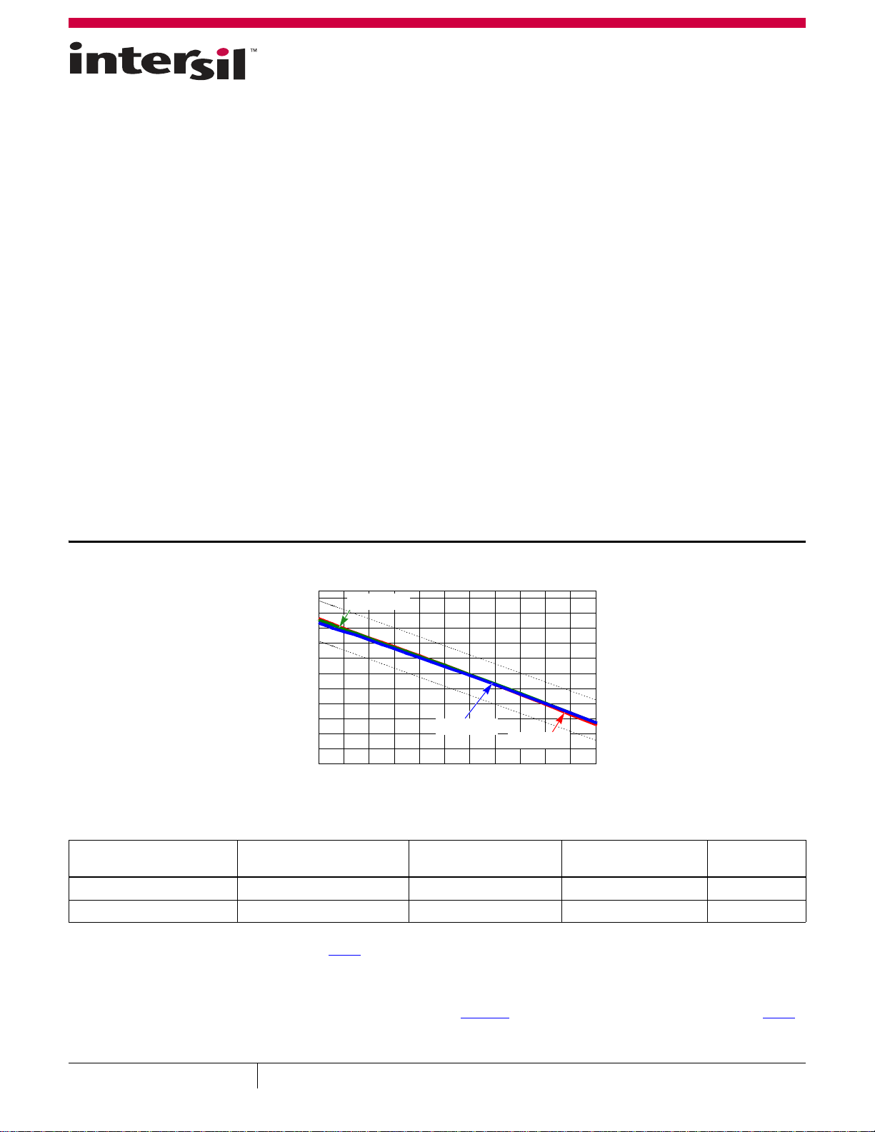
Load Line Regulation
0.91
0.90
0.89
0.88
0.87
0.86
(V)
0.85
OUT
V
0.84
0.83
0.82
0.81
0.80
VIN = 19V
0 6 12 18 24
Features
•Serial Data Bus
•Dual Outputs:
- Configurable 3-, 2- or 1-phase for the 1st Output using 2
integrated Gate Drivers
- 1-phase for the 2nd Output using an Integrated Gate
Driver
• 0.5% System Accuracy Over-Temperature
• Supports Multiple Current Sensing Methods
- Lossless Inductor DCR Current Sensing
- Precision Resistor Current Sensing
• Differential Remote Voltage Sensing
•Programmable V
• Resistor Programmable I
Voltage at Start-up
BOOT
MAX
, T
for Both Outputs
MAX
• Adaptive Body Diode Conduction Time Reduction
Applications
• IMVP-7/VR12 Compliant Computers
VIN = 12V
VIN = 8V
30 36 42 48 54 60 66
(A)
I
OUT
Ordering Information
PART NUMBER
(Notes 1, 2, 3) PART MARKING
ISL95831HRTZ 95831 HRTZ -10 to +100 48 Ld 6x6 TQFN L48.6x6
ISL95831IRTZ 95831 IRTZ -40 to +100 48 Ld 6x6 TQFN L48.6x6
NOTES:
1. Add “-T*” suffix for tape and reel. Please refer to TB347
2. These Intersil Pb-free plastic packaged products employ special Pb-free material sets, molding compounds/die attach materials, and 100% matte
tin plate plus anneal (e3 termination finish, which is RoHS compliant and compatible with both SnPb and Pb-free soldering operations). Intersil Pbfree products are MSL classified at Pb-free peak reflow temperatures that meet or exceed the Pb-free requirements of IPC/JEDEC J STD-020.
3. For Moisture Sensitivity Level (MSL), please see device information page for ISL95831
January 21, 2011
FN7613.0
1
for details on reel specifications.
CAUTION: These devices are sensitive to electrostatic discharge; follow proper IC Handling Procedures.
1-888-INTERSIL or 1-888-468-3774
TEMP. RANGE
(°C)
. For more information on MSL please see techbrief TB363.
Intersil (and design) is a trademark owned by Intersil Corporation or one of its subsidiaries.
All other trademarks mentioned are the property of their respective owners.
|Copyright Intersil Americas Inc. 2011. All Rights Reserved
PACKAGE
(Pb-Free)
PKG.
DWG. #
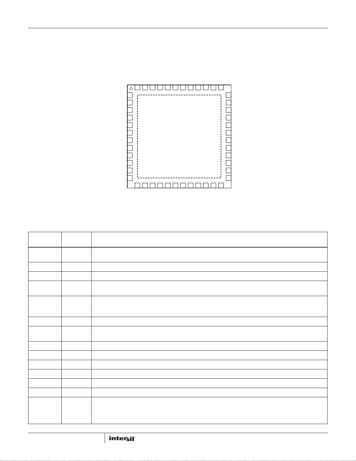
Pin Configuration
VWG
IMONG
PGOODG
SDA
ALERT#
SCLK
VR_ON
PGOOD
IMON
VR_HOT#
NTC
VW
ISL95831
ISL95831
(48 LD TQFN)
TOP VIEW
RTNG
ISUMPG
GND PAD
(BOTTOM)
ISEN2
ISEN1
ISUMNG
VSEN
NTCG
RTN
FBG
COMPG
48 47 46 45 44 43 42 41 40 39
1
2
3
4
5
6
7
8
9
10
11
12
13 14 15 16 17 18 19 20 21 22
VSENG
FB
COMP
ISEN3/FB2
PROG2
BOOTG
UGATEGVDD
PHASEG
LGATEG
38 37
36
BOOT2
35
UGATE2
PHASE2
34
VSSP2
33
32
LGATE2
VCCP
31
30
PWM3
29
LGATE1
VSSP1
28
PHASE1
27
UGATE1
26
25
BOOT1
23 24
VIN
ISUMP
ISUMN
PROG1
Pin Descriptions
ISL95831
PIN NUMBER SYMBOL DESCRIPTION
BOTTOM PAD GND Signal common of the IC. Unless otherwise stated, signals are referenced to the GND pin. It should also be used as the
thermal pad for heat removal.
1 VWG A resistor from this pin to COMPG programs the switching frequency for VR2 (8kΩ gives approximately 300kHz).
2 IMONG An analog output. IMONG outputs a current proportional to VR2 output current.
3 PGOODG Power-Good open-drain output indicating when VR2 is able to supply regulated voltage. Pull up externally with a 680Ω
4, 5, 6 SDA,
ALERT#,
SCLK
7 VR_ON Controller enable input. A high level logic signal on this pin enables the controller.
8 PGOOD Power-Good open-drain output indicating when VR1 is able to supply regulated voltage. Pull up externally with a 680Ω
9 IMON An analog output. IMON outputs a current proportional to VR1 output current.
10 VR_HOT# Open drain thermal overload output indicator. Can be considered part of communication bus with CPU.
11 NTC One of the thermistor inputs to VR_HOT# circuit. Use it to monitor VR1 temperature.
12 VW A resistor from this pin to COMP programs the switching frequency for VR1 (8kΩ gives approximately 300kHz).
13 COMP This pin is the output of the error amplifier for VR1.
14 FB This pin is the inverting input of the error amplifier for VR1.
15 ISEN3/FB2 When the VR1 is configured in 3-phase mode, this pin is ISEN3. ISEN3 is the individual current sensing for VR1 phase 3.
resistor to VCCP or 1.9kΩ to 3.3V.
Communication bus between the CPU and the VRs.
resistor to VCCP or 1.9kΩ to 3.3V.
When VR1 is configured in 2-phase mode, this pin is FB2. There is a switch between the FB2 pin and the FB pin. The
switch is on when VR1 is in 2-phase mode and is off in 1-phase mode. The components connecting to FB2 are used to
adjust the compensation in 1-phase mode to achieve optimum performance for VR1.
2
FN7613.0
January 21, 2011
ISL95831
Pin Descriptions (Continued)
ISL95831
PIN NUMBER SYMBOL DESCRIPTION
16 ISEN2 Individual current sensing for VR1 Phase 2. When ISEN2 and PWM3 are both pulled to 5V VDD, the controller will
disable VR1 Phases 3 and 2.
17 ISEN1 Individual current sensing for VR1 Phase 1.
18 VSEN VR1 remote voltage sense input.
19 RTN VR1 remote voltage sense return.
20, 21 ISUMN and
ISUMP
22 VDD 5V bias power.
23 VIN This pin is connected to the power stage input voltage and used for feed-forward.
24 PROG1 A resistor from this pin to GND programs Imax for VR1, and V
25 BOOT1 Connect an MLCC capacitor across the BOOT1 and the PHASE1 pins. The boot capacitor is charged through an internal
26 UGATE1 Output of VR1 Phase-1 high-side MOSFET gate driver. Connect the UGATE1 pin to the gate of the Phase-1 high-side
27 PHASE1 Current return path for the VR1 Phase-1 high-side MOSFET gate driver. Connect the PHASE1 pin to the node consisting
28 VSSP1 Current return path for VR1 Phase-1 low-side MOSFET gate driver. Connect the VSSP1 pin to the source of VR1 Phase-
29 LGATE1 Output of VR1 Phase-1 low-side MOSFET gate driver. Connect the LGATE1 pin to the gate of VR1 Phase-1 low-side
30 PWM3 PWM output for VR1 Phase 3. When PWM3 is pulled to 5V VDD, the controller will disable VR1 Phase 3.
31 VCCP Input voltage bias for the internal gate drivers. Connect +5V to the VCCP pin. Decouple with at least 1µF of an MLCC
32 LGATE2 Output of VR1 Phase-2 low-side MOSFET gate driver. Connect the LGATE2 pin to the gate of VR1 Phase-2 low-side
33 VSSP2 Current return path for VR1 Phase-2 low-side MOSFET gate driver. Connect the VSSP2 pin to the source of VR1 Phase-2
34 PHASE2 Current return path for VR1 Phase-2 high-side MOSFET gate driver. Connect the PHASE2 pin to the node consisting of
35 UGATE2 Output of VR1 Phase-2 high-side MOSFET gate driver. Connect the UGATE2 pin to the gate of VR1 Phase-2 high-side
36 BOOT2 Connect an MLCC capacitor across the BOOT2 and the PHASE2 pins. The boot capacitor is charged through an internal
37 LGATEG Output of VR2 low-side MOSFET gate driver. Connect the LGATEG pin to the gate of VR2 low-side MOSFET.
38 PHASEG Current return path for VR2 high-side MOSFET gate driver. Connect the PHASEG pin to the node consisting of the
39 UGATEG Output of VR2 high-side MOSFET gate driver. Connect the UGATEG pin to the gate of VR2 high-side MOSFET.
40 BOOTG Connect an MLCC capacitor across the BOOTG and the PHASEG pins. The boot capacitor is charged through an internal
41 PROG2 A resistor from this pin to GND programs I
42 NTCG The second thermistor input to VR_HOT# circuit. Use it to monitor VR2 temperature.
VR1 droop current sense input.
for both VR1 and VR2.
BOOT
boot diode connected from the VCCP pin to the BOOT1 pin, each time the PHASE1 pin drops below VCCP minus the
voltage dropped across the internal boot diode.
MOSFET.
of the high-side MOSFET source, the low-side MOSFET drain, and the output inductor of VR1 Phase 1.
1 low-side MOSFET through a low impedance path, preferably in parallel with the traces connecting the LGATE1 pin to
the gates of the Phase-1 low-side MOSFET.
MOSFET.
capacitor.
MOSFET.
low-side MOSFET through a low impedance path, preferably in parallel with the traces connecting the LGATE2 pin to
the gates of the Phase-2 low-side MOSFET.
the high-side MOSFET source, the low-side MOSFET drain, and the output inductor of VR1 Phase 2.
MOSFET.
boot diode connected from the VCCP pin to the BOOT2 pin, each time the PHASE2 pin drops below VCCP minus the
voltage dropped across the internal boot diode.
high-side MOSFET source, the low-side MOSFET drain, and the output inductor of VR2.
boot diode connected from the VCCP pin to the BOOTG pin, each time the PHASEG pin drops below VCCP minus the
voltage dropped across the internal boot diode.
for VR2 and T
MAX
for both VR1 and VR2.
MAX
3
FN7613.0
January 21, 2011
ISL95831
Pin Descriptions (Continued)
ISL95831
PIN NUMBER SYMBOL DESCRIPTION
43, 44 ISUMNG and
ISUMPG
45 RTNG VR2 remote voltage sense return.
46 VSENG VR2 remote voltage sense input.
47 FBG This pin is the inverting input of the error amplifier for VR2.
48 COMPG This pin is the output of the error amplifier for VR2. Also, a resistor from COMPG to GND can program the operational
VR2 droop current sense input. When ISUMNG is pulled to 5V VDD, VR2 is disabled and all communication to VR2 is
rejected.
modes of VR2.
4
FN7613.0
January 21, 2011
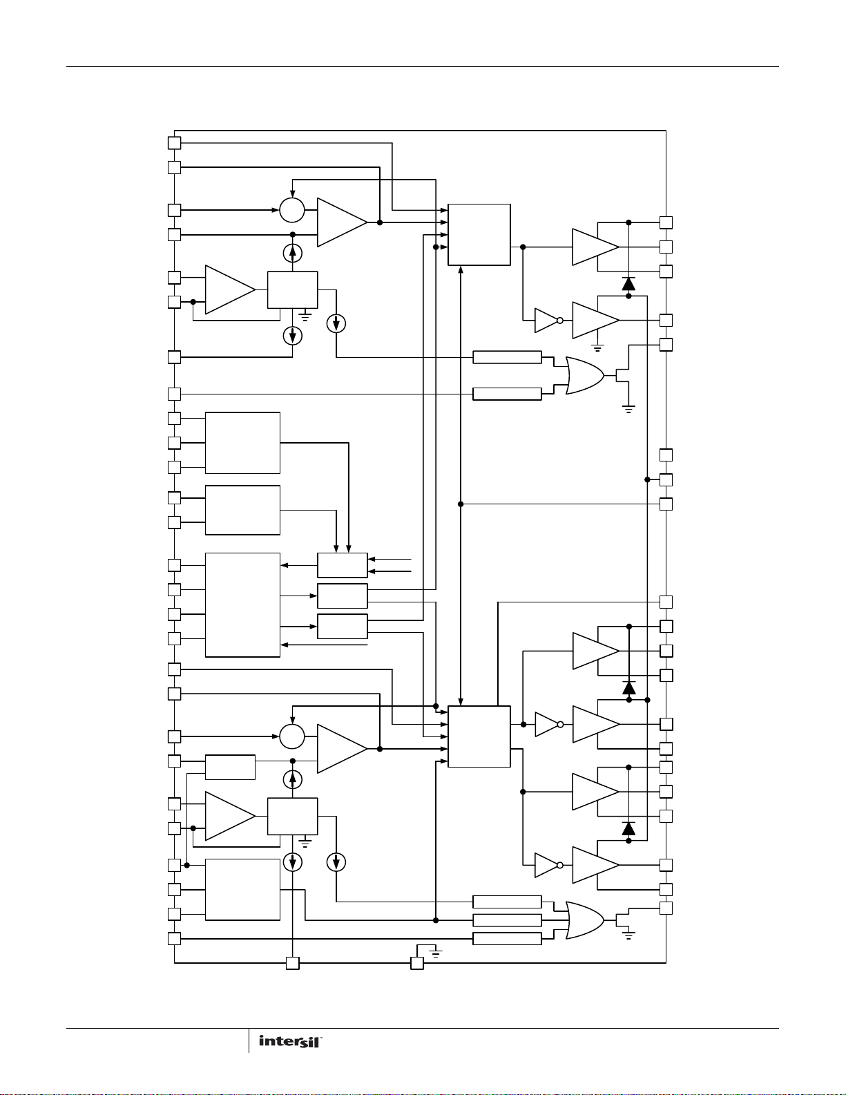
Block Diagram
VWG
COMPG
RTNG
FBG
ISUMPG
ISUMNG
ISL95831
+
+
+
_
CURRENT
SENSE
Σ
+
E/A
_
IDROOPG
VR2
MODULATOR
DRIVER
DRIVER
BOOTG
UGATEG
PHASEG
LGATEG
IMONG
VSENG
NTCG
NTC
VR_HOT#
PROG2
PROG1
VR_ON
SDA
ALERT#
SCLK
VW
COMP
RTN
FB
ISUMP
ISUMN
TEMP
MONITOR
IMAX
VBOOT
TMAX
SET (A/D)
DIGITAL
INTERFACE
FB2
CIRCUIT
+
_
T_MONITOR
PROG
+
+
Σ
CURRENT
SENSE
MODE
+
E/A
_
IDROOP
IMONG
A/D IMON
DAC2
DAC1
D/A
MODE2
MODE1
VREADY
OC FAULT
OV FAULT
VR1
MODULATOR
DRIVER
DRIVER
DRIVER
PGOODG
VDD
VCCP
VIN
PWM3
BOOT2
UGATE2
PHASE2
LGATE2
VSSP2
BOOT1
UGATE1
PHASE1
ISEN3/FB2
ISEN2
ISEN1
VSEN
CURRENT
BALANCING
5
DRIVER
OC FAULT
IBAL FAULT
OV FAULT
GNDIMON
LGATE1
VSSP1
PGOOD
January 21, 2011
FN7613.0
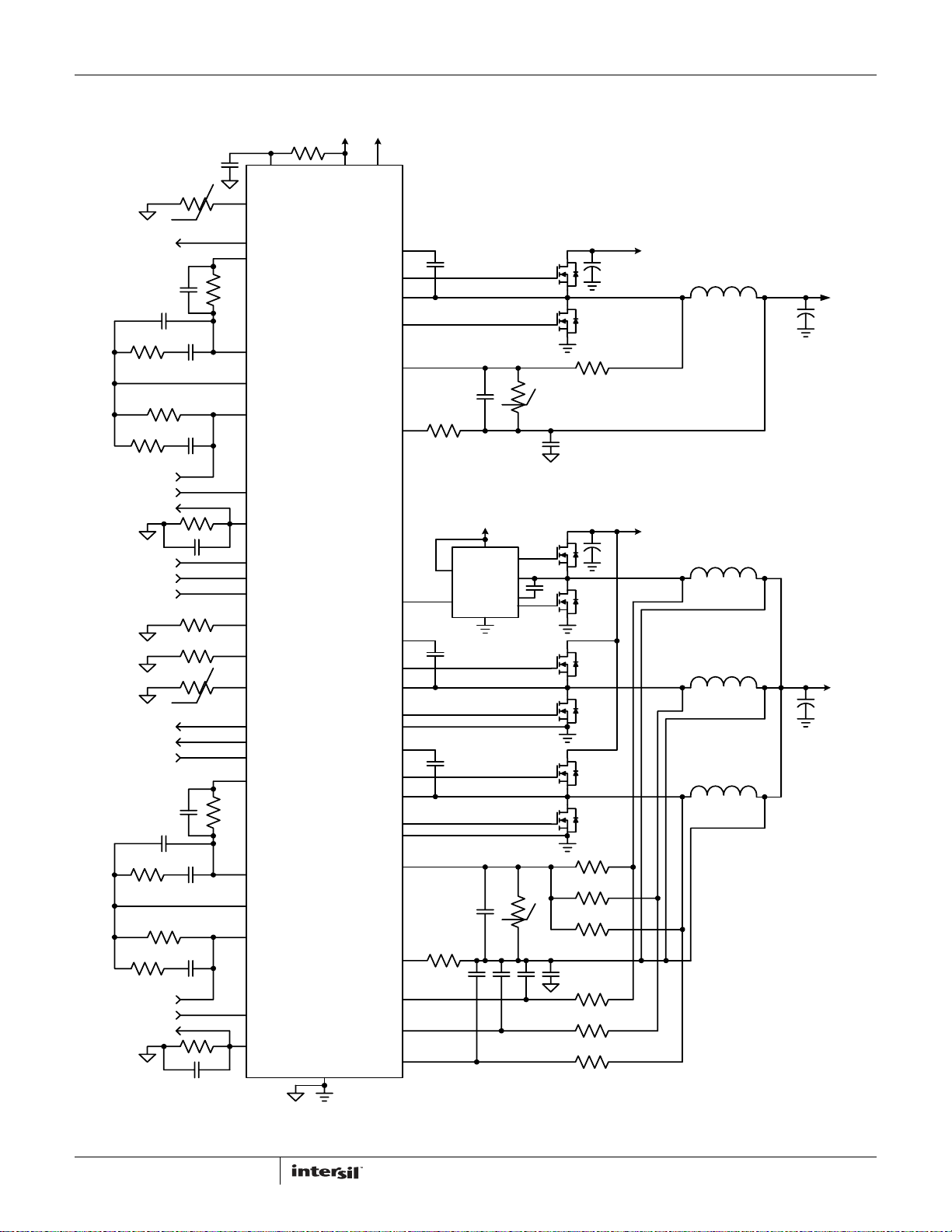
Simplified Application Circuit
V+5
ISL95831
VIN
Rntcg
°c
PGOODG PGOODG
Rdroopg
VCCSENSEG
VSSSENSEG
IMONG
SDA SDA
ALERT# ALERT#
SCLK SCLK
Rprog2
Rprog1
Rntc
°c
VR_HOT# VR_HOT#
PGOOD
VR_ON
Rdroop
VCCSENSE
VSSSENSE
IMON
NTCG
VWG
Rfsetg
COMPG
FBG
VSENG
RTNG
IMONG
PROG2
PROG1
NTC
PGOOD
VR_ON
VW
Rfset
COMP
FB
VSEN
RTN
IMON
VDD
ISL95831
GND
PVCC
VIN
BOOTG
UGATEG
PHASEG
LGATEG
ISUMPG
ISUMNG
PWM3
BOOT2
UGATE2
PHASE2
LGATE2
VSSP2
BOOT1
UGATE1
PHASE1
LGATE1
VSSP1
ISUMP
ISUMN
ISEN3/FB2
ISEN2
ISEN1
Rig
Ri
Cng
FCCM
ISL6208
PWM
Cn
V+5
VCC
GND
°c
UGATE
PHASE
BOOT
LGATE
°c
Cisen3Cisen2Cisen1
Rng
Vsumng
Rn
Cvsumng
Vsumn
Cvsumv
Rsum4
Rsum3
Rsum2
Rsum1
Risen3
Risen2
Risen1
Vin
Vin
L4
L3
L2
L1
AXG Vcore
CPU Vcore
FIGURE 1. TYPICAL ISL95831 APPLICATION CIRCUIT USING INDUCTOR DCR SENSING
6
FN7613.0
January 21, 2011
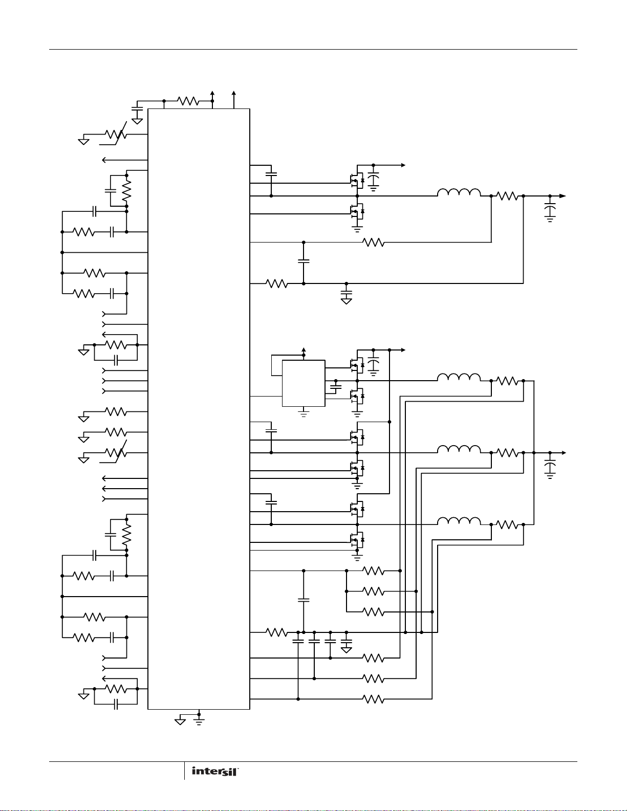
Simplified Application Circuit
V+5
VIN
PVCC
VDD
Rntcg
°C
NTCG
VIN
ISL95831
PGOODG PGOODG
Rfsetg
Rdroopg
VCCSENSEG
VSSSENSEG
IMONG
SDA SDA
ALERT# ALERT#
SCLK SCLK
Rprog2
Rprog1
Rntc
°C
VR_HOT# VR_HOT#
PGOOD
VR_ON
Rfset
Rdroop
VCCSENSE
VSSSENSE
IMON
VWG
COMPG
FBG
VSENG
RTNG
IMONG
PROG2
PROG1
NTC
PGOOD
VR_ON
VW
COMP
FB
VSEN
RTN
IMON
ISL95831
GND
BOOTG
UGATEG
PHASEG
LGATEG
ISUMPG
ISUMNG
PWM3
BOOT2
UGATE2
PHASE2
LGATE2
VSSP2
BOOT1
UGATE1
PHASE1
LGATE1
VSSP1
ISUMP
ISUMN
ISEN3/FB2
ISEN2
ISEN1
Vin
L4
Rsum4
Cng
Rig
V+5
VCC
FCCM
ISL6208
PWM
GND
Cn
Ri
UGATE
PHASE
BOOT
LGATE
Cisen3Cisen2Cisen1
Vsumng
Cvsumng
Vin
L3
L2
L1
Rsum3
Rsum2
Rsum1
Vsumn
Cvsumn
Risen3
Risen2
Risen1
Rsen4
Rsen3
Rsen2
Rsen1
AXG Vcore
CPU Vcore
FIGURE 2. TYPICAL ISL95831 APPLICATION CIRCUIT USING RESISTOR SENSING
7
FN7613.0
January 21, 2011

ISL95831
Table of Contents
Load Line Regulation . . . . . . . . . . . . . . . . . . . . . . . . . . . . . . . . . . . . . . . . . . . . . . . . . . . . . . . . . . . . . . . . . . . . . . . . . . . . . . . . . . . . 1
Pin Descriptions. . . . . . . . . . . . . . . . . . . . . . . . . . . . . . . . . . . . . . . . . . . . . . . . . . . . . . . . . . . . . . . . . . . . . . . . . . . . . . . . . . . . . . . . . 2
Block Diagram . . . . . . . . . . . . . . . . . . . . . . . . . . . . . . . . . . . . . . . . . . . . . . . . . . . . . . . . . . . . . . . . . . . . . . . . . . . . . . . . . . . . . . . . . . 5
Simplified Application Circuit . . . . . . . . . . . . . . . . . . . . . . . . . . . . . . . . . . . . . . . . . . . . . . . . . . . . . . . . . . . . . . . . . . . . . . . . . . . 6
Simplified Application Circuit . . . . . . . . . . . . . . . . . . . . . . . . . . . . . . . . . . . . . . . . . . . . . . . . . . . . . . . . . . . . . . . . . . . . . . . . . . . 7
Absolute Maximum Ratings . . . . . . . . . . . . . . . . . . . . . . . . . . . . . . . . . . . . . . . . . . . . . . . . . . . . . . . . . . . . . . . . . . . . . . . . . . . . . . . 9
Thermal Information . . . . . . . . . . . . . . . . . . . . . . . . . . . . . . . . . . . . . . . . . . . . . . . . . . . . . . . . . . . . . . . . . . . . . . . . . . . . . . . . . . . . . 9
Recommended Operating Conditions. . . . . . . . . . . . . . . . . . . . . . . . . . . . . . . . . . . . . . . . . . . . . . . . . . . . . . . . . . . . . . . . . . . . . . . 9
Gate Driver Timing Diagram. . . . . . . . . . . . . . . . . . . . . . . . . . . . . . . . . . . . . . . . . . . . . . . . . . . . . . . . . . . . . . . . . . . . . . . . . . . . . . 12
Theory of Operation . . . . . . . . . . . . . . . . . . . . . . . . . . . . . . . . . . . . . . . . . . . . . . . . . . . . . . . . . . . . . . . . . . . . . . . . . . . . . . . . . . . . 12
Multiphase R3™ Modulator. . . . . . . . . . . . . . . . . . . . . . . . . . . . . . . . . . . . . . . . . . . . . . . . . . . . . . . . . . . . . . . . . . . . . . . . . . . . 12
Diode Emulation and Period Stretching . . . . . . . . . . . . . . . . . . . . . . . . . . . . . . . . . . . . . . . . . . . . . . . . . . . . . . . . . . . . . . . . . 13
Start-up Timing . . . . . . . . . . . . . . . . . . . . . . . . . . . . . . . . . . . . . . . . . . . . . . . . . . . . . . . . . . . . . . . . . . . . . . . . . . . . . . . . . . . . . . 14
Voltage Regulation and Load Line Implementation . . . . . . . . . . . . . . . . . . . . . . . . . . . . . . . . . . . . . . . . . . . . . . . . . . . . . . . 14
Differential Voltage Sensing . . . . . . . . . . . . . . . . . . . . . . . . . . . . . . . . . . . . . . . . . . . . . . . . . . . . . . . . . . . . . . . . . . . . . . . . . . . 18
Phase Current Balancing . . . . . . . . . . . . . . . . . . . . . . . . . . . . . . . . . . . . . . . . . . . . . . . . . . . . . . . . . . . . . . . . . . . . . . . . . . . . . . 18
CCM Switching Frequency . . . . . . . . . . . . . . . . . . . . . . . . . . . . . . . . . . . . . . . . . . . . . . . . . . . . . . . . . . . . . . . . . . . . . . . . . . . . . 20
Modes of Operation . . . . . . . . . . . . . . . . . . . . . . . . . . . . . . . . . . . . . . . . . . . . . . . . . . . . . . . . . . . . . . . . . . . . . . . . . . . . . . . . . . .20
Dynamic Operation. . . . . . . . . . . . . . . . . . . . . . . . . . . . . . . . . . . . . . . . . . . . . . . . . . . . . . . . . . . . . . . . . . . . . . . . . . . . . . . . . . . 21
VR_HOT#/ALERT# Behavior . . . . . . . . . . . . . . . . . . . . . . . . . . . . . . . . . . . . . . . . . . . . . . . . . . . . . . . . . . . . . . . . . . . . . . . . . . . 21
Current Monitor. . . . . . . . . . . . . . . . . . . . . . . . . . . . . . . . . . . . . . . . . . . . . . . . . . . . . . . . . . . . . . . . . . . . . . . . . . . . . . . . . . . . . . 22
FB2 Function . . . . . . . . . . . . . . . . . . . . . . . . . . . . . . . . . . . . . . . . . . . . . . . . . . . . . . . . . . . . . . . . . . . . . . . . . . . . . . . . . . . . . . . . 22
Adaptive Body Diode Conduction Time Reduction . . . . . . . . . . . . . . . . . . . . . . . . . . . . . . . . . . . . . . . . . . . . . . . . . . . . . . . . .22
Protections . . . . . . . . . . . . . . . . . . . . . . . . . . . . . . . . . . . . . . . . . . . . . . . . . . . . . . . . . . . . . . . . . . . . . . . . . . . . . . . . . . . . . . . . . .23
Supported Data And Configuration Registers. . . . . . . . . . . . . . . . . . . . . . . . . . . . . . . . . . . . . . . . . . . . . . . . . . . . . . . . . . . . . 23
Key Component Selection . . . . . . . . . . . . . . . . . . . . . . . . . . . . . . . . . . . . . . . . . . . . . . . . . . . . . . . . . . . . . . . . . . . . . . . . . . . . . . . 24
Inductor DCR Current-Sensing Network . . . . . . . . . . . . . . . . . . . . . . . . . . . . . . . . . . . . . . . . . . . . . . . . . . . . . . . . . . . . . . . . . 24
Resistor Current-Sensing Network . . . . . . . . . . . . . . . . . . . . . . . . . . . . . . . . . . . . . . . . . . . . . . . . . . . . . . . . . . . . . . . . . . . . . 26
Overcurrent Protection . . . . . . . . . . . . . . . . . . . . . . . . . . . . . . . . . . . . . . . . . . . . . . . . . . . . . . . . . . . . . . . . . . . . . . . . . . . . . . . .26
Compensator. . . . . . . . . . . . . . . . . . . . . . . . . . . . . . . . . . . . . . . . . . . . . . . . . . . . . . . . . . . . . . . . . . . . . . . . . . . . . . . . . . . . . . . . 27
Programming Resistors . . . . . . . . . . . . . . . . . . . . . . . . . . . . . . . . . . . . . . . . . . . . . . . . . . . . . . . . . . . . . . . . . . . . . . . . . . . . . . .30
Current Monitor . . . . . . . . . . . . . . . . . . . . . . . . . . . . . . . . . . . . . . . . . . . . . . . . . . . . . . . . . . . . . . . . . . . . . . . . . . . . . . . . . . . . . .30
Current Balancing . . . . . . . . . . . . . . . . . . . . . . . . . . . . . . . . . . . . . . . . . . . . . . . . . . . . . . . . . . . . . . . . . . . . . . . . . . . . . . . . . . . .30
Slew Rate Compensation Circuit For VID Transition . . . . . . . . . . . . . . . . . . . . . . . . . . . . . . . . . . . . . . . . . . . . . . . . . . . . . . . .31
Layout Guidelines . . . . . . . . . . . . . . . . . . . . . . . . . . . . . . . . . . . . . . . . . . . . . . . . . . . . . . . . . . . . . . . . . . . . . . . . . . . . . . . . . . . . . . 35
Typical Performance . . . . . . . . . . . . . . . . . . . . . . . . . . . . . . . . . . . . . . . . . . . . . . . . . . . . . . . . . . . . . . . . . . . . . . . . . . . . . . . . . . . . 37
Revision History . . . . . . . . . . . . . . . . . . . . . . . . . . . . . . . . . . . . . . . . . . . . . . . . . . . . . . . . . . . . . . . . . . . . . . . . . . . . . . . . . . . . . . . 41
Products . . . . . . . . . . . . . . . . . . . . . . . . . . . . . . . . . . . . . . . . . . . . . . . . . . . . . . . . . . . . . . . . . . . . . . . . . . . . . . . . . . . . . . . . . . . . . . 41
Package Outline Drawing . . . . . . . . . . . . . . . . . . . . . . . . . . . . . . . . . . . . . . . . . . . . . . . . . . . . . . . . . . . . . . . . . . . . . . . . . . . . . . . 42
8
FN7613.0
January 21, 2011
ISL95831
Absolute Maximum Ratings Thermal Information
Supply Voltage, VDD. . . . . . . . . . . . . . . . . . . . . . . . . . . . . . . . . . . -0.3V to +7V
Battery Voltage, VIN . . . . . . . . . . . . . . . . . . . . . . . . . . . . . . . . . . . . . . . . . +28V
Boot Voltage (BOOT). . . . . . . . . . . . . . . . . . . . . . . . . . . . . . . . . . -0.3V to +33V
Boot-to-Phase Voltage
(BOOT-PHASE) -0.3V to +7V(DC) . . . . . . . . . . . . . . -0.3V to +9V(<10ns)
Phase Voltage (PHASE) . . . . . . . . . . . . . . . . -7V (<20ns Pulse Width, 10µJ)
UGATE Voltage (UGATE) . . . . . . . . . . . . . . . . . . . PHASE - 0.3V (DC) to BOOT
. . . . . . . . . . . . . . . . . . . . PHASE - 5V (<20ns Pulse Width, 10µJ) to BOOT
LGATE Voltage
. . . . . . . . . . . . . . . . . . . . . . . . -2.5V (<20ns Pulse Width, 5µJ) to VDD+0.3V
All Other Pins . . . . . . . . . . . . . . . . . . . . . . . . . . . . . . . . . -0.3V to (VDD +0.3V)
Open Drain Outputs, PGOOD, VR_HOT#, ALERT#. . . . . . . . . . -0.3V to +7V
ESD Rating
Human Body Model (Tested per JESD22-A114E). . . . . . . . . . . . . . . . 2kV
Machine Model (Tested per JESD22-A115-A) . . . . . . . . . . . . . . . . . 200V
Charged Device Model (Tested per JESD22-C101A) . . . . . . . . . . . . . . 1k
Latch Up (Tested per JESD-78B; Class 2, Level A) . . . . . . . . . . . . . . 100mA
CAUTION: Do not operate at or near the maximum ratings listed for extended periods of time. Exposure to such conditions may adversely impact product
reliability and result in failures not covered by warranty.
NOTES:
4. θ
is measured in free air with the component mounted on a high effective thermal conductivity test board with “direct attach” features. See Tech
JA
Brief TB379.
5. For θ
, the “case temp” location is the center of the exposed metal pad on the package underside.
JC
Thermal Resistance (Typical) θ
48 Ld TQFN Package (Notes 4, 5) . . . . . . . 29 1
Maximum Junction Temperature . . . . . . . . . . . . . . . . . . . . . . . . . . . .+150°C
Maximum Storage Temperature Range . . . . . . . . . . . . . .-65°C to +150°C
Maximum Junction Temperature (Plastic Package) . . . . . . . . . . . .+150°C
Storage Temperature Range. . . . . . . . . . . . . . . . . . . . . . . .-65°C to +150°C
Pb-Free Reflow Profile . . . . . . . . . . . . . . . . . . . . . . . . . . . . . . . see link below
http://www.intersil.com/pbfree/Pb-FreeReflow.asp
(°C/W) θJC (°C/W)
JA
Recommended Operating Conditions
Supply Voltage, VDD. . . . . . . . . . . . . . . . . . . . . . . . . . . . . . . . . . . . . . +5V ±5%
Battery Voltage, VIN . . . . . . . . . . . . . . . . . . . . . . . . . . . . . . . . . . +4.5V to 25V
Ambient Temperature
HRTZ. . . . . . . . . . . . . . . . . . . . . . . . . . . . . . . . . . . . . . . . . . -10°C to +100°C
IRTZ . . . . . . . . . . . . . . . . . . . . . . . . . . . . . . . . . . . . . . . . . .-40°C to +100°C
Junction Temperature
HRTZ. . . . . . . . . . . . . . . . . . . . . . . . . . . . . . . . . . . . . . . . . .-10°C to +125°C
IRTZ . . . . . . . . . . . . . . . . . . . . . . . . . . . . . . . . . . . . . . . . . .-40°C to +125°C
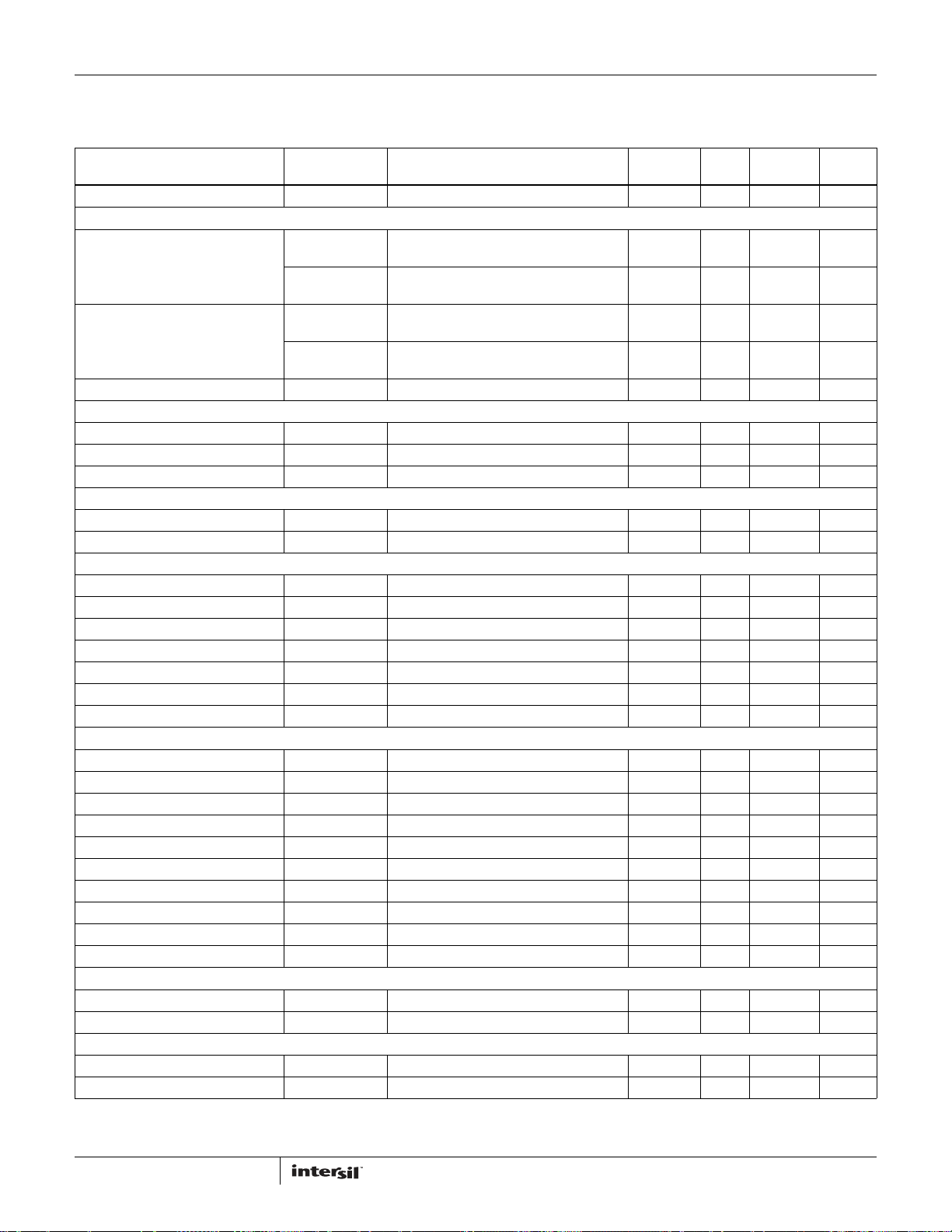
Electrical Specifications "Operating Conditions: VDD = 5V, T
(ISL95831HRTZ), fSW = 300kHz, unless otherwise noted." Boldface limits apply over the operating temperature ranges, -10°C to +100°C or
= -40°C to +100°C (ISL95831IRTZ), TA = -10°C to +100°C
A
-40°C to +100°C.
PARAMETER SYMBOL TEST CONDITIONS
MIN
(Note 6) TYP
MAX
(Note 6) UNITS
INPUT POWER SUPPLY
+5V Supply Current I
Battery Supply Current I
Input Resistance R
V
IN
VDD
VIN
VIN
VR_ON = 1V 9.2 10.5 mA
VR_ON = 0V 1 µA
VR_ON = 0V 1 µA
VR_ON = 1V 550 kΩ
POWER-ON-RESET THRESHOLDS
VDD Power-On-Reset Threshold VDDPOR
VDDPOR
VIN Power-On-Reset Threshold VINPOR
VINPOR
VDD rising 4.35 4.5 V
r
VDD falling 4.00 4.15 V
f
VIN rising 4.00 4.35 V
r
VIN falling 2.8 3.3 V
f
SYSTEM AND REFERENCES
System Accuracy HRTZ
%Error (V
IRTZ
%Error (V
Internal V
Maximum Output Voltage V
BOOT
OUT(max)
No load; closed loop, active mode range,
VID = 0.75V to 1.52V, -0.5 +0.5 %
OUT)
VID = 0.5V to 0.745V -8 +8 mV
VID = 0.25V to 0.495V -15 +15 mV
No load; closed loop, active mode range,
)
VID = 0.75V to 1.52V -0.8 +0.8 %
OUT
VID = 0.5V to 0.745V -10 +10 mV
VID = 0.25V to 0.495V -18 +18 mV
HRTZ 1.0945 1.100 1.1055 V
IRTZ 1.0912 1.100 1.1088 V
VID = [11111111] 1.52 V
9
FN7613.0
January 21, 2011
ISL95831
Electrical Specifications "Operating Conditions: VDD = 5V, T
(ISL95831HRTZ), fSW = 300kHz, unless otherwise noted." Boldface limits apply over the operating temperature ranges, -10°C to +100°C or
= -40°C to +100°C (ISL95831IRTZ), TA = -10°C to +100°C
A
-40°C to +100°C. (Continued)
PARAMETER SYMBOL TEST CONDITIONS
Minimum Output Voltage V
OUT(min)
MIN
(Note 6) TYP
VID = [00000001] 0.25 V
MAX
(Note 6) UNITS
CHANNEL FREQUENCY
Nominal Channel Frequency-HRTZ HRTZ_VR1
fSW(nom)
HRTZ_VR2
fSW(nom)
Nominal Channel Frequency-IRTZ IRTZ_VR1
fSW(nom)
IRTZ_VR2
fSW(nom)
R
= 8.66kΩ, 2-channel operation,
fset
V
= 1.1V
COMP
= 9.09kΩ, V
R
fset
R
= 8.66kΩ, 2-channel operation,
fset
V
= 1.1V
COMP
= 9.09kΩ, V
R
fset
= 1.1V 285 300 315 kHz
COMP
= 1.1V 280 300 320 kHz
COMP
285 300 315 kHz
280 300 320 kHz
Adjustment Range 200 500 kHz
AMPLIFIERS
Current-Sense Amplifier Input Offset I
Error Amp DC Gain A
v0
Error Amp Gain-Bandwidth Product GBW C
= 0A -0.15 +0.15 mV
FB
90 dB
= 20pF 18 MHz
L
ISEN
Imbalance Voltage Maximum of ISENs - Minimum of ISENs 1 mV
Input Bias Current 20 nA
POWER-GOOD AND PROTECTION MONITORS
I
PGOOD Low Voltage V
PGOOD Leakage Current I
OL
OH
= 4mA 0.15 0.4 V
PGOOD
PGOOD = 3.3V 1 µA
PGOOD Delay tpgd 1.2 ms
ALERT# Low Voltage 7 12 Ω
VR_HOT# Low Voltage 7 12 Ω
ALERT# Leakage Current 1 µA
VR_HOT# Leakage Current 1 µA
GATE DRIVER
UGATE Pull-Up Resistance R
UGATE Source Current I
UGATE Sink Resistance R
UGATE Sink Current I
LGATE Pull-Up Resistance R
LGATE Source Current I
LGATE Sink Resistance R
LGATE Sink Current I
UGATE to LGATE De adt ime t
LGATE to UGATE De adt ime t
UGPU
UGSRC
UGPD
UGSNK
LGPU
LGSRC
LGPD
LGSNK
UGFLGR
LGFUGR
200mA Source Current 1.0 1.5 Ω
UGATE - PHASE = 2.5V 2.0 A
250mA Sink Current 1.0 1.5 Ω
UGATE - PHASE = 2.5V 2.0 A
250mA Source Current 1.0 1.5 Ω
LGATE - VSSP = 2.5V 2.0 A
250mA Sink Current 0.5 0.9 Ω
LGATE - VSSP = 2.5V 4.0 A
UGATE falling to LGATE rising, no load 23 ns
LGATE falling to UGATE rising, no load 28 ns
BOOTSTRAP DIODE
Forward Voltage V
Reverse Leakage I
F
R
PVCC = 5V, IF = 2mA 0.58 V
VR = 25V 0.2 µA
PROTECTION
Overvoltage Threshold OV
H
VSEN rising above setpoint for >1µs 120 155 200 mV
Current Imbalance Threshold One ISEN above another ISEN for >1.2ms 9 mV
10
FN7613.0
January 21, 2011
ISL95831
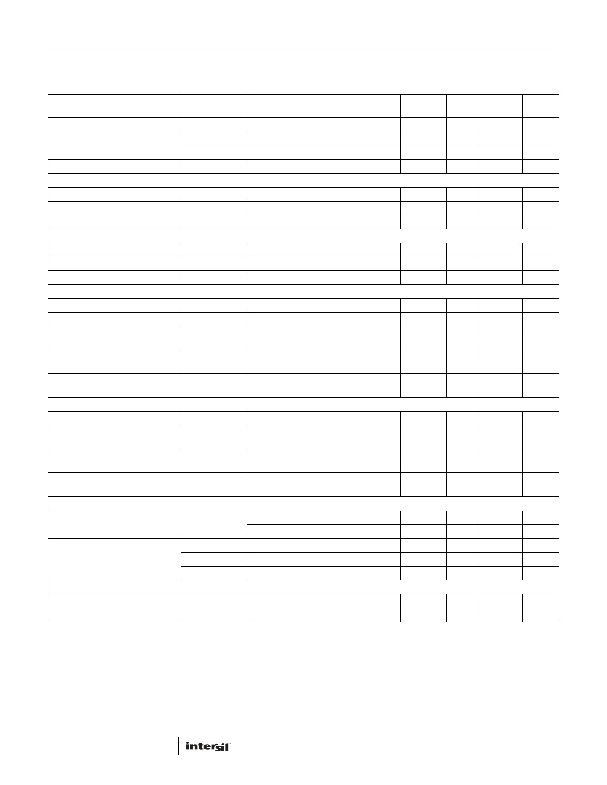
Electrical Specifications "Operating Conditions: VDD = 5V, T
(ISL95831HRTZ), fSW = 300kHz, unless otherwise noted." Boldface limits apply over the operating temperature ranges, -10°C to +100°C or
= -40°C to +100°C (ISL95831IRTZ), TA = -10°C to +100°C
A
-40°C to +100°C. (Continued)
PARAMETER SYMBOL TEST CONDITIONS
VR1 Overcurrent Threshold 3-Phase - PS0 and 1-Phase - all states 25.5 30.6 35.5 µA
3-Phase - PS1, 2-Phase - PS0 16.75 20.6 24.25 µA
3-Phase - PS2, 2-Phase - PS1 and PS2 8.5 10.6 12.75 µA
VR2 Overcurrent Threshold All states 28.5 30.6 33.5 µA
LOGIC THRESHOLDS
VR_ON Input Low V
VR_ON Input High V
PWM
PWM Output Low V
PWM Output High V
PWM Tri-State Leakage PWM = 2.5V 2 µA
THERMAL MONITOR
NTC Source Current NTC = 1.3V 59 60 61 µA
VR_HOT# Trip Voltage (VR1 and VR2) Falling 0.86 0.873 0.89 V
VR_HOT# Reset Voltage (VR1
and VR2)
Therm_Alert Trip Voltage (VR1
and VR2)
Therm_Alert Reset Voltage (VR1
and VR2)
CURRENT MONITOR
IMON Output Current (VR1 and VR2) ISUM- pin current = 25µA 147 150 153 µA
IMON Current Sinking Capability
(VR1 and VR2)
IccMax_Alert Trip Voltage (VR1
and VR2)
IccMax_Alert Reset Voltage (VR1
and VR2)
IL
IH
V
IH
0L
0H
HRTZ 0.7 V
IRTZ 0.75 V
Sinking 5mA 1.0 V
Sourcing 5mA 3.5 4.2 V
Rising 0.905 0.929 0.935 V
Falling 0.9 0.913 0.93 V
Rising 0.945 0.961 0.975 V
Rising 2.63 2.66 2.69 V
Falling 2.585 2.62 2.655 V
MIN
(Note 6) TYP
370 µA
MAX
(Note 6) UNITS
0.3 V
INPUTS
VR_ON Leakage Current I
SCLK, SDA Leakage VR_ON = 0V, SCLK & SDA = 0V & 1V -1 1 µA
SLEW RATE (For VID Change)
Fast Slew Rate 10 mV/µs
Slow Slew Rate 2.5 mV/µs
NOTES:
6. Compliance to datasheet limits is assured by one or more methods: production test, characterization and/or design.
VR_ON
VR_ON = 0V -1 0µA
VR_ON = 1V 18 35 µA
VR_ON = 1V, SCLK & SDA = 1V -5 1 µA
VR_ON = 1V, SCLK & SDA = 0V -85 -60 -30 µA
11
FN7613.0
January 21, 2011

Gate Driver Timing Diagram
PWM
t
LGFUGR
UGATE
t
RU
ISL95831
t
FU
1V
LGATE
t
FL
1V
Theory of Operation
Multiphase R3™ Modulator
MASTER CLOCK CIRCUIT
gmVo
Crs1
Crs2
Crs3
MASTER
CLOCK
Vcrs1
Vcrs2
Vcrs3
VW
COMP
Vcrm
Crm
VW
VW
VW
MASTER
CLOCK
SLAVE CIRCUIT 1
Clock1
gm
SLAVE CIRCUIT 2
Clock2
gm
SLAVE CIRCUIT 3
Clock3
gm
S
Q
R
S
Q
R
S
Q
R
Phase
Sequencer
PWM1
PWM2
PWM3
Phase1
Phase2
Phase3
Clock1
Clock2
Clock3
L1
I
L1
L2
I
L2
L3
I
L3
Vo
Co
t
UGFLGR
t
VW
Vcrm
COMP
Master
Clock
Clock1
PWM1
Clock2
PWM2
Clock3
PWM3
FIGURE 4. R
RL
VW
Vcrs3
Vcrs2 V crs1
3
™ MODULATOR OPERATION PRINCIPLES IN
STEADY STATE
Hysteretic
Window
FIGURE 3. R
3
™ MODULATOR CIRCUIT
12
FN7613.0
January 21, 2011
ISL95831
VW
COMP
Vcrm
Master
Clock
Clock1
PWM1
Clock2
PWM2
Clock3
PWM3
VW
Vcrs1
Vcrs3
Vcrs2
FIGURE 5. R
3
™ MODULATOR OPERATION PRINCIPLES IN LOAD
INSERTION RESPONSE
The ISL95831 is a multiphase regulator implementing Intel™
IMVP-7/VR12™ protocol. It has two voltage regulators, VR1 and
VR2, on one chip. VR1 can be programmed for 1-, 2- or 3-phase
operation, and VR2 is dedicated to 1-phase operation. The
following description is based on VR1, but also applies to VR2
because they are based on the same architecture.
3
The ISL95831 uses Intersil patented R
Regulator™) modulator. The R
3
™ modulator combines the best
™ (Robust Ripple
features of fixed frequency PWM and hysteretic PWM while
eliminating many of their shortcomings. Figure 3 conceptually
shows the multiphase R
3
™ modulator circuit, and Figure 4 shows
the operation principles.
Each slave circuit has its own ripple capacitor C
, whose voltage
rs
mimics the inductor ripple current. A gm amplifier converts the
inductor voltage into a current source to charge and discharge
. The slave circuit turns on its PWM pulse upon receiving the
C
rs
clock signal, and the current source charges Crs. When Crs
voltage V
and the current source discharges C
Since the controller works with V
hits VW, the slave circuit turns off the PWM pulse,
Crs
.
rs
, which are large-amplitude
crs
and noise-free synthesized signals, it achieves lower phase jitter
than conventional hysteretic mode and fixed PWM mode
controllers. Unlike conventional hysteretic mode converters, the
ISL95831 uses an error amplifier that allows the controller to
maintain a 0.5% output voltage accuracy.
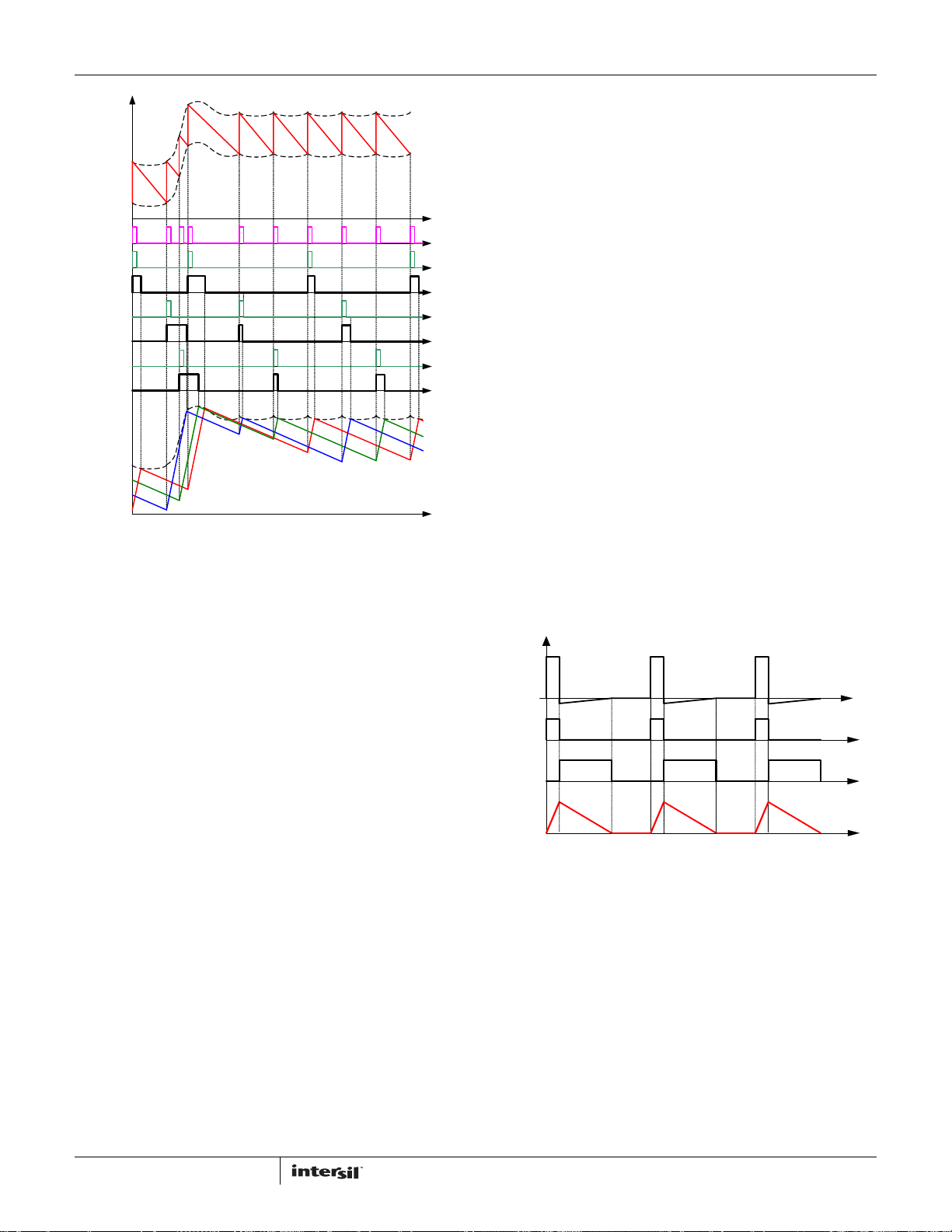
Figure 5 shows the operation principles during load insertion
response. The COMP voltage rises during load insertion,
generating the master clock signal more quickly, so the PWM
pulses turn on earlier, increasing the effective switching
frequency, which allows for higher control loop bandwidth than
conventional fixed frequency PWM controllers. The VW voltage
rises as the COMP voltage rises, making the PWM pulses wider.
During load release response, the COMP voltage falls. It takes
the master clock circuit longer to generate the next master clock
signal so the PWM pulse is held off until needed. The VW voltage
falls as the COMP voltage falls, reducing the current PWM pulse
width. This kind of behavior gives the controller excellent
response speed.
The fact that all the phases share the same VW window voltage
also ensures excellent dynamic current balance among phases.
Diode Emulation and Period Stretching
Phase
UGATE
LGATE
A current source flows from the VW pin to the COMP pin, creating
a voltage window set by the resistor between the two pins. This
voltage window is called VW window in the following discussion.
Inside the IC, the modulator uses the master clock circuit to
generate the clocks for the slave circuits. The modulator
discharges the ripple capacitor C
to g
, where gm is a gain factor. Crm voltage V
mVo
with a current source equal
rm
crm
is a
sawtooth waveform traversing between the VW and COMP
voltages. It resets to VW when it hits COMP, and generates a
one-shot master clock signal. A phase sequencer distributes the
master clock signal to the slave circuits. If VR1 is in 3-phase
mode, the master clock signal will be distributed to the three
phases, and the Clock1~3 signals will be 120° out-of-phase. If
VR1 is in 2-phase mode, the master clock signal will be
distributed to Phases 1 and 2, and the Clock1 and Clock2 signals
will be 180° out-of-phase. If VR1 is in 1-phase mode, the master
clock signal will be distributed to Phases 1 only and be the
Clock1 signal.
13
IL
FIGURE 6. DIODE EMULATION
ISL95831 can operate in diode emulation (DE) mode to improve
light load efficiency. In DE mode, the low-side MOSFET conducts
when the current is flowing from source to drain and doesn’t allow
reverse current, emulating a diode. As Figure 6 shows, when
LGATE is on, the low-side MOSFET carries current, creating
negative voltage on the phase node due to the voltage drop across
the ON-resistance. The controller monitors the current through
monitoring the phase node voltage. It turns off LGATE when the
phase node voltage reaches zero to prevent the inductor current
from reversing the direction and creating unnecessary power loss.
If the load current is light enough, as Figure 6 shows, the inductor
current will reach and stay at zero before the next phase node
pulse and the regulator is in discontinuous conduction mode
(DCM). If the load current is heavy enough, the inductor current
FN7613.0
January 21, 2011
 Loading...