®
www.BDTIC.com/Intersil
ISL95810
Single Digitally Controlled Potentiometer (XDCP™)
Data Sheet September 19, 2006
Low Noise, Low Power I2C Bus, 256 Taps
The ISL95810 integrates a digitally controlled potentiometer
(XDCP) on a monolithic CMOS integrated circuit.
The digitally controlled potentiometer is implemented with a
combination of resistor elements and CMOS switches. The
position of the wiper is controlled by the user through the I
2
C
bus interface. The potentiometer has an associated volatile
Wiper Register (WR) and a non-volatile Initial Value Register
(IVR), that can be directly written to and re ad by th e use r.
The content of the WR controls the position of the wiper. At
power-up the device recalls the contents of the DCP’s IVR to
the WR.
The DCP can be used as three-terminal potentiometer or as
two-terminal variable resistor in a wide variety of applications
including control, parameter adjustments, and signal
processing.
Ordering Information
PART
PART NUMBER
ISL95810WIU8* AIU 10 -40 to +85 8 Ld MSOP
ISL95810WIU8Z
(Note)
ISL95810WIRT8Z*
(Note)
ISL95810UIU8* AIT 50 -40 to +85 8 Ld MSOP
ISL95810UIU8Z*
(Note)
ISL95810UIRT8 AIT -40 to +85 8 Ld 3 x 3 TDFN
ISL95810UIRT8Z*
(Note)
*Add “-T” suffix for tape and reel.
NOTE: Intersil Pb-free plus anneal products employ special Pb-free material
sets; molding compounds/die attach materials and 100% matte tin plate
termination finish, which are RoHS compliant and compatible with both SnPb
and Pb-free soldering operations. Intersil Pb-free products are MSL classified
at Pb-free peak reflow temperatures that meet or exceed the Pb-free
requirements of IPC/JEDEC J STD-020.
MARKING
APN -40 to +85 8 Ld MSOP
APO -40 to +85 8 Ld 3 x 3 TDFN
AOK -40 to +85 8 Ld MSOP
APP -40 to +85 8 Ld 3 x 3 TDFN
R
TOTAL
(kΩ)
TEMP
RANGE (°C) PACKAGE
(Pb-free)
(Pb-free)
(Pb-free)
(Pb-free)
FN8090.2
Features
• 256 resistor taps - 0.4% resoluti o n
2
•I
C serial interface
• Wiper resistance: 70Ω typical @ 3.3V
• Non-volatile storage of wiper position
• Standby current 5µA max
• Power supply: 2.7V to 5.5V
•50kΩ, 10kΩ total resistance
• High reliability
- Endurance: 200,000 data changes per bit per register
- Register data retention: 50 years @ T ≤ +75°C
• 8 Ld MSOP and 8 Ld TDFN packaging
• Pb-free plus anneal available (RoHS compliant)
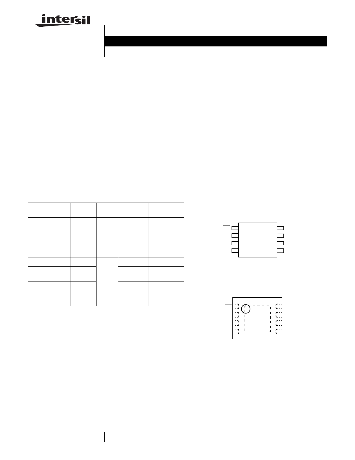
Pinouts
ISL95810
(8 LD MSOP)
TOP VIEW
WP
SCL
SDA
GND
SCL
SDA
GND RW
WP
1
2
3
4
ISL95810
(8 LD TDFN)
TOP VIEW
1
2
3
4
8
V
CC
7
RH
6
RL
RW
5
V
8
CC
7
RH
6
RL
5
1
CAUTION: These devices are sensitive to electrostatic discharge; follow proper IC Handling Procedures.
1-888-INTERSIL or 1-888-468-3774
XDCP is a trademark of Intersil Corporation. Copyright Intersil Americas Inc. 2005, 2006. All Rights Reserved
| Intersil (and design) is a registered trademark of Intersil Americas Inc.
All other trademarks mentioned are the property of their respective owners.

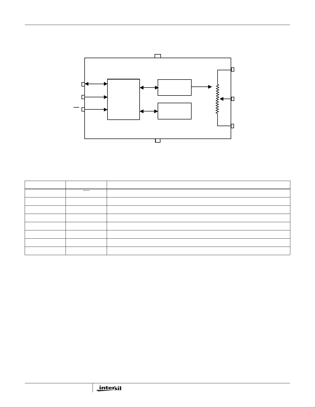
Block Diagram
www.BDTIC.com/Intersil
ISL95810
VCC
RH
SDA
SCL
WP
I2C AND
CONTROL
WIPER
REGISTER
NON-VOLATILE
REGISTER
GND
Pin Descriptions
TSSOP PIN SYMBOL DESCRIPTION
1WPHardware write protection. Active low. Prevents any “Write” operation of the I2C interface.
2
2SCLI
3 SDA Serial data I/O for the I
4 GND Ground
5 RW “Wiper” terminal of the DCP
6 RL “Low” terminal of the DCP
7 RH “High” terminal of the DCP
8V
CC
C interface clock
Power supply
2
C interface
RW
RL
2
FN8090.2
September 19, 2006

ISL95810
www.BDTIC.com/Intersil
Absolute Maximum Ratings Recommended Operating Conditions
Storage Temperature. . . . . . . . . . . . . . . . . . . . . . . .-65°C to +150°C
Voltage at Any Digital Interface Pin
with Respect to V
. . . . . . . . . . . . . . . . . . . . . . . . . . . . . . . . . . . . . . . .-0.3V to +6V
V
CC
Voltage at Any DCP Pin with
Respect to V
. . . . . . . . . . . . . . . . . . . . . . -0.3V to VCC+0.3
SS
. . . . . . . . . . . . . . . . . . . . . . . . . . . . -0.3V to V
SS
CC
Lead Temperature (Soldering, 10s) . . . . . . . . . . . . . . . . . . . .+300°C
I
(10s) . . . . . . . . . . . . . . . . . . . . . . . . . . . . . . . . . . . . . . . . . . ±6mA
W
CAUTION: Stresses above those listed in “Absolute Maximum Ratings” may cause permanent damage to the device. This is a stress only rating and operation of the
device at these or any other conditions above those indicated in the operational sections of this specification is not implied.
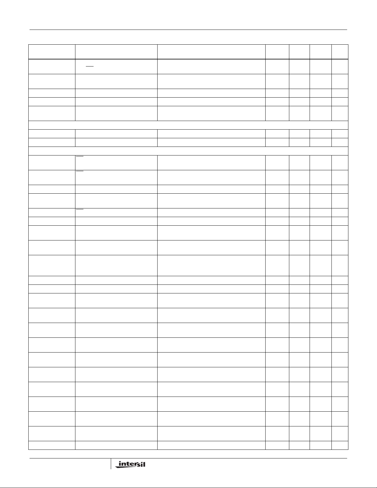
Analog Specifications Over recommended operating conditions unless otherwise stated.
SYMBOL PARAMETER TEST CONDITIONS MIN
R
TOTAL
R
W
C
H/CL/CW
I
LkgDCP
VOLTAGE DIVIDER MODE (0V @ RL; V
(Note 6) Integral Non-Linearity -1 1 LSB (Note 2)
INL
DNL
(Note 5) Differential Non-Linearity Monotonic over all tap positions W option -0.75 -0.75 LSB (Note 2)
RH to RL Resistance W, U versions respectively 10, 50 kΩ
to RL Resistance Tolerance -20 +20 %
R
H
Wiper Resistance VCC = 3.3V @ +25°C
Wiper current = V
Potentiometer Capacitance
(Note 13)
Leakage on DCP Pins (Note 13) Voltage at pin from GND to V
@ RH; measured at RW, unloaded)
CC
ZSerror (Note 3) Zero-Scale Error W option 0 1 7 LSB
U option 0 0.5 2
FSerror
(Note 4) Full-Scale Error W option -7 -1 0 LSB (Note 2)
U option -2 -0.5 0
TC
(Note 7, 13) Ratiometric Temperature
V
Coefficient
DCP Register set to 80 hex ±4 ppm/°C
RESISTOR MODE (Measurements between RW and RL with RH not connected, or between RW and RH with RL not connected)
(Note 11) Integral Non-Linearity DCP register set between 20 hex and FF hex.
RINL
Monotonic over all tap positions
(Note 5) Differential Non-Linearity DCP register set between 20 hex
RDNL
and FF hex. Monotonic over all tap
positions
Roffset
(Note 9) Offset W option 0 1 7 MI (Note 8)
U option 0 0.5 2 MI
TC
R
(Note 12, 13)
Resistance Temperature Coefficient DCP register set between 20 hex and FF hex ±45 ppm/°C
Industrial . . . . . . . . . . . . . . . . . . . . . . . . . . . . . . . . . .-40°C to +85°C
V
. . . . . . . . . . . . . . . . . . . . . . . . . . . . . . . . . . . . . . . . 2.7V to 5.5V
CC
Power Rating of Each DCP . . . . . . . . . . . . . . . . . . . . . . . . . . . .5mW
Wiper Current of Each DCP. . . . . . . . . . . . . . . . . . . . . . . . . .±3.0mA
TYP
(Note 1) MAX UNIT
70 200 Ω
CC/RTOTAL
10/10/25 pF
CC
0.1 1 µA
U option -0.5 -0.5 LSB
-1 1 MI (Note 8)
W option -0.75 -0.75 MI (Note 8)
U option -0.5 -0.5 MI
(Note 2)
(Note 2)
(Note 8)
(Note 8)
Operating Specifications Over the recommended operating conditions unless otherwise specified.
SYMBOL PARAMETER TEST CONDITIONS MIN
I
(Note 15) VCC Supply Current
CC1
(Note 15) VCC Supply Current
I
CC2
(Note 15) VCC Current (Standby) V
I
SB
(Volatile write/read)
(Nonvolatile Write)
f
= 400kHz; SDA = Open; (for I2C, Active,
SCL
Read and Volatile Write States only)
f
= 400kHz; SDA = Open; (for I2C, Active,
SCL
Nonvolatile Write State only)
= +5.5V, I2C Interface in Standby State 5 µA
CC
= +3.6V, I2C Interface in Standby State 2 µA
V
CC
3
TYP
(Note 1) MAX UNITS
1mA
3mA
FN8090.2
September 19, 2006

ISL95810
www.BDTIC.com/Intersil
Operating Specifications Over the recommended operating conditions unless otherwise specified. (Continued)
TYP
SYMBOL PARAMETER TEST CONDITIONS MIN
I
LkgDig
(Note 13) DCP Wiper Response Time SCL falling edge of last bit of DCP Data Byte to
t
DCP
Leakage Current, at Pins SDA, SCL,
Pins
and WP
Vpor Power-On Recall Voltage Minimum V
V
Ramp VCC Ramp Rate 0.2 V/ms
CC
(Note 13) Power-Up Delay VCC above Vpor, to DCP Initial Value Register recall
t
D
Voltage at pin from GND to V
wiper change
at which memory recall occurs 1.8 2.6 V
CC
2
completed, and I
C Interface in standby state
CC
EEPROM SPECIFICATIONS
EEPROM Endurance 200,000 Cycles
EEPROM Retention Temperature ≤ +75°C 50 Years
SERIAL INTERFACE SPECIFICATIONS
V
IL
V
IH
Hysteresis
(Note 13) SDA and SCL Input Buffer Hysteresis 0.05*V
V
(Note 13) SDA Output Buffer LOW Voltage,
OL
WP, SDA, and SCL Input Buffer LOW
Voltage
WP, SDA, and SCL Input Buffer
HIGH Voltage
0.7*V
Sinking 4mA
(Note 13) WP, SDA, and SCL Pin Capacitance 10 pF
Cpin
f
SCL
t
(Note 13) Pulse Width Suppression Time at
IN
(Note 13) SCL Falling Edge to SDA Output
t
AA
(Note 13) Time the Bus Must be Free Before
t
BUF
t
LOW
t
HIGH
t
SU:STA
t
HD:STA
t
SU:DAT
t
HD:DAT
t
SU:STO
t
HD:STO
t
HD:STO:NV
(Note 13) Output Data Hold Time From SCL falling edge crossing 30% of VCC, until
t
DH
(Note 13) SDA and SCL Rise Time From 30% to 70% of V
t
R
SCL Frequency 400 kHz
Any pulse narrower than the max spec is
SDA and SCL Inputs
suppressed.
SCL falling edge crossing 30% of VCC, until SDA
Data Valid
exits the 30% to 70% of V
window.
CC
SDA crossing 70% of VCC during a STOP
the Start of a New Transmission
condition, to SDA crossing 70% of V
following START condition.
during the
CC
Clock LOW Time Measured at the 30% of VCC crossing. 1300 ns
Clock HIGH Time Measured at the 70% of VCC crossing. 600 ns
START Condition Setup Time SCL rising edge to SDA falling edge. Both
crossing 70% of V
CC
.
START Condition Hold Time From SDA falling edge crossing 30% of VCC to
SCL falling edge crossing 70% of V
CC
.
Input Data Setup Time From SDA exiting the 30% to 70% of VCC
window, to SCL rising edge crossing 30% of V
CC
Input Data Hold Time From SCL rising edge crossing 70% of VCC to
SDA entering the 30% to 70% of V
window.
CC
STOP Condition Setup Time From SCL rising edge crossing 70% of VCC, to
CC
window.
CC
.
STOP Condition Hold Time for Read,
or Volatile Only Write
STOP Condition Hold Time for NonVolatile Write
SDA rising edge crossing 30% of V
From SDA rising edge to SCL falling edge. Both
crossing 70% of V
CC
.
From SDA rising edge to SCL falling edge. Both
crossing 70% of V
CC
.
SDA enters the 30% to 70% of V
CC
0.1 * Cb
(Note 13) SDA and SCL Fall Time From 70% to 30% of V
t
F
CC
0.1 * Cb
(Note 13) Capacitive Loading of SDA or SCL Total on-chip and off-chip 10 400 pF
Cb
(Note 1) MAX UNITS
-10 10 µA
-0.3 0.3*V
CC
CC
00.4V
1300 ns
600 ns
600 ns
100 ns
0ns
600 ns
600 ns
2µs
0ns
20 +
20 +
1µs
3ms
CC
VCC+0.3 V
50 ns
900 ns
250 ns
250 ns
V
V
4
FN8090.2
September 19, 2006
 Loading...