查询ISL95710供应商
®
ISL95710
Digitally Controlled Potentiometer (XDCP™)
Data Sheet August 17, 2005
Terminal Voltage ±3V or ±5V, 128 Taps
Up/Down Interface
The Intersil ISL95710 is a digitally controlled potentiometer
(XDCP). The device consists of a resistor array, wiper
switches, a control section, and nonvolatile memory. The
wiper position is controlled by a Up/Down interface.
The potentiometer is implemented by a resistor array
composed of 127 resistive elements and a wiper switching
network. Between each element and at either end are tap
points accessible to the wiper terminal. The position of the
wiper element is controlled by the CS
, U/D, and INC inputs.
The position of the wiper can be stored in nonvolatile
memory and then be recalled upon a subsequent power-up
operation.
The device can be used as a three-terminal potentiometer or
as a two-terminal variable resistor in a wide variety of
applications including:
• Industrial and automotive control
• Parameter and bias adjustments
• Amplifier bias and control
Ordering Information
RES
PAR T N U MBER
(BRAND)
ISL95710WIU10Z
(AKR) (Notes 1, 2)
ISL95710UIU10Z
(AKP) (Notes 1, 2)
NOTES:
1. Add “-T” suffix for tape and reel.
2. Intersil Pb-free plus anneal products employ special Pb-free
material sets; molding compounds/die attach materials and
100% matte tin plate termination finish, which are RoHS
compliant and compatible with both SnPb and Pb-free soldering
operations. Intersil Pb-free products are MSL classified at Pbfree peak reflow temperatures that meet or exceed the Pb-free
requirements of IPC/JEDEC J STD-020.
OPTION
(Ω)
10K -40 to +85 10 Ld
50K -40 to +85 10 Ld
TEMP
RANGE
(°C)
PACKAGE
(Pb-Free)
MSOP
MSOP
PKG.
DWG. #
M10.118
M10.118
Features
• Non-Volatile Solid-State Potentiometer
• Up/Down Interface with Chip Select Enable
• DCP Terminal Voltage, ±3V or ±5V
• 128 Wiper Tap Points
- Wiper position stored in nonvolatile memory and
recalled on power-up
• 127 Resistive Elements
- Typical R
tempco = ±50ppm/°C
TOTAL
- End to end resistance range ±20%
• Low Power CMOS
- Standby current, 1µA
- Active current, 3mA max
= 3V to 5.5V
-V
CC
- V- = -3V to -5.5V
• High Reliability
- Endurance, 200,000 data changes per bit
- Register data retention, 50 years
•R
Values = 10kΩ, 50kΩ
TOTAL
• Package
-10 Ld MSOP
- Pb-free plus anneal available (RoHS compliant)
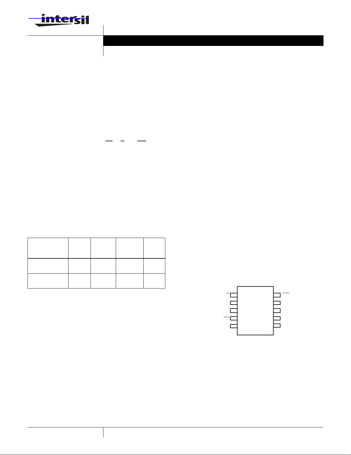
Pinout
ISL95710
(10 LD MSOP)
TOP VIEW
U/D
GND
CS
NC
1
V-
2
3
4
5
INC
10
VCC
9
R
8
L
R
W
7
R
6
H
FN8240.2
1
CAUTION: These devices are sensitive to electrostatic discharge; follow proper IC Handling Procedures.
1-888-INTERSIL or 1-888-468-3774
XDCP is a trademark of Intersil, Inc. Copyright Intersil Americas Inc. 2005. All Rights Reserved
| Intersil (and design) is a registered trademark of Intersil Americas Inc.
All other trademarks mentioned are the property of their respective owners.

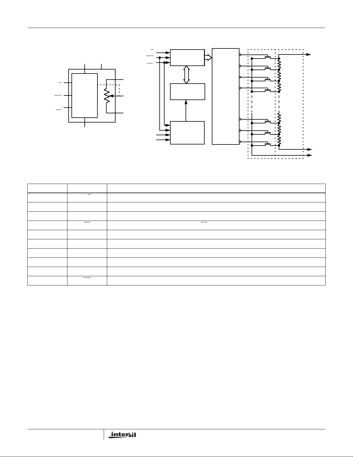
Block Diagram
ISL95710
V- (ANALOG VOLTAGE)
UP/DOWN
(U/D
INCREMENT
(INC
DEVICE SELECT
(CS
)
CONTROL
)
MEMORY
)
GND (GROUND)
GENERAL
AND
U/D
V
CC
R
H
R
W
R
L
INC
CS
VGND
7-BIT
UP/DOWN
COUNTER
7-BIT
NONVOLATILE
MEMORY
STORE AND
RECALL
CONTROL
CIRCUITRY
DECODER
Pin Descriptions
PIN NUMBER SYMBOL DESCRIPTION
1U/DControls the direction of wiper movement and whether the counter is incremented or decremented.
2 V- Negative bias voltage for the potentiometer wiper control.
3 GND Ground
4CS
5 NC No Connect. Pin is to be left unconnected.
6R
7R
8R
H
W
L
9 VCC Positive logic supply voltage.
10 INC
Chip select. The device is selected when the CS input is LOW. Also used to initiate a nonvolatile store.
A fixed terminal for one end of the potentiometer resistor.
The wiper terminal which is equivalent to the movable terminal of a potentiometer.
A fixed terminal for one end of the potentiometer resistor.
Increment input; negative edge triggered.
ONE
OF
128
127
126
125
124
2
1
0
DETAILED
TRANSFER
GATES
RESISTOR
ARRAY
R
H
R
L
R
W
2
FN8240.2
August 17, 2005

ISL95710
Absolute Maximum Ratings Thermal Information
Temperature under bias . . . . . . . . . . . . . . . . . . . . . . -65°C to +135°C
Storage temperature . . . . . . . . . . . . . . . . . . . . . . . .-65°C to +150°C
Voltage on CS
, INC, U/D and VCC
with respect to GND . . . . . . . . . . . . . . . . . . . . . . . . . . . -1V to +6V
Voltage on V- (referenced to GND) . . . . . . . . . . . . . . . . . . . . . . . -6V
∆V = |V
(RH)-V(RL)
| . . . . . . . . . . . . . . . . . . . . . . . . . . . . . . . . . .12V
Lead temperature (soldering 10 seconds) . . . . . . . . . . . . . . . .300°C
I
(10 seconds) . . . . . . . . . . . . . . . . . . . . . . . . . . . . . . . . . . . . ±6mA
W
ESD (Mil-Std 883, Method 3015) . . . . . . . . . . . . . . . . . . . . . . . . >2kV
ESD Machine Model . . . . . . . . . . . . . . . . . . . . . . . . . . . . . . . .>150V
CAUTION: Stresses above those listed under “Absolute Maximum Ratings” may cause permanent damage to the device. This is a stress rating only; functional
operation of the device (at these or any other conditions above those listed in the operational sections of this specification) is not implied. Exposure to absolute
maximum rating conditions for extended periods may affect device reliability.
NOTE:
is measured with the component mounted on a high effective thermal conductivity test board in free air. See Tech Brief TB379 for details.
3. θ
JA
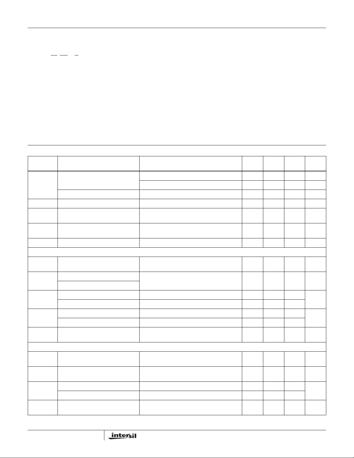
Analog Specifications Over recommended operating conditions unless otherwise stated.
SYMBOL PARAMETER TEST CONDITIONS MIN
R
TOTAL
RH to RL resistance W option 10 kΩ
U option 50 kΩ
R
to RL resistance tolerance -20 +20 %
H
V
RH,VRLRH,RL
R
W
C
H/CL/CW
I
LkgDCP
VOLTAGE DIVIDER MODE (V- @ R
INL
terminal voltage V- V
Wiper resistance V- = -5.5V; VCC = +5.5V, wiper current =
(V
-V-)/R
CC
TOTAL
Potentiometer Capacitance (Note 13) 10/10/
Leakage on DCP pins Voltage at pins; V- to V
; VCC @ RH; Voltage at RW = V
L
Integral non-linearity -1 1 LSB
(Note 6)
DNL
Differential non-linearity W, U options -0.5 0.5 LSB
(Note 5)
Thermal Resistance (Typical, Note 3) θ
MSOP Package . . . . . . . . . . . . . . . . . . . . . . . . . . . . 170
Recommended Operating Conditions
Temperature Range (Industrial) . . . . . . . . . . . . . . . . . -40°C to +85°C
V
. . . . . . . . . . . . . . . . . . . . . . . . . . . . . . . . . . . . . . . . 2.7V to 5.5V
CC
V- . . . . . . . . . . . . . . . . . . . . . . . . . . . . . . . . . . . . . . . . . -2.7V to -5.5V
TYP
(Note 1) MAX UNIT
70 200 Ω
25
-1 0.1 1 µA
RW
CC
unloaded)
CC
(°C/W)
JA
V
pF
(Note 2)
(Note 2)
ZSerror
Zero-scale error W option 0 1 4 LSB
(Note 3)
FSerror
Full-scale error W option -4 -1 0 LSB
(Note 4)
TC
(Notes 7,13)
Ratiometric Temperature Coefficient DCP Register set between 16 and 120d,
V
RESISTOR MODE (Measurements between R
RINL
Integral non-linearity DCP register set between 20 hex and 5F hex.
(Note 11)
RDNL
Differential non-linearity W, U options -0.5 0.5 MI
(Note 10)
Roffset
Offset DCP Register set to 00 hex, W option 0 2 5 MI
(Note 9)
TC
Resistance Temperature Coefficient DCP register set between 16 and 127d,
R
(Note 12,13)
3
U option 0 0.5 2
U option -2 -0.5 0
±4 ppm/°C
T = -40°C to +85°C
and RL with RH not connected, or between RW and RH with RL not connected)
W
-1 1 MI
Monotonic over all tap positions
DCP Register set to 00 hex, U option 0 0.5 2
±50 ppm/°C
T = -40°C to +85°C
(Note 2)
(Note 2)
(Note 8)
(Note 8)
(Note 8)
FN8240.2
August 17, 2005
 Loading...