

Page 1
®
Synchronous Buck Controller and One LDO
ISL9440CEVAL1Z: Triple PWM Step-Down
Application Note June 30, 2009
ISL9440CEVAL1Z Evaluation Board
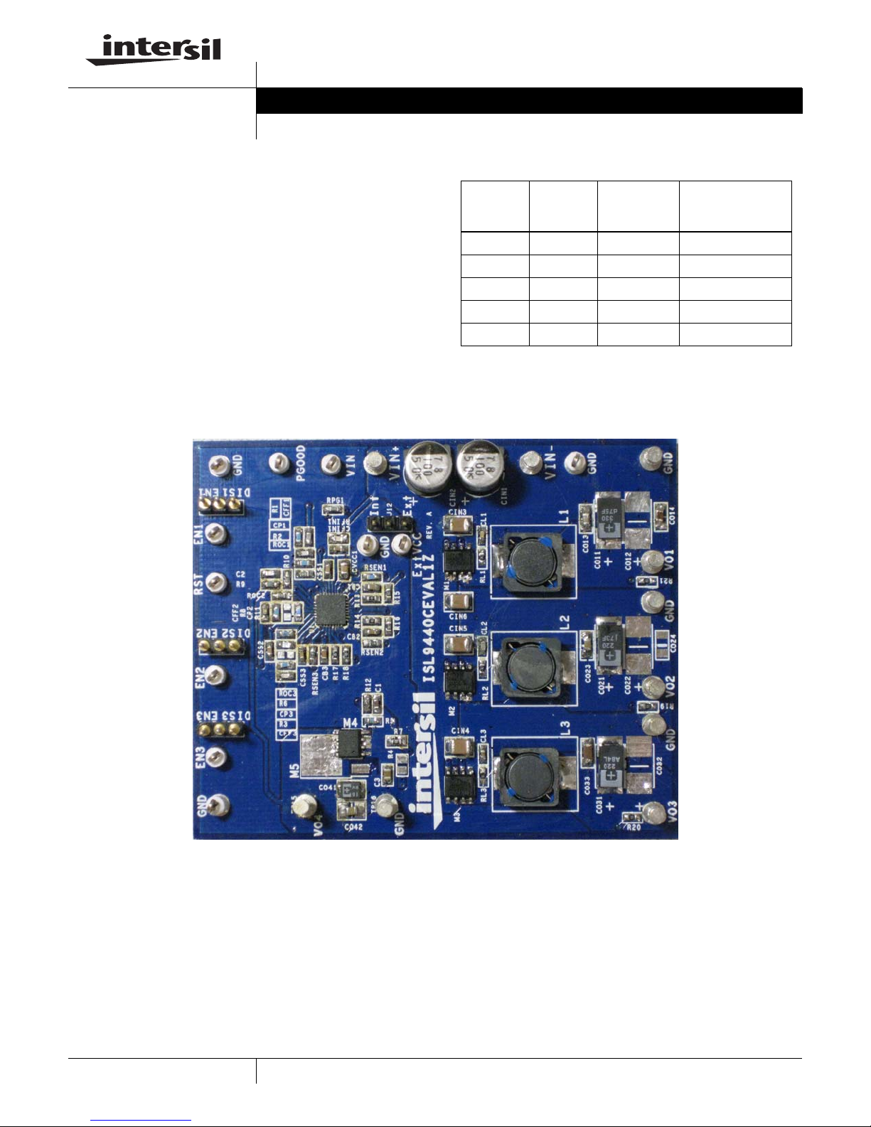
The ISL9440CEVAL1Z evaluation board features the
ISL9440C. The ISL9440C is quad-output controller that
integrates three PWM synchronous buck controllers and one
low-dropout linear regulator controller. The ISL9440C offers
programmable soft-start, independent enable functions and
integrates OV/OC/OT protection. The current mode control
architecture and internal compensation network keep
peripheral component counts minimized. 600kHz switching
frequency can minimize inductor size while the strong gate
driver is able to deliver 12A to each PWM channel.
Table 1 shows the difference in terms of ISL944xx family
features.
AN1482.0
TABLE 1. FEATURES OF ISL944xx FAMILY
SWITCHING
PART
NUMBER
ISL9440 YES 300 1.7
ISL9440A YES 600 1.7
ISL9441 NO 300 1.7
ISL9440B YES 300 PROGRAMMABLE
ISL9440C YES 600 PROGRAMMABLE
EARL Y
WARNING
FREQUENCY
(kHz)
The ISL9440CEVAL1Z is easy to set up to evaluate the
performance of the ISL9440C. Please refer to the “Electrical
Specifications” for typical performance summary.
SOFT-STARTING
TIME
(ms)
1
FIGURE 1. ISL9440CEVAL1Z EVALUATION BOARD
CAUTION: These devices are sensitive to electrostatic discharge; follow proper IC Handling Procedures.
1-888-INTERSIL or 1-888-468-3774
| Intersil (and design) is a registered trademark of Intersil Americas Inc.
All other trademarks mentioned are the property of their respective owners.
Copyright Intersil Americas Inc. 2009. All Rights Reserved
Page 2
Application Note 1482
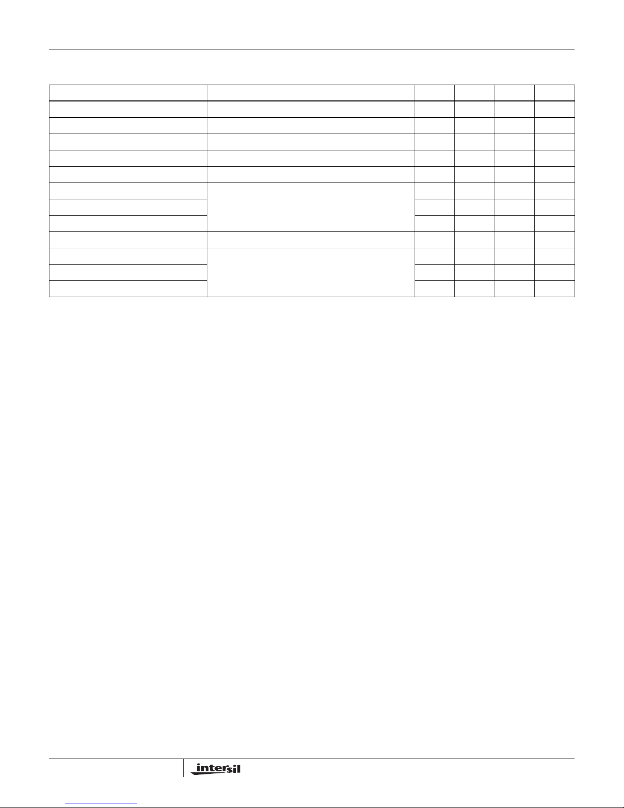
Electrical Specifications Recommended operation conditions unless otherwise noted. Refer to schematic and typical
performance curves.
PARAMETER TEST CONDITIONS MIN TYP MAX UNITS
V
IN
V
1 0.97 1.00 1.03 V
OUT
2 3.25 3.32 3.4 V
V
OUT
V
3 4.85 5.0 5.15 V
OUT
V
4 2.43 2.50 2.57 V
OUT
PWM1 Rated Current VIN =12V , TA = +25°C, No forced airflow, All three PWM
PWM2 Rated Current 67A
PWM3 Rated Current 45A
LDO Rated Current R7 = 0Ω, R4 is not populated 0.8 1.0 A
V
1 Peak-to-Peak Ripple V
OUT
V
2 Peak-to-Peak Ripple 59.6 mV
OUT
V
3 Peak-to-Peak Ripple 66.5 mV
OUT
All outputs are in regulation 6.0 12 16 V
67A
outputs are fully loaded
= 12V, All three PWM outputs are fully loaded,
IN
Oscilloscope is with full bandwidth
19.8 mV
P-P
P-P
P-P
What’s Inside
The Evaluation Board Kit contains the following materials:
• The ISL9440CEVAL1Z
• The ISL9440B, ISL9440C datasheet
• This EVAL KIT document
Recommended Equipment
The following materials are recommended to perform
testing:
• 0V to 20V Power Supply with at least 10A Source Current
Capability
• Three Electronic Loads Capable of Sinking Current up to 7A
• Digital Multimeters (DMMs)
• 100MHz Quad-Trace Oscilloscope
• Signal Generator (for load transient tests)
Quick Test Guide
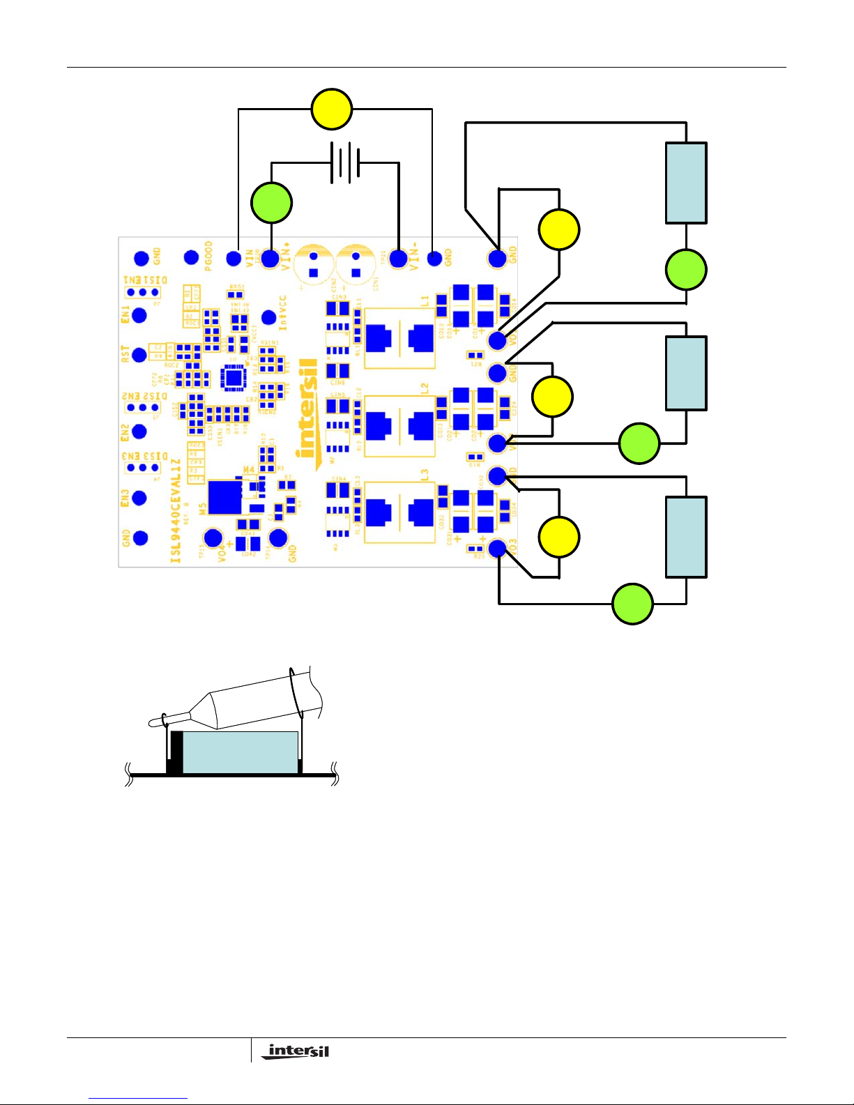
1. Ensure that the circuit is correctly connected to the supply
and electronic loads prior to applying any power. Please
refer to Figure 2 for proper set-up.
2. Connect Jumpers J3, J4 and J5 in the ENx positions.
3. Turn on the power supply
4. Adjust input voltage VIN within the sp ecified range and
observe output voltage. The output voltage variation
should be within 3%.
5. Adjust load current within the specified range and
observe output voltage. The output voltage variation
should be within 3%.
6. Use oscilloscope to observe output voltage ripple and
Phase node ringing. For accurate measurement, refer to
Figure 3 for proper test set-up.
2
AN1482.0
June 30, 2009
Page 3
Application Note 1482
V
+
_
A
+ VIN -
V
V
V
Vo2
Vo3
Vo1
_
+
_
+
+ -
_
+
+ -
Io2
A
Io3
Io1
A
LOADLOADLOAD
_
+
FIGURE 2. PROPER TEST SET-UP
OUTPUT CAP
OUTPUT CAP
OUTPUT CAP
OR MOSFET
OR MOSFET
OR MOSFET
FIGURE 3. PROPER PROBE SET-UP TO MEASURE OUTPUT
RIPPLE AND PHASE NODE RINGING
Load Transient Circuit Set-up
1. Select a SOIC8 N-Channel MOSFET with VDSS
breakdown > 20V.
2. Install the load transient circuit as indicated on the
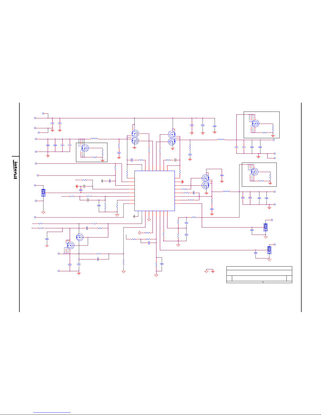
schematic. Refer to Figure 4 for detail.
A
3. R27, R22 and R25 are 10kΩ resistors for discharging the
MOSFET gates.
4. R26, R23 and R24 are current sensing resistors to
monitor the load step. For accurate measurement, please
use 5% tolerance sensing resistor or better. To alleviate
thermal stress, use 0.1Ω or smaller resistance. The
resistance of the sensing resistors sets the current scale
on the oscilloscope.
5. Apply pulse square waveform across R27, R22 or R25.
The duty cycle of the pulse waveform should be small
(<5%) to limit thermal stress on current sensing resistor
and the MOSFETs (M8, M6 or M7)
6. The amplitude of the clock sets the current step
amplitude. Adjust the clock amplitude and slew rate to set
the current step and slew rate.
7. Monitor overshoot and undershoot at corresponding
output.
3
AN1482.0
June 30, 2009
Page 4
Application Note 1482
.
OPT. LOAD TRAN.
OPT
M8
R26 OPT
FIGURE 4. LOAD TRANSIENT CIRCUIT FOR PWM1
Typical Evaluation Board Performance Curves V
90
VIN = 9VDC
85
80
75
70
65
60
EFFICIENCY (%)
55
50
45
40
08
VIN = 16VDC
1234567
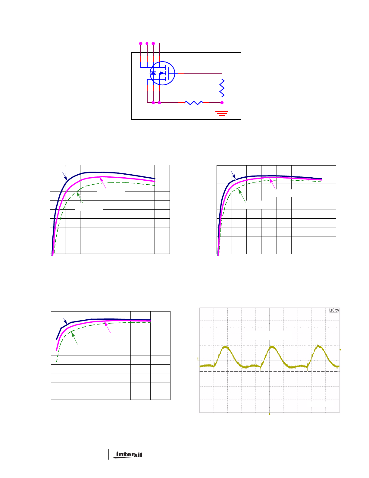
FIGURE 5. PWM1 EFFICIENCY vs LOAD (V
VIN = 12VDC
LOAD CURRENT (A)
= 1.0V) FIGURE 6. PWM2 EFFICIENCY vs LOAD (VO = 3.3V)
O
R27
OPT
= 12V, Unless Otherwise Noted.
IN
100
VIN = 9VDC
95
90
85
80
75
70
EFFICIENCY (%)
65
60
55
50
081234567
VIN = 16VDC
VIN = 12VDC
LOAD CURRENT (A)
100
VIN = 9VDC
95
90
VIN = 12VDC
LOAD CURRENT (A)
EFFICIENCY (%)
85
80
75
70
65
60
55
50
0246531
VIN = 16VDC
FIGURE 7. PWM3 EFFICIENCY vs LOAD (V
4
V
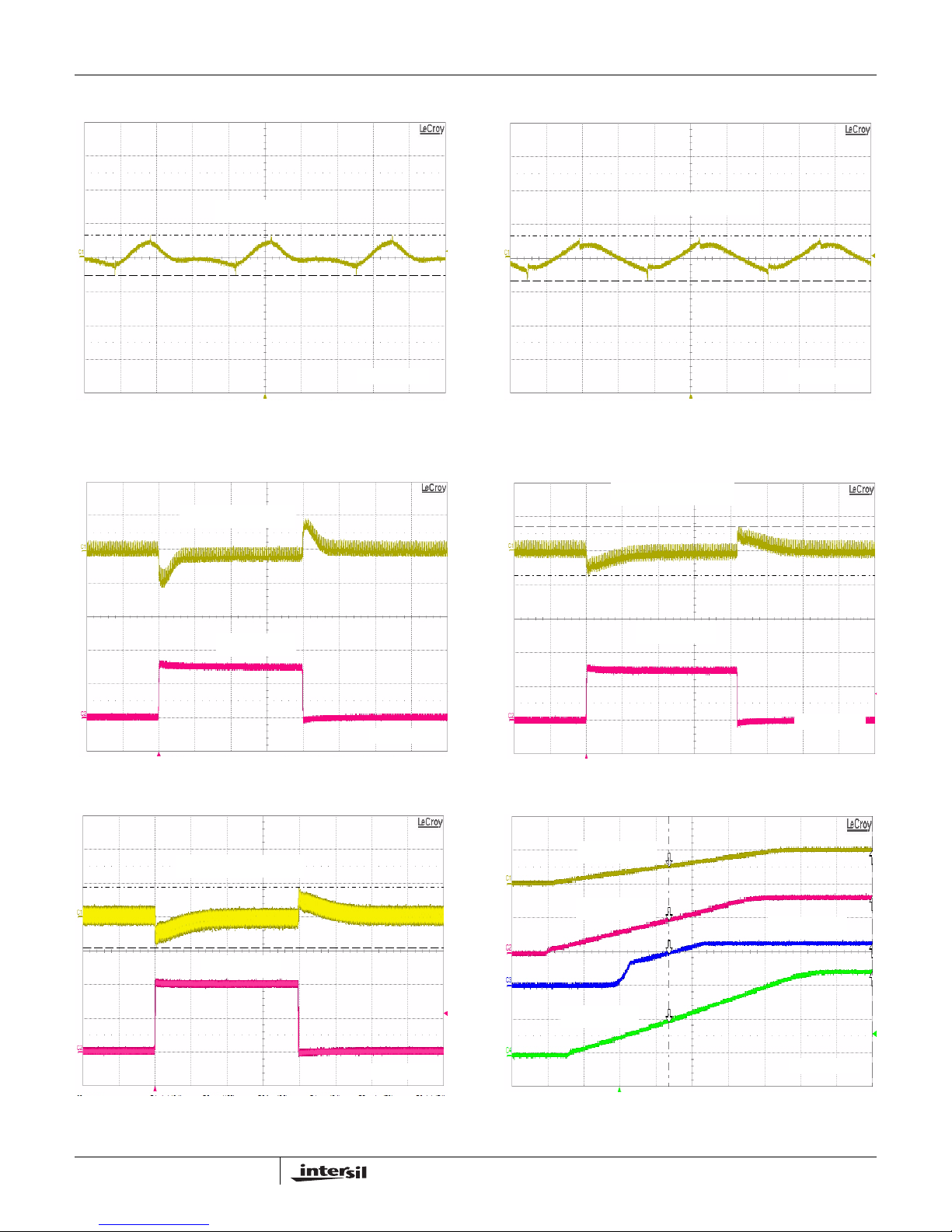
(AC), 10mV/DIV
OUT1
500n
s
= 5.0V) FIGURE 8. PWM1 OUTPUT RIPPLE UNDER MAX LOAD
O
(V
= 12V, IO1 = IO2 = 6A, IO3 = 4A, FULL
IN
BANDWIDTH)
June 30, 2009
/DIV
AN1482.0
Page 5
Application Note 1482
Typical Evaluation Board Performance Curves V
V
(AC), 50mV/DIV
OUT2
500ns/DIV
FIGURE 9. PWM2 OUTPUT RIPPLE UNDER MAX LOAD
(V
= 12V, IO1 = IO2 = 6A, IO3 = 4A, FULL
IN
BANDWIDTH)
V
(AC), 50mV/DIV
OUT1
= 12V, Unless Otherwise Noted. (Continued)
IN
V
(AC), 50mV/DIV
OUT3
500ns/DIV
FIGURE 10. PWM3 OUTPUT RIPPLE UNDER MAX LOAD
(V
= 12V, IO1 = IO2 = 6A, IO3 = 4A, FULL
IN
BANDWIDTH)
V
(AC, 100mV/DIV)
OUT2
I
, 2A/DIV
STEP
FIGURE 11. PWM1 LOAD TRANSIENT RESPONSE
(LOAD STEP FROM 1.5A TO 4.5A)
V
(AC), 100mV/DIV
OUT3
I
, 1A/DIV
STEP
50µs/DIV
50µs/DIV
I
, 2A/DIV
STEP
50µs/DIV
FIGURE 12. PWM2 LOAD TRANSIENT RESPONSE
(LOAD STEP FROM 1.5A TO 4.5A)
V
, 1V/DIV
OUT1
V
, 2V/DIV
OUT2
V
OUT4
V
, 2V/DIV
OUT3
1ms/DIV
, 2V/DIV
FIGURE 13. PWM3 LOAD TRANSIENT RESPONSE
(LOAD STEP FROM 1A TO 3A)
5
FIGURE 14. SOFT START WAVEFORMS
AN1482.0
June 30, 2009
Page 6
6
AN1482.0
June 30, 2009
Schematic
Titl e
Size Document Number Rev
Date: Sheet
of
<Doc> B
ISL9440CEVAL1Z EVALU ATION BOAR D
11Monday, May 11, 2009
UG2
VIN
Cp3
DNP
VO2
LG2
R23DNP
C2 22p
R21 0
PH1
CB20.1u
16V
Cf f 1 2.2n
CIN5
10u
25V
FB2
RL3
1.2
PH2
CL3
820p
VO1
R5 51
Ena ble d
M6
DNP
TP11
Int. VCC
1
TP3
PGOOD
1
Q1
Q2
M1
IRF7907
Q1
Q2
M3
IRF7907
R9 21. 5K 1%
Cp2
DNP
C1 0.22u
R13 0
CO22
DNP
6.3V
Enabled
Cp1
3.3n
CO24
10u
6.3V
TP15
VO4
1
CO23
DNP
10V
CO34
DNP
6.3V
LDOFB
Enabled
M5
DNP
R2
102K
1%
CFIN1 0.47u
35V
CIN4
10u
25V
TP4
RST
1
5V @ 4A
CIN1
100u
25V
Disabled
TP16
GND
1
FB3
J4
EN3
1
1
2
2
3
3
TP7
VO2
1
TP8
GND
1
VIN
R4 DNP
R25
DNP
UG1
Disabled
VO3
CIN6
10u
25V
SVIN
J5
EN2
1
1
2
2
3
3
Disabled
TP10
GND
1
TP9
VO3
1
LG3
R10
10K
1%
PH3
VO3
CO11
330u
2.0V
Sanyo, 2R5TPE330M7
CO13
10u
6.3V
CO14
10u
6.3V
LG1
ROC2 200K
CO12
DNP
6.3V
VO2
Cff 2 100p
U1
ISL9440C
ISEN1
1
PGOOD
2
VCC_5V
3
VIN
4
EN/SS1
5
FB1
6
OCSET1
7
RST_N
8
G49LDOFB10SGND11OCSET212FB213EN/SS214OCSET315FB3
16
EN/SS3
17
ISEN3
18
PHASE3
19
BOOT3
20
UGATE3
21
LGATE3
22
PGND
23
ISEN2
24
PHASE2
25
BOOT2
26
UGATE2
27
LGATE228LGATE1
29
UGATE1
30
BOOT1
31
PHASE1
32
33
PAD
TP19
GND
1
Css1
10n
TP1
VIN
1
RL1
1.2
CL1
820p
TP2
VIN-
1
1V @ 6A
LDOFB
VO1
CIN3
10u
25V
OPT. Load Tran.
OPT. Load Tran.
OPT. Load Tran.
Cff3
100p
3.3V @ 5.0A+1.0A
TP12
EN1
1
R140
RL2
1.2
CL2
820p
TP5
VO1
1
TP6
1
VIN+
CIN2
100u
25V
CVCC1
4.7u
16V
TP17
GND
1
R19 0
VCC5V
Css3
10n
R3
105K
1%
R8 107K 1%C3
1u
EN3
ROC1
100K
UG3
Css2
10n
R26DNP
CO41
10u
M8
DNP
CB10.1u
16V
R27
DNP
ROC3
200K
TP13
EN3
1
TP20
VIN
1
R24DNP
M7
DNP
VIN
TP21
GND
1
VIN
EN1
R170
R1 25.5K 1%
J3
EN1
1
1
2
2
3
3
CO32
DNP
6.3V
R18 0
CO33
10u
6.3V
2.5V @ 1.0A
VO2
CO31
220u
6.3V
Sanyo, 6TPE220MI
TP14
EN2
1
VIN-
RPG1
100K
L1 1.0u
TOKO, #919AS-1R0N
R11
34K
1%
M4
Si4423DY
CO42
100u
4.0V
4TPE100MZB
R22
DNP
CB3
0.1u
16V
PGOOD
R7 0
RFIN1 10
R15
0
Rsen1
1.82K
R20 0
CO21
220u
6.3V
Sanyo, 6TPE220MI
R16
0
Rsen3 3.32K
L2 1.8u
TOKO, #919AS-1R8N
R12 0
L3 2.8u
TOKO, #919AS-2R8M
Q1
Q2
M2
IRF7907
Rsen2
3.32K
R6
20K
1%
Application Note 1482
Page 7
Application Note 1482
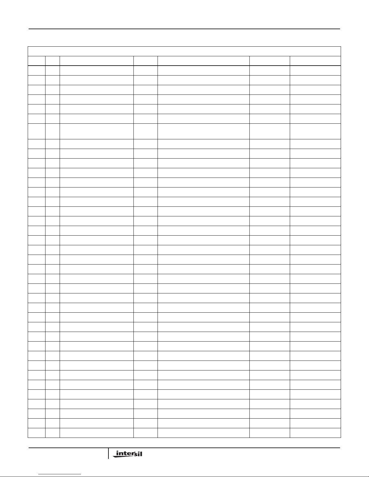
TABLE 2. BILL OF MATERIALS
ESSENTIAL COMPONENTS
ITEM QTY PART REFERENCE VALUE DESCRIPTION PART # MANUFACTURER
1 3 CB1, CB2, CB3 0.1µF CAP Ceramic X5R, 16V, SMD, 0603, Generic
2 1 CFIN1 0.47µF CAP Ceramic X5R, 25V, SMD, 0603, Generic
3 2 CIN1, CIN2 100µF Alum. Elec. CAP 25V Panasonic
4 4 CIN3, CIN4, CIN5, CIN6 10µF CAP Ceramic X5R, 25V, SMD, 1206, Generic
5 3 CL1, CL2, CL3 820pF CAP Ceramic X5R, 16V, SMD, 0603, Generic
6 1 CO11 330µF POSCAP, 2.0V, SMD, D2E 2R5TPE330M7 Sanyo
7 5 CO13, CO14, CO24, CO33,
CO41
8 2 CO21, CO31 220µF POSCAP, 6.3V, SMD, D2E 6TPE220MI Sanyo
9 1 CO42 100µF POSCAP, 4.0V, SMD, B 4TPE100MZB Sanyo
10 1 CVCC1 4.7µF CAP Ceramic X5R, 16V, SMD, 0805, Generic
11 1 Cff1 2.2nF CAP Ceramic, SMD, 0603, Generic
12 2 Cff2, Cff3 100pF CAP Ceramic, SMD, 0603, Generic
13 1 Cp1 3.3nF CAP Ceramic, SMD, 0603, Generic
14 3 Css1, Css2, Css3 10nF CAP Ceramic, SMD, 0603, Generic
15 1 C1 0.22µF CAP Ceramic X5R, 16V, SMD, 0603, Generic
16 1 C2 22pF CAP Ceramic, SMD, 0603, Generic
17 1 C3 1µF CAP Ceramic, 6.3V,SMD, 0603, Generic
18 1 L1 1.0µH SHIELDED INDUCTOR #919AS-1R0N TOKO
19 1 L2 1.8µH SHIELDED INDUCTOR #919AS-1R8N TOKO
20 1 L3 2.8µH SHIELDED INDUCTOR #919AS-2R8M TOKO
21 3 M1, M2, M3 Dual N MOSFET, 30V , SOIC8 IRF7907 International Rectifier
22 1 M4 P MOSFET, SOIC8 Si4423DY Vishay
23 1 R
FIN1
24 3 RL1, RL2, RL3 1.2Ω RESISTOR, SMD, 0603, 10% Generic
25 2 RPG1, ROC1 100kΩ RESISTOR, SMD, 0603,1% Generic
26 2 ROC2, ROC3 200kΩ RESISTOR, SMD, 0603,1% Generic
27 1 R
28 2 R
SEN1
SEN2
, R
SEN3
29 1 R1 25.5kΩ RESISTOR, SMD, 0603,1% Generic
30 1 R2 102kΩ RESISTOR, SMD, 0603,1% Generic
31 1 R3 105kΩ RESISTOR, SMD, 0603,1% Generic
32 1 R5 51Ω RESISTOR, SMD, 0603,1% Generic
33 1 R6 20kΩ RESISTOR, SMD, 0603,1% Generic
34 1 R8 107kΩ RESISTOR, SMD, 0603,1% Generic
35 1 R9 21.5kΩ RESISTOR, SMD, 0603,1% Generic
36 1 R10 10kΩ RESISTOR, SMD, 0603,1% Generic
37 1 R11 34kΩ RESISTOR, SMD, 0603,1% Generic
38 1 U1 - QUAD OUTPUT CONTROLLER ISL9440C Intersil
10µF CAP Ceramic X5R, 6.3V, SMD, 0805 Generic
10Ω RESISTOR, SMD, 0805, 10% Generic
1.82kΩ RESISTOR, SMD, 0603,1% Generic
3.32kΩ RESISTOR, SMD, 0603,1% Generic
7
AN1482.0
June 30, 2009
Page 8
Application Note 1482
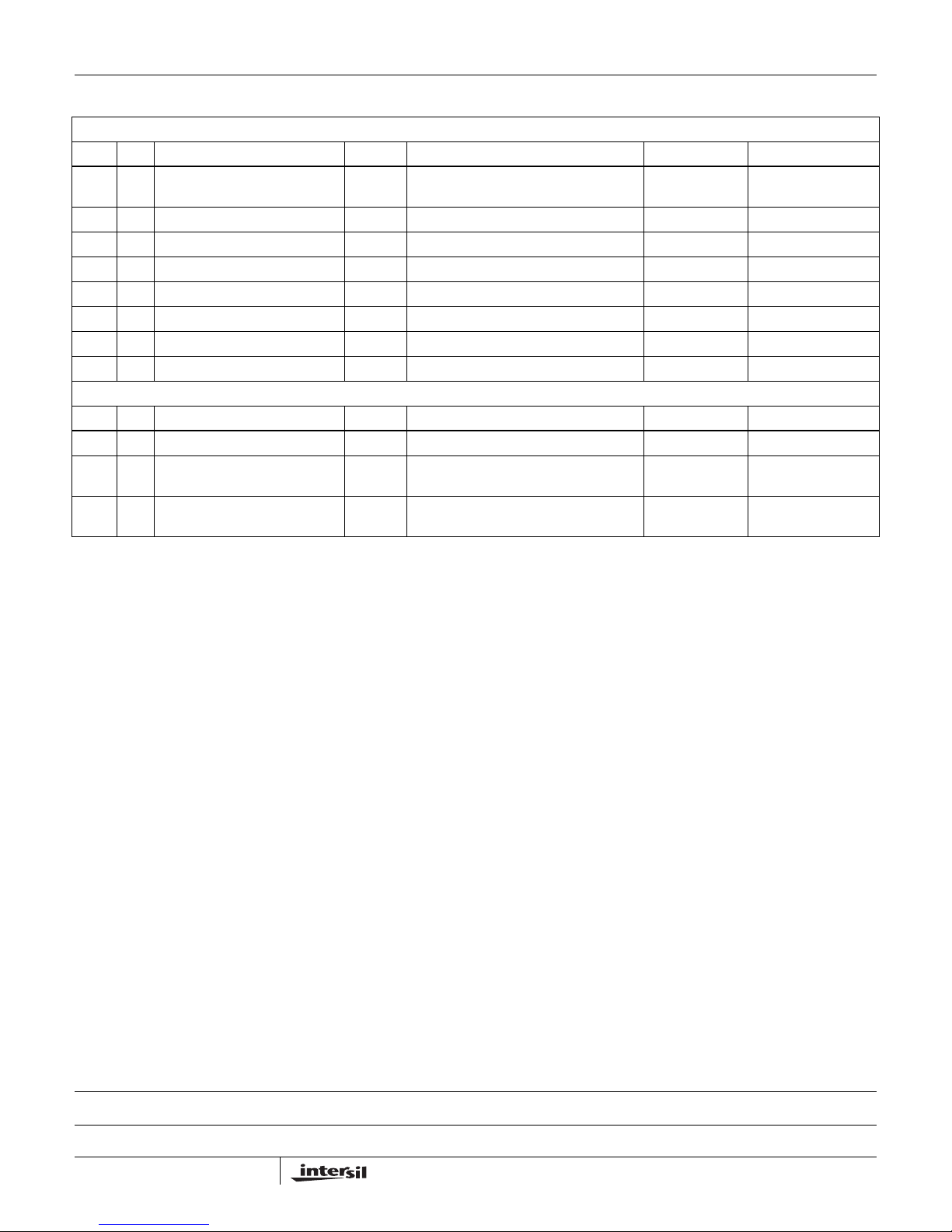
TABLE 2. BILL OF MATERIALS (Continued)
OPTIONAL COMPONENTS OR RESISTOR JUMPERS
ITEM QTY REFERENCE VALUE DESCRIPTION PART # MANUFACTURER
39 10 R7, R12, R13, R14, R15, R16,
R17, R18, R19, R20, R21
40 3 CO12, CO22, CO32 DNP
41 2 CO23, CO34 DNP
42 2 Cp2, Cp3 DNP
43 1 M5 DNP P MOSFET TO-252
44 3 M6, M7, M8 DNP N MOSFET
45 4 R4, R22, R25, R27 DNP RESISTOR, SMD, 0603
46 3 R23, R24, R26 DNP RESISTOR, SMD, 1206
ITEM QTY REFERENCE VALUE DESCRIPTION PART # MANUFACTURER
47 3 J3, J4, J5 - 3 Head Jumper 68000-236HLF Generic
48 11 TP1, TP2, TP3, TP4, TP6, TP17,
TP11, TP12, TP13, TP14, TP7
49 9 TP8, TP10, TP16, TP19, TP21,
TP9, TP5, TP15, TP20
0 RESISTOR Jumpers, SMD, 0603, 10% Generic
EVALUATION BOARD HARDWARES
- TEST POINT 5007 Keystone
GND TURRET 1514-2 Keystone
Intersil Corporation reserves the right to make changes in circuit design, software and/or specifications at any time without notice. Accordingly, the reader is cautioned to
verify that the Application Note or Technical Brief is current before proceeding.
For information regarding Intersil Corporation and its products, see www.intersil.com
8
AN1482.0
June 30, 2009
Page 9
9
AN1482.0
June 30, 2009
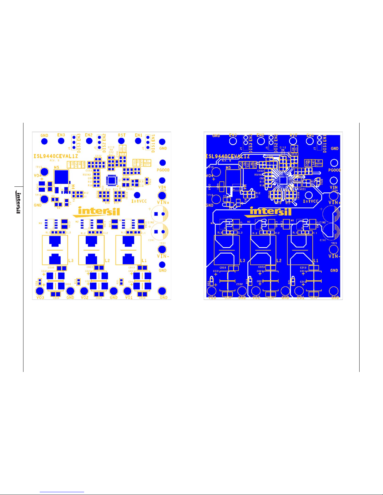
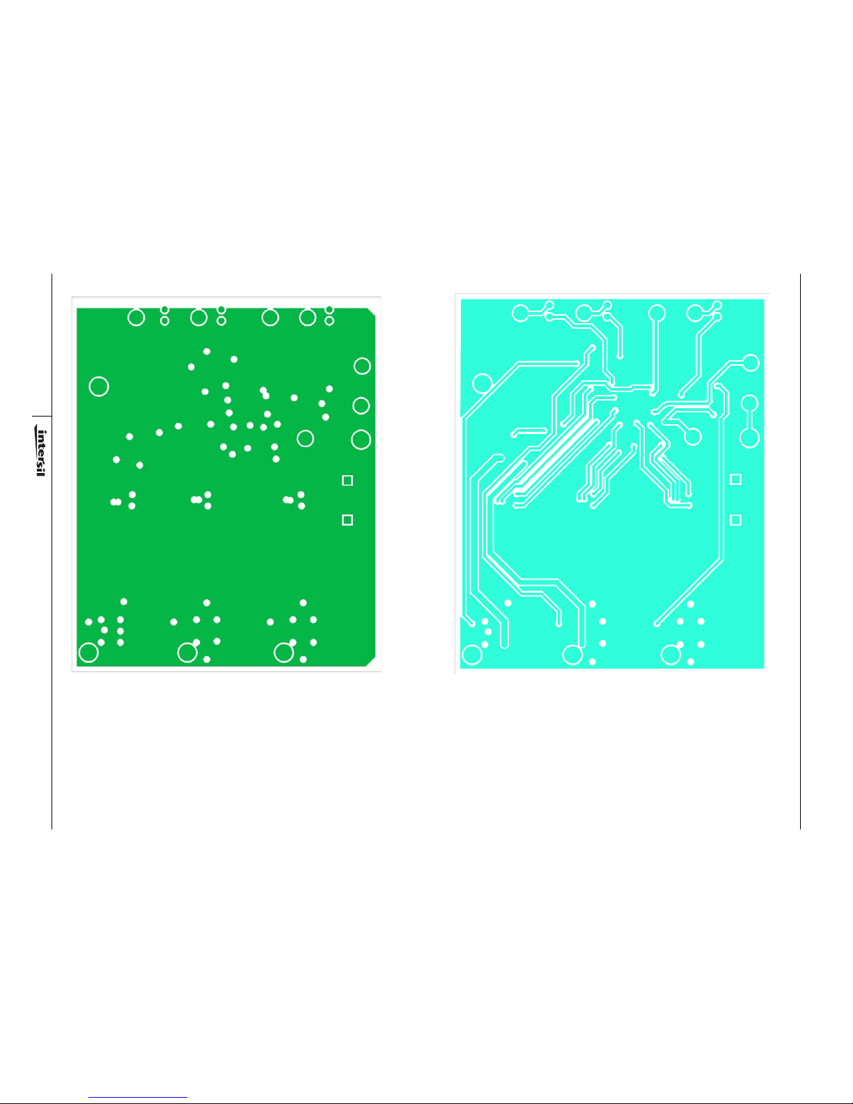
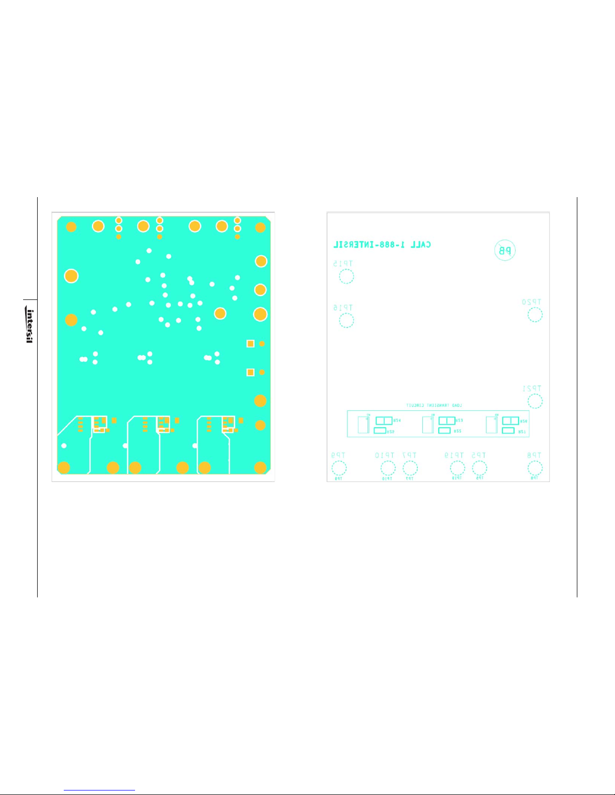
ISL9440CEVAL1Z PCB Layout
FIGURE 15. TOP COMPONENTS
FIGURE 16. TOP LAYER
Application Note 1482
Page 10
10
AN1482.0
June 30, 2009
FIGURE 17. SECOND LAYER (SOLID GROUND)
FIGURE 18. THIRD LAYER
ISL9440CEVAL1Z PCB Layout (Continued)
Application Note 1482
Page 11
11
AN1482.0
June 30, 2009
FIGURE 19. BOTTOM LAYER (MIRRORED)
FIGURE 20. BOTTOM COMPONENTS (MIRRORED)
ISL9440CEVAL1Z PCB Layout (Continued)
Application Note 1482
Page 12

Mouser Electronics
Authorized Distributor
Click to View Pricing, Inventory, Delivery & Lifecycle Information:
Intersil:
ISL9440CEVAL1Z
 Loading...