

Page 1
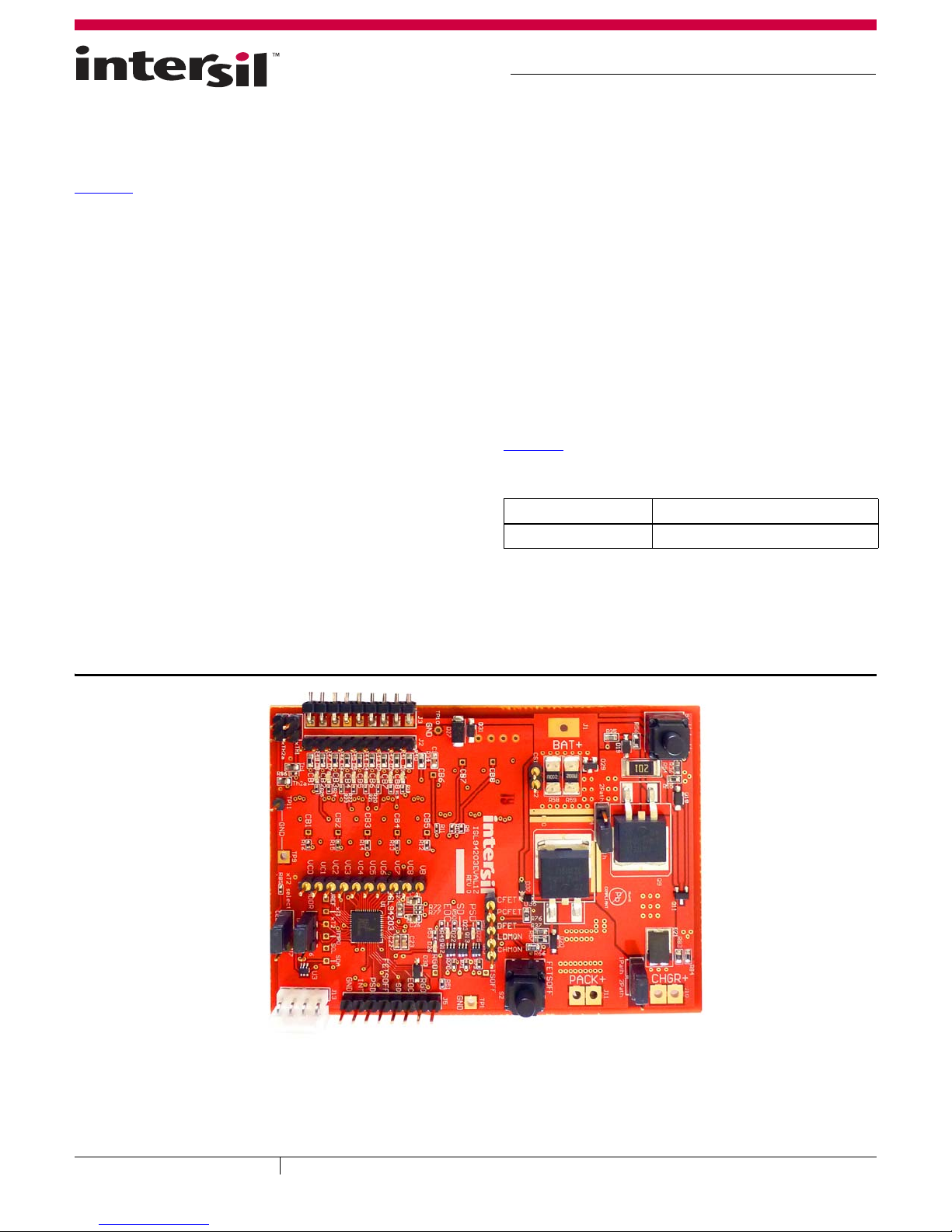
FIGURE 1. ISL94203EVKIT1Z EVALUATION BOARD
Application Note 1952
ISL94203EVKIT1Z Evaluation Kit User Guide
The ISL94203EVKIT1Z is a kit that facilitates testing of the
ISL94203 Li-ion battery pack monitor and control ICs. The
ISL94203 monitors cell voltage, current and temperature. It
converts the cell voltages, pack current and temperatures to
12-bit digital values, provides cell balance control and provides
complete stand-alone battery pack operation.
The ISL94203 default stand-alone operation can be overridden
by an external microcontroller. The PC graphical user interface
(GUI) supports the hooks needed to monitor stand-alone
operation and to demonstrate operation with an external
microcontroller.
Specifications
This board has been configured and optimized for the following
operating conditions:
• Configurable to 3 to 8 cells, default 3 cells
• Standard cell voltage range 2.699V to 4.250V
• OV/UV delay times 1 and 4 seconds respectively
• CB max delta voltage 0.501
• CB max/min voltage 4.032V and 3.100V
NOTE: Consult programming options for full listing of programmable
parameters and ranges.
Key Features
• Status LEDs monitor RGO, EOC, SD and PSD conditions
• Jumper configuration single or split path applications
• Wakeup push button for "Exit Sleep" control
• FETs off push button for quick all FETs off condition
• Cell balance LEDs for MCB process observation
• PCB layout accommodates "solder braid" addition for high
current evaluation
• Software enables real time observation and data collection
of 14 analog measurements and 27 digital status indicators
References
ISL94203 Datasheet
Ordering Information
PART NUMBER DESCRIPTION
ISL94203EVKIT1Z Evaluation kit for the ISL94203
July 30, 2015
AN1952.1
1
CAUTION: These devices are sensitive to electrostatic discharge; follow proper IC Handling Procedures.
1-888-INTERSIL or 1-888-468-3774
Intersil (and design) is a trademark owned by Intersil Corporation or one of its subsidiaries.
| Copyright Intersil Americas LLC 2014, 2015. All Rights Reserved
All other trademarks mentioned are the property of their respective owners.
Page 2

Application Note 1952
What is Inside
The Evaluation Kit contains:
• ISL94203 evaluation board
• MCB_PS_Z multicell power supply test board
• ISL94203INTFACEKIT1Z USB to I
PCB and I2C cable
• USB cable, connects PC to USB-I2C interface board
2
C interface kit, includes a
What is Needed
The following instruments will be needed to perform testing:
• 30V/1A adjustable power supply
• Wires to connect power supply to MCB_PS_Z board
• Precision multimeter (optional)
• Oscilloscope (optional)
• Cables and wires (optional)
Software Installation
Step 1: Connect the ISLUSBI2C USB to the PC. The board
should automatically enumerate in the device control
panel under Human Interface Devices. The vendor ID
will be 0x09AA and the product ID will be 0x2036.
Since it is a HID device, no special driver is needed.
Step 2: Copy the Intersil_ISL94203_Installer_Vxxx.exe
program to the PC (any desired location). Double-click
to run the installation file. Note you may need to use
the “Run as Administrator” open when performing the
installation.file.
Quick Hardware Setup Guide
Step 1: Check the jumpers and switches on the board. The
board should be configured as follows:
• ADDR jumper set to “0”.
• xT2 Select jumper on either “CELL” or “FET”.
• FET jumpers set for either one path or two path.
Start with one path.
• J4 jumper is set to “1 Path”.
J9 jumper is set to “1 Path”.
Step 2: Connect the power supply to the MCB_PS_Z board. The
positive terminal is J5/J11 and the negative terminal is
J8/J12. There should be a jumper on JP2/8CELL.
Step 3: Set the power supply voltage to 28V (3.5V per cell).
(Optional: check that the voltages at terminal J1 or J3
are 3.5V per cell).
Step 5: Connect the ISL94203 board directly to the MCB_PS_Z
board at connector J1. Make sure the board is
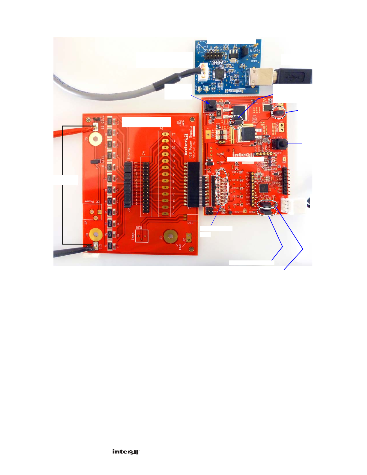
connected on the ground side of J1 (see Figure 2
Step 6: Turn on the power to the supply. If no LEDs light, press
the “WakeUp” button. Notice that there is one green
LED (RGO), indicating the LDO regulator on the
ISL94203 is operating.
The voltages at various points should be:
RGO = 2.5V ±3%
VREF = 1.80V ±0.5%
Step 7: Connect the USB port of the PC to the USB port of the
ISL94203INTFACEKIT1Z interface board.
Step 8: Connect the I
ISL94203INTFACEKIT1Z board to the
ISL94203EVKIT1Z board (J13).
Step 9: Open the ISL94203 GUI software. Use the software to
read the cell voltages.
Step 10: Compare the voltages at the board input (use a meter
to measure each input voltage, because the MCB_PS_Z
board may not accurately divide the voltages into equal
3.5V steps) with the readings provided by the GUI.
These voltages should closely match.
Step 11: See other operations described later in this document.
2
C cable from the
).
PCB Layout Guidelines
The AC performance of this circuit depends greatly on the care
taken in designing the PC board. The following are
recommendations to achieve optimum high performance from
your PC board.
• The use of low inductance components, such as chip resistors
and chip capacitors, is strongly recommended.
• Minimize signal trace lengths. This is especially true for the
VDD, charge pump decoupling, CS1, CS2, and VC0-VC8 inputs.
Trace inductance and capacitance can easily affect circuit
performance. Vias in the signal lines add inductance at high
frequency and should be avoided.
• Match channel-to-channel analog I/O trace lengths and layout
symmetry. This is especially true for the CS1 and CS2 lines,
since their inputs are normally very low voltage.
• Maximize use of AC decoupled PCB layers. All signal I/O lines
should be routed over continuous ground planes (i.e., no split
planes or PCB gaps under these lines). Avoid vias in the signal
I/O lines.
• When testing, use good quality connectors and cables,
matching cable types and keeping cable lengths to a
minimum.
Step 4: Turn off the power to the power supply.
Submit Document Feedback
2
AN1952.1
July 30, 2015
Page 3
Application Note 1952
FIGURE 2. ISL94203EVKIT1Z BOARD SETUP
ISL94203EVKIT1Z
MCB_PS_Z BOARD
SET I2C ADDR
SET xT2 THERMISTOR
TO FET OR TO CELL
CELL BALANCE
LEDs
ISL94203INTFACEKIT1Z
TO PC USB PORT
WAKE UP
CONTROL
TO USB-I2C
BOARD
I
2
C PORT
FETSOFF
MANUAL
CONTROL
ISL94203EVKIT1Z BOARD
I
2
C PORT TO
SETS CHMON
TO 1 PATH OR
2 PATH
6V TO 38V
SETS POWER PATH
(CHARGE/DISCHARGE)
1 PATH OR 2 PATH)
Submit Document Feedback
3
AN1952.1
July 30, 2015
Page 4
Application Note 1952
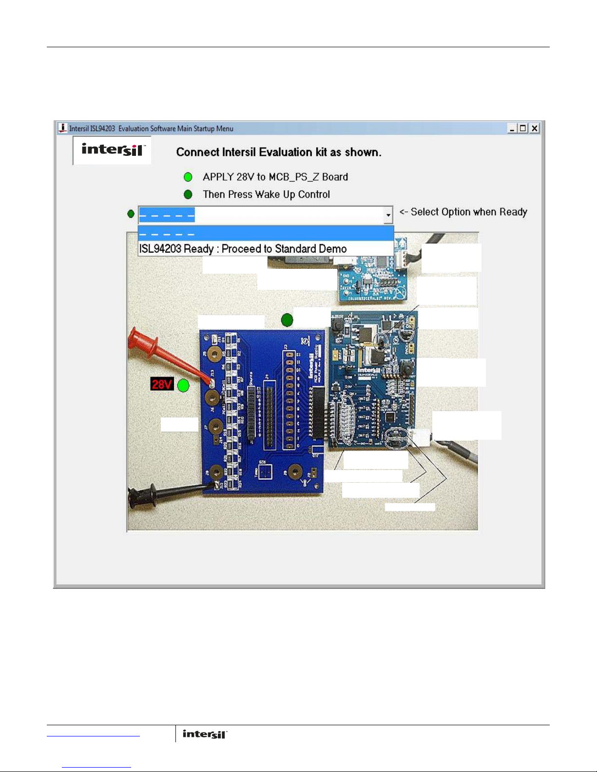
FIGURE 3. MAIN GUI START-UP WINDOW
ISL94203INTFACEKIT1Z
I2C PORT
TO EVAL BOARD
SETS 1
DISCHARGE PATH
SETS CHMON
TO 1 PATH
FETSOFF
MANUAL CONTROL
I2C PORT
TO USE
USB-I2C BOARD
ISL94203EVKIT1Z
MC3_PS_Z BOARD
WAKE UP
CONTROL
6V TO 38V
TO PC USB PORT
SET I2C ADDR
SET XT2 THERMISTOR
TO FET OR TO CELL
CELL BALANCE LEDs
Quick GUI Setup Guide
Step 1: Once the board is powered up and connected to the PC
through the USB cable, start the GUI program. Then
click on the dropdown box.
Submit Document Feedback
4
AN1952.1
July 30, 2015
Page 5
Application Note 1952
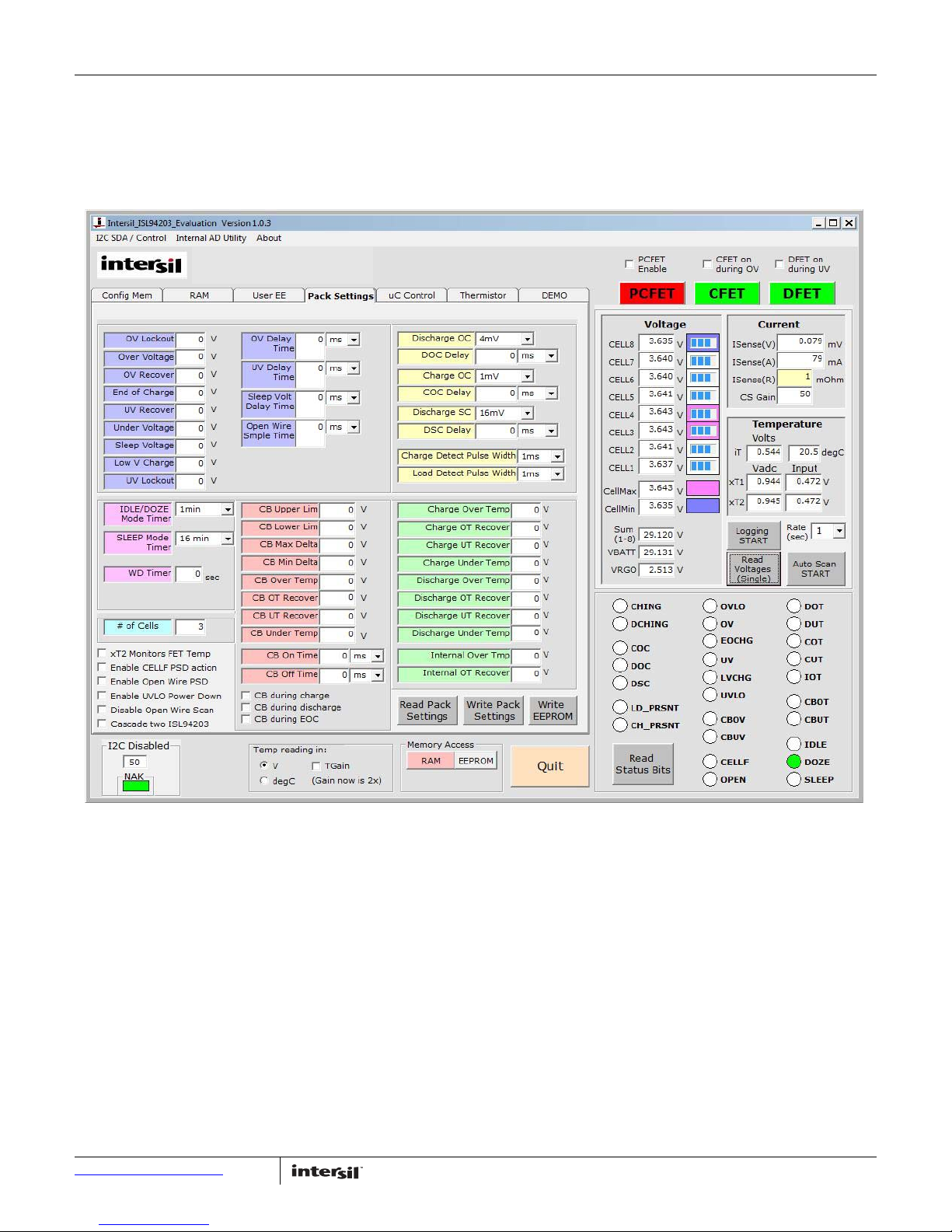
FIGURE 4. MAIN GUI WINDOW SHOWING PACK SETTINGS
ISL94203EVKIT1Z
Step 2: Click on “Read Voltages (Single).” This updates all the
cell voltages, temperature and current readings, and
updates the status indicators.
Step 3: Click on “Read Pack Settings.” This returns the
configuration parameters set in the device.
Step 4: Review the operation of the GUI features in the
following sections.
Submit Document Feedback
5
AN1952.1
July 30, 2015
Page 6
Application Note 1952
FIGURE 5.
FIGURE 6.
Using the GUI
Common Screen
The right side of the GUI shows the status of the ISL94203. At the
top are voltage, current and temperature readings. The bottom
are the status bits.
At the bottom of the screen are several controls for temperature
settings and memory access.
CELL VOLTAGE SCANS
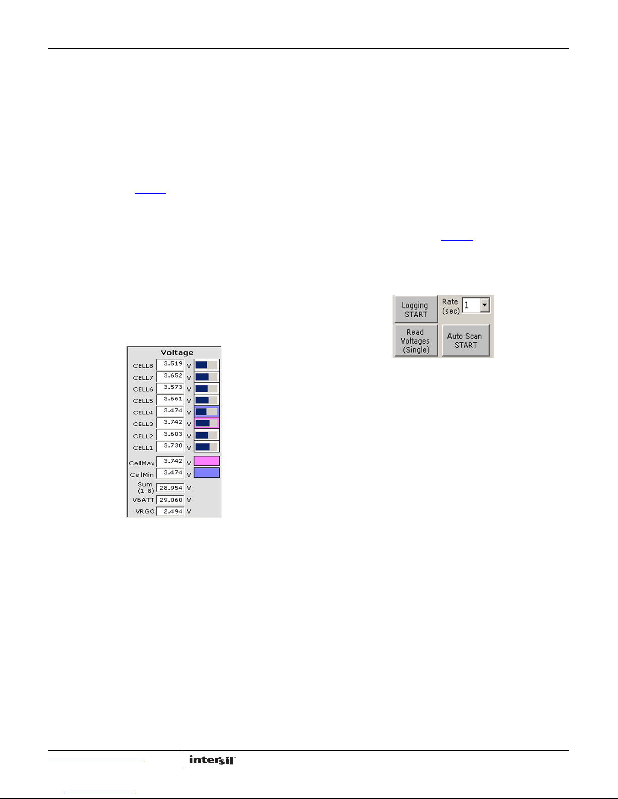
The voltage readouts (Figure 5) show the values for each cell,
plus CELLMAX and CELLMIN values. The CELLMAX and CELLMIN
values are returned from the ISL94203 registers. To properly
implement this operation, the GUI stops the internal voltage scan
of the ISL94203 (using the µCSCAN bit). It then reads the cell
voltages and CELLMAX and CELLMIN values and restarts the
automatic scan of the device. The values are read
asynchronously, so without stopping the scan there is not
sufficient time to read all the values prior to the next internal
scan. For this reason the CELLMIN and CELLMAX values are often
reported from a different scan than the rest of the cell voltages.
Also, during the scan, the cell balance operation is stopped. This
is so the cell balance currents do not cause false readings of the
cell voltages, due to external voltage drops.
indication from the device is shown by the UV and OV status
indicators (bottom right of the screen). These indicators come
directly from the device status bits.
Below the CellMIN and CellMAX readings are three boxes that
show additional voltage values. The top box contains the sum of
the individual cell readings. The middle box shows the voltage
reading of the total battery pack as derived from an internal
divide by 16 voltage divider and converted by the ADC.
Comparing these two values allows a gross determination if
there is a cell voltage failure.
The bottom box shows the voltage of the 2.5V regulator. The
regulator voltage is internally divided by 2, then converted by the
ADC and multiplied by 2 prior to display.
Pressing the “Read Voltages (Single)” button completes one read
of the values in the device, (see Figure 6
voltages and the status bits. Between presses of this button, the
device continues to scan the voltage, current and temperature
values at the rate of 32ms (or 256ms if in IDLE mode, or 512ms
if in DOZE mode).
). This includes all of the
To the right of the cell voltages, there is a graphic indication of
the capacity of the cell. This is based on the voltage of the cell. In
this graphic depiction, the scale shows no bar when the voltage is
less than or equal to the undervoltage threshold. It shows 100%,
or maximum, when the cell voltage is equal to or greater than the
overvoltage threshold. See the overvoltage and undervoltage
thresholds in the Pack settings tab on the left of the screen.
The GUI highlights the specific cells that equal the CELLMAX and
CELLMIN voltages. This helps to identify which cells are high or
low on quick inspection.
When any cell voltage is lower than the undervoltage level, or
higher than the overvoltage level, the background color of that
voltage readout changes to red. When the voltage rises above the
UV recovery voltage or drops below the OV recovery voltage the
background color returns to white. These color changes are GUI
representations of the cell voltage conditions, the actual
Pressing the “Auto Scan START” button starts a repetitive update
of the values. The rate of update is set by the “Rate (sec)”
dropdown box. As shown, the GUI updates the voltages and
status every 1 second. Autoscan is stopped by pressing the
autoscan “STOP” button. While the autoscan is operating, all
other memory accesses are prohibited. To read the pack settings
or change a register value, first stop the automatic scan.
To log the data, press “Logging START” prior to clicking on the
“Auto Scan START” button. The data will be stored as a text
document in a file location specified by the user. When all data
has been captured, stop the auto scan and stop logging.
Submit Document Feedback
6
AN1952.1
July 30, 2015
Page 7
Application Note 1952
FIGURE 7. TEMPERATURE READINGS
(EQ. 1)
TGAIN 0=
intTemp mV
1.8527
---------------------------------------
273.15– ICTemp C=
(EQ. 2)
TGAIN 1=
intTemp mV
0.92635
---------------------------------------
273.15– ICTemp C=
FIGURE 8. TEMPERATURE READINGS DISPLAYED IN °C
TEMPERATURE READINGS
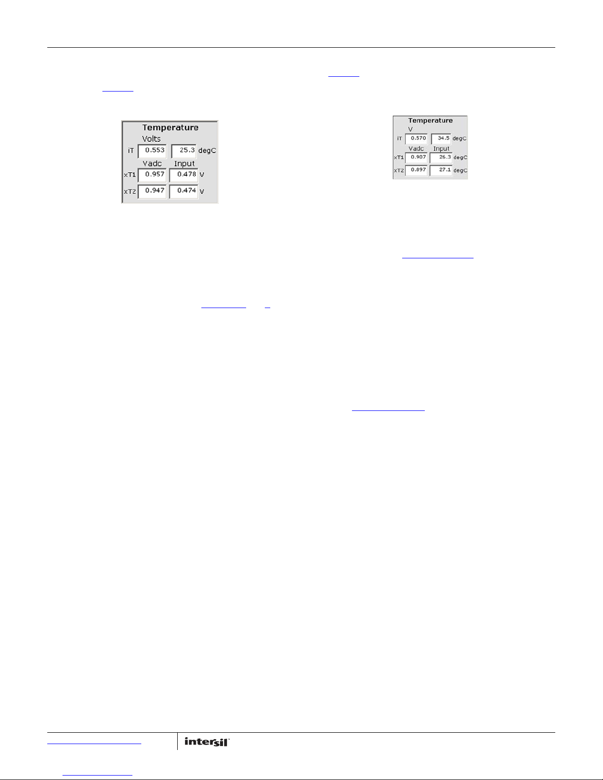
To the right of the pack voltage values are the temperature
readings, (see Figure 7). In the default state, these boxes report
the voltage on the temperature inputs. There are two boxes for
each temperature.
The internal temperature reading (at the top) has two boxes. The
left box shows the voltage reading from the internal temperature
sensor. This voltage is dependent on the setting of the
temperature gain bit (TGAIN). The temperature gain can be
changed using the GUI by clicking the “TGAIN” button in the
temperature box in the bottom left of the screen (below the tabs).
The box on the right shows the conversion of the internal
temperature to °C. This conversion uses Equations 1
For the external temperatures, the left box shows the digital
reading from the ADC. The right box shows the applied input
voltage. The value on the left is dependent on the setting of the
TGAIN bit. If TGAIN = 0, then the temperature input voltage is
multiplied by 2 prior to being read by the ADC. If TGAIN = 1, then
the temperature input voltage is multiplied by 1. The left box of
the external temperature readings simply translates the voltage
readout by the ADC. The right box calculates the input voltage,
based on the setting of the TGAIN bit.
and 2:
The temperature readings can also be displayed in °C,
(see Figure 8
). The conversion to °C depends on several items.
First is the gain setting, so the actual input voltage is known.
Second is the external resistor divider components. Third is the
conversion of the thermistor value to °C.
The gain setting is important only for determining the voltage
applied at the input xTn pin.
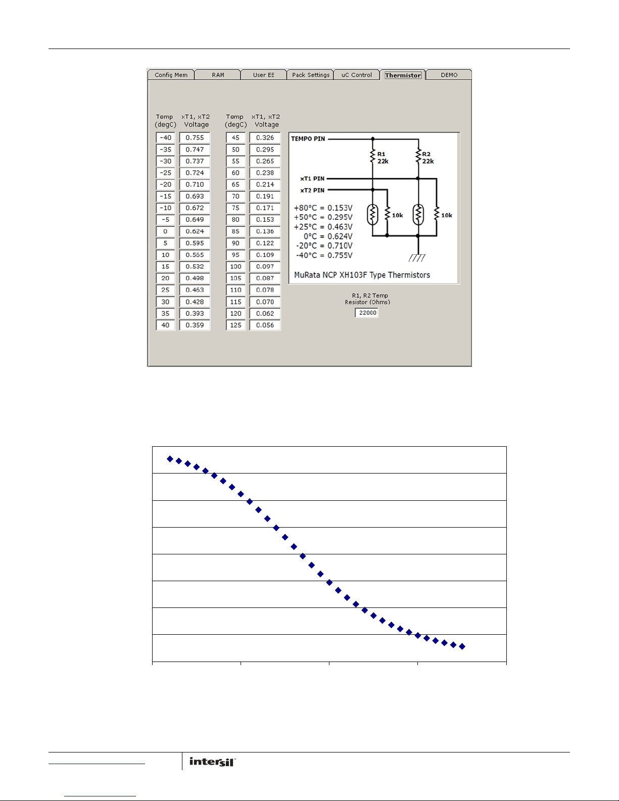
Next, the conversion depends on the external resistor divider, and
assumes that the external circuit is implemented as shown in the
Thermistor tab drawing, Figure 9 on page 8
.
There is a 10k resistor parallel to the thermistor. There are two
reasons for this. First, it makes the conversion curve more linear.
Second, the thermistor voltage range better matches the default
2x gain on the temperature input amplifier. The thermistors are
from Murata (XH103F). If an external thermistor replaces the
thermistors on the board, the conversion can be changed by
changing the values in the Thermistor tab of the GUI. The values
in the table are the voltages applied to the xTn input pins. The
voltage depends on the resistance of the Thermistor at each
temperature and the voltage on the TEMPCO pin. The TEMPCO
voltage is 2.5V.
Based on calculations, the voltage/temperature curve for this circuit
is shown in Figure 10 on page 8
. The GUI uses the Thermistor table
for this conversion and performs a linear interpolation between
points.
For calculations of the external temperature, the Thermistor tab
contains a value for the external divider resistor. This can be
changed by the user, but not saved.
Submit Document Feedback
7
AN1952.1
July 30, 2015
Page 8
Application Note 1952
FIGURE 10. VOLTAGE TO TEMPERATURE CONVERSION
0.000
0.100
0.200
0.300
0.400
0.500
0.600
0.700
0.800
-50 0 50 100 150
TEMPERATURE (°C)
INPUT VOLTAGE (V)
FIGURE 9. ISL94203 GUI THERMISTOR TAB
Submit Document Feedback
8
AN1952.1
July 30, 2015
Page 9
Application Note 1952
FIGURE 11. CURRENT READOUT
FIGURE 12. STATUS INDICATORS
FIGURE 13. FET INDICATORS
FIGURE 14. I2C ADDRESS BOX
CURRENT READINGS
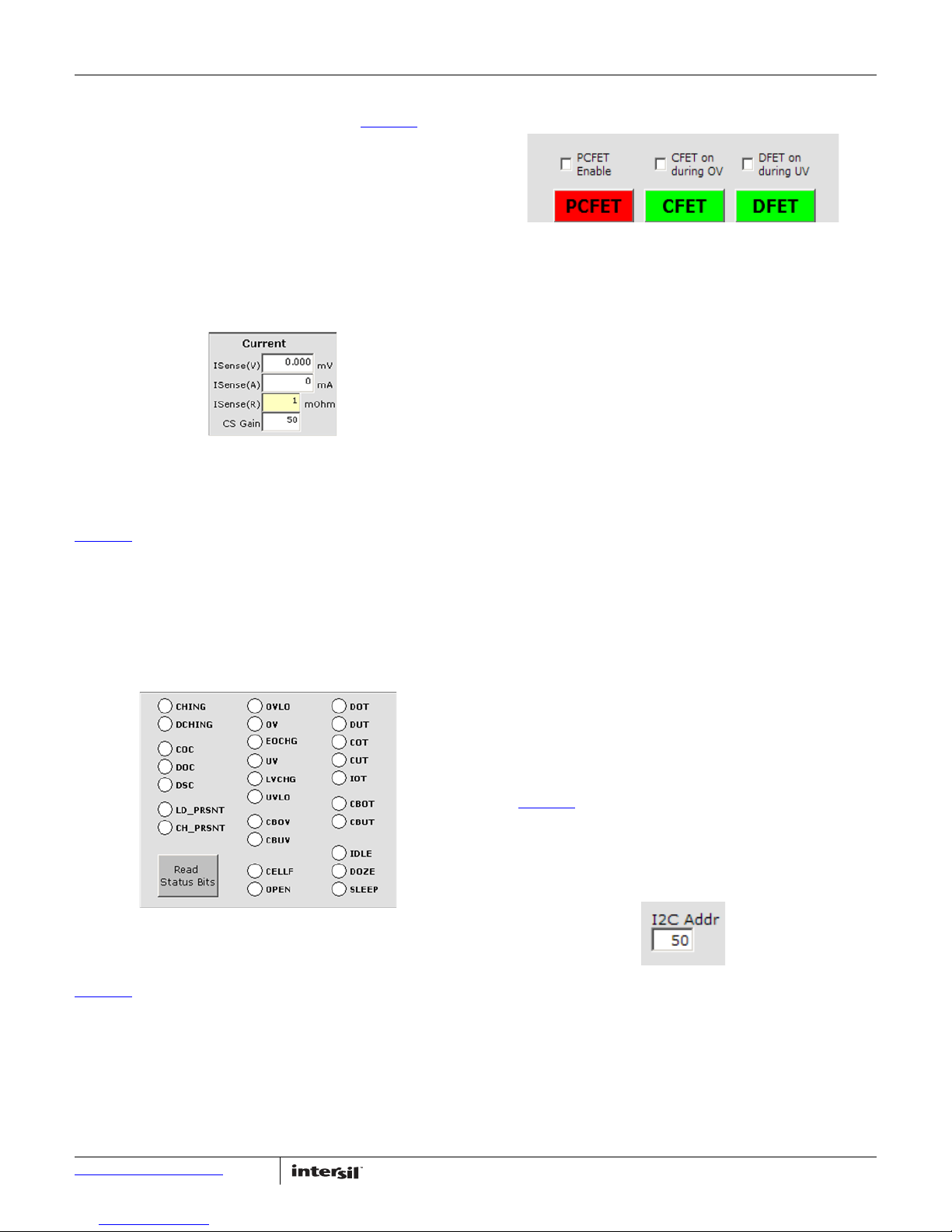
The current readout consists of four boxes, (see Figure 11). The
top box shows the voltage across the sense resistor, as reported
by the device and converted to volts. The next box shows the
current reading in milliamps. This value depends on the value of
the current resistor. This can be entered into the third current
box. The default value is 1Ω, because that is the value on the
ISL94203EVKIT1Z board. If the resistor value changes, then this
value can be changed in the GUI (but the default cannot be
changed in this revision of the GUI). The bottom box simply
relates the current amplifier gain setting in the device. In
automatic scans, there is an automatic gain control. The gain
setting is most useful when forcing a current read by the GUI.
STATUS BITS
The status indicators on the lower right of the GUI screen (see
Figure 12
indicator is red, it shows a fault or out-of-bounds condition. If an
indicator is green, it is showing an operating condition, such as
current direction or power mode.
The status indicators are automatically updated when doing a
voltage read operation. However, refreshing only the status bits is
much quicker. So, clicking the “Read Status bits” updates only
the status.
), reflect the status of the bits in the device. If an
the indicator is green. If the bit is “0” indicating that the FET
should be off, then the indicator is red.
The FET indicators are more than just readouts. Clicking on the
indicators can also set or clear the bits to turn on or turn off the
FETs. However, the GUI does not have control over the FETs when
the device is operating in stand-alone mode. To control the FETs
through the GUI requires that the µCFET bit is set first. This bit is
set or reset using the “µC Controls FET” button in the µC Control
Tab.
Above the FET control bits are some controls to change the
operation of the device. These controls are “PCFET enable”,
“CFET on during OV”, and “DFET on during UV”.
Setting the “PCFET enable” to active causes the PCFET to turn on,
instead of the CFET, when the voltage is below the Low V Charge
threshold voltage (see the Pack settings).
Setting the “CFET on during OV” to active means that the charge
FET will turn on when there is an overvoltage condition, if the
device detects a discharge current. This reduces heat generated
in the CFET during discharge. This is more important when there
is a single charge/discharge path configuration.
Similarly, setting the DFET on during UV to active means that the
discharge FET will turn on when there is an undervoltage
condition, if the device detects a charge current. This reduces
heat generated in the DFET during charge. This is more
important when there is a single charge/discharge path
configuration.
FET INDICATORS
Above the voltage readings are the FET indicators, (see
Figure 13
control bits. If the bit is “1” indicating that the FET should be on,
Submit Document Feedback
). These show the status of the PCFET, CFET, and DFET
9
OTHER MAIN SCREEN CONTROLS
Communication to the device requires an I2C bus. The I2C bus
uses a Slave byte to determine the specific device on bus that is
being addressed. In the GUI this is set by the I
(see Figure 14
). This is located in the lower left of the screen. By
default, the Slave Byte is 50H (0101 000x). This addresses the
device having the ADDR pin pulled low. In a cascade
configuration (or an application that does not need current sense
or FET control, where the ADDR pin is tied high,) write the I2C
Addr as 52.
2
C Addr box,
AN1952.1
July 30, 2015
Page 10
Application Note 1952
FIGURE 15. TEMPERATURE MEASUREMENT OPTIONS
FIGURE 16. MEMORY ACCESS
ISL94203EVKIT1Z
FIGURE 18.
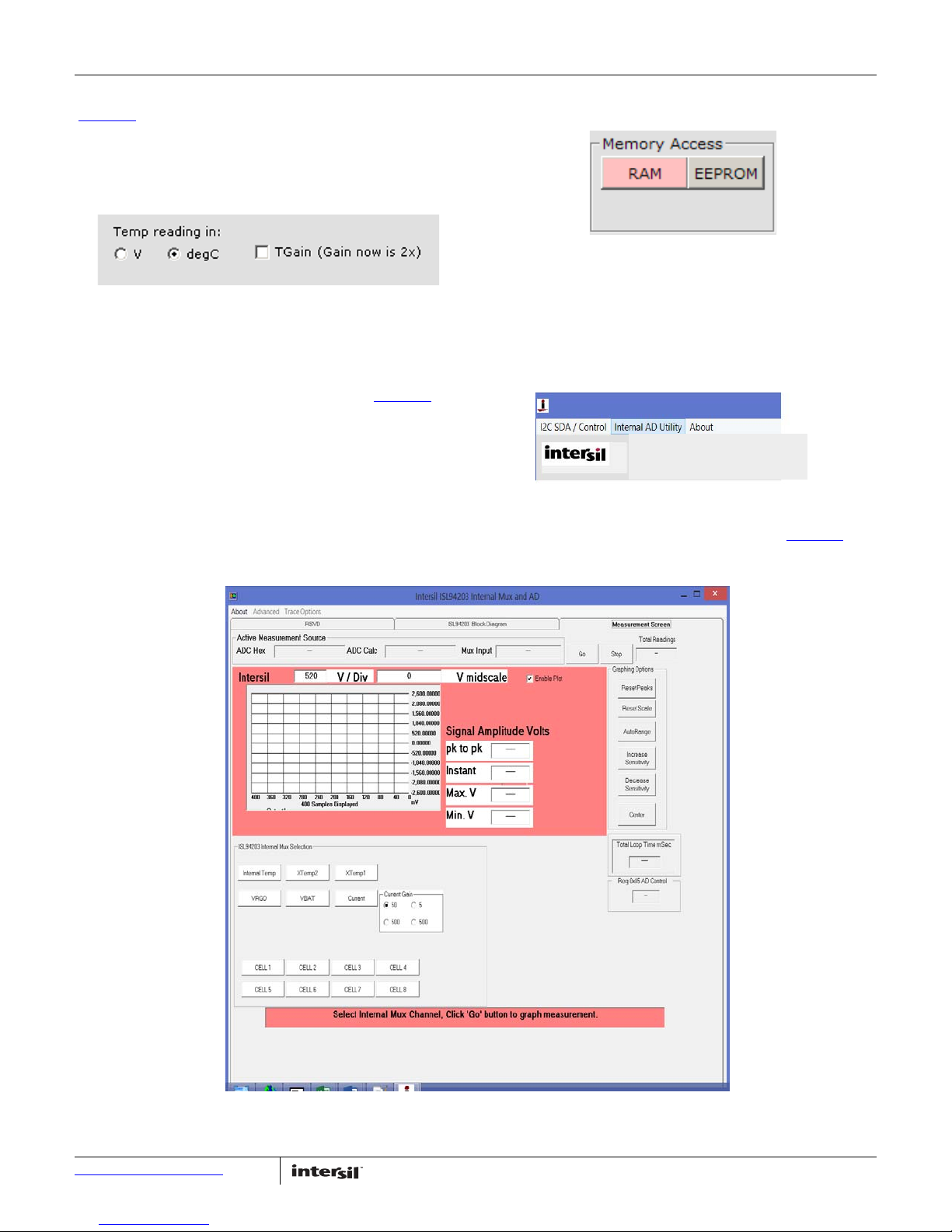
Temperature measurement options are selected in this box
(Figure 15) below the tabs. The pack settings and temperature
outputs can be shown as either volts or °C. Changing the setting
initiates a voltage scan and an update of the Pack Settings. The
calculations are made in the GUI as described in previous. The
device simply maintains the voltage value associated with the
temperature.
This box also has the selection for the TGAIN bit. Clicking on the
TGAIN box changes the TGAIN bit in the device, updates all of the
RAM settings for temperature limits and initiates an update of
the Pack Settings tab. It does not do a voltage scan. The caption
shows the current status of the temperature gain. Figure 15
indicates that the temperature gain is set to 2x.
Access to EEPROM requires an access control bit to be set prior
to a read or write operation. In all of the screens where a button
initiates multiple read or write operations, the memory access is
automatically set to the correct access code and automatically
reverts to RAM access. However, for individual memory read or
write, it may be necessary to change the access code. These
buttons allow this access code change. Simply click on the
desired memory area button, prior to the actual read or write
operation.
The ISL94203 Internal AD Utility screen enables the user to view
and record AD readings in real time. By using the I
2
C interface,
the GUI enables a user to select any of the internal Mux channels
and view/capture the results in real time.
To bring up th e AD f orm, clic k on the “Internal AD Utility”
selection on the menu bar of the main form.
FIGURE 17.
When first loaded, the new form will appear as in Figure 18
.
Submit Document Feedback
10
AN1952.1
July 30, 2015
Page 11
Application Note 1952
FIGURE 22.
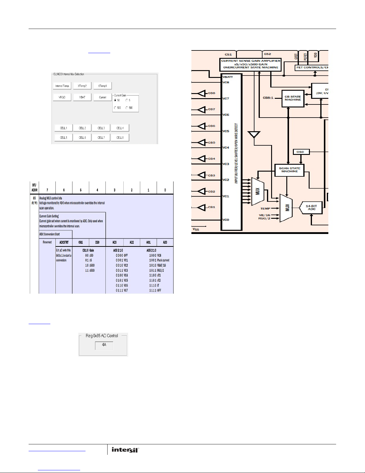
An important first step is to select an internal Mux Channel that
is going to be measured. By making a selection (clicking on a
Mux selection button, see Figure 19), data collection/graphing
will automatically start and after a few seconds “Auto Range” will
take place.
FIGURE 19.
Essentially, clicking in the frame selection selects the value
written to register 0x85. The user can consult the data sheet for
specifics related to each Mux Input connection.
Therefore, this selection programs the “MUX” blocks connected
to the input of the internal AD.
FIGURE 20.
A real-time display of the register contents is displayed in
Figure 21
Submit Document Feedback
.
FIGURE 21.
11
AN1952.1
July 30, 2015
Page 12
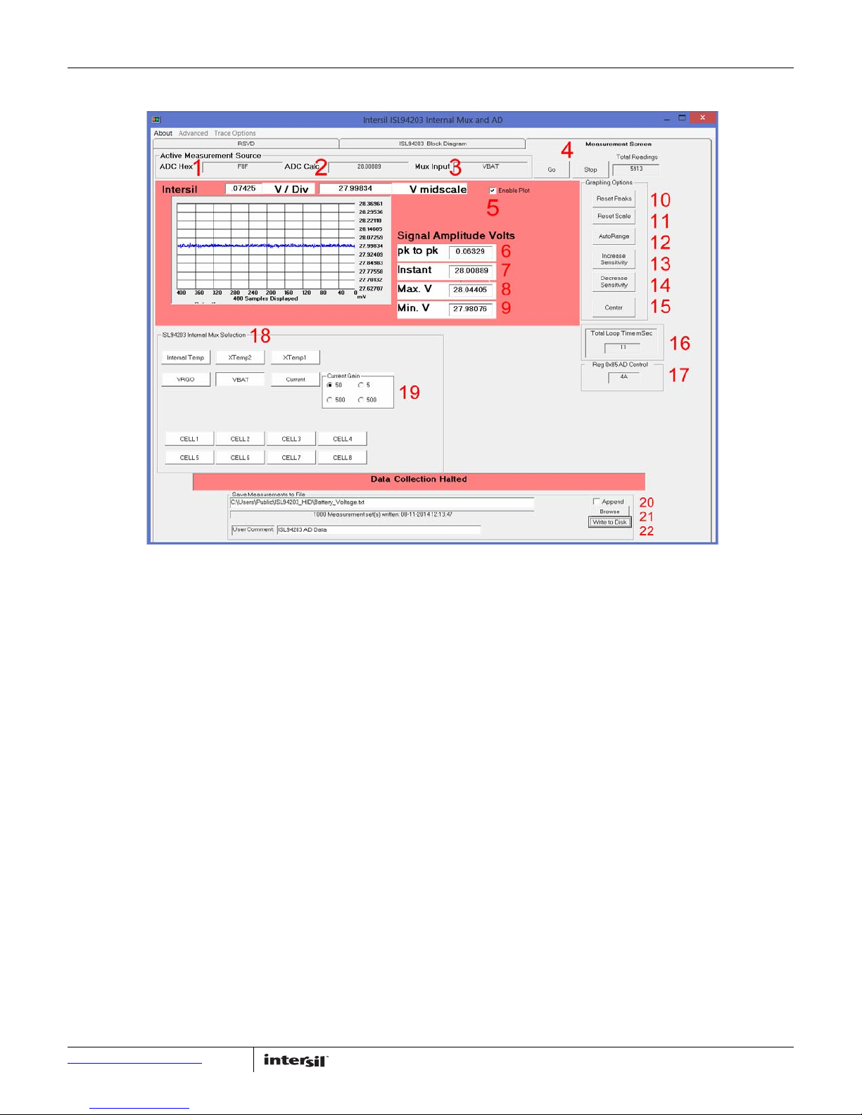
MAIN AD FORM TOOLS
FIGURE 23.
Application Note 1952
1. Actual Dual Byte Hex value of AD reading
2. Calculated value based on channel selected
3. Active channel being measured
4. GO Starts and STOP ends data collection. Click “Stop” to save
collected readings to file.
5. Enable Plot, speeds up data collection by disabling real-time
graphing
6. Highest reading – lowest reading
7. Display of most recent reading
8. Peak/Maximum value recorded
9. Minimum value recorded
10. Clears items 6, 8, 9
11. Resets graphing scale to max default
12. Recalculate Maximum and Minimum values of graphing area
13. Decreases volts per division (visual only does not affect
collected readings)
14. Increase voltages per division (visual only does not affect
collected readings)
15. Recenters midrange scale and moves graphing range
16. Actual time in milliseconds to capture and graph a
measurement
17. Hex value of Mux control register
18. Internal Mux selection
19. PGA gain selected when making a current measurement
20. Checking will append latest collection of readings to a file
21. Browse to directory location where captured readings will be
saved
22. Perform actual write operation
Submit Document Feedback
12
AN1952.1
July 30, 2015
Page 13
Application Note 1952
FIGURE 24.
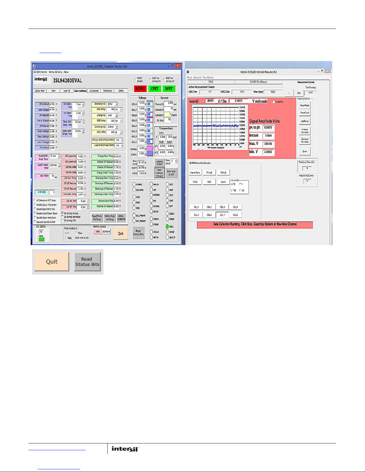
To quit the program, click on “Quit”.
The Internal AD Utility form is a separated form that can be
closed or minimized independent of the main screen
(see Figure 24).
Submit Document Feedback
13
AN1952.1
July 30, 2015
Page 14
Application Note 1952
Tab Controls
ISL94203 Memory Access
RAM
The ISL94203 has two main memory areas, RAM and
Configuration Memory. The RAM area contains the transient
values, such as cell voltages, status bits and microcontroller
override conditions. The RAM registers relate to the part of the
GUI already described and the GUI reads and writes these
registers as needed. The user also has direct access to the RAM
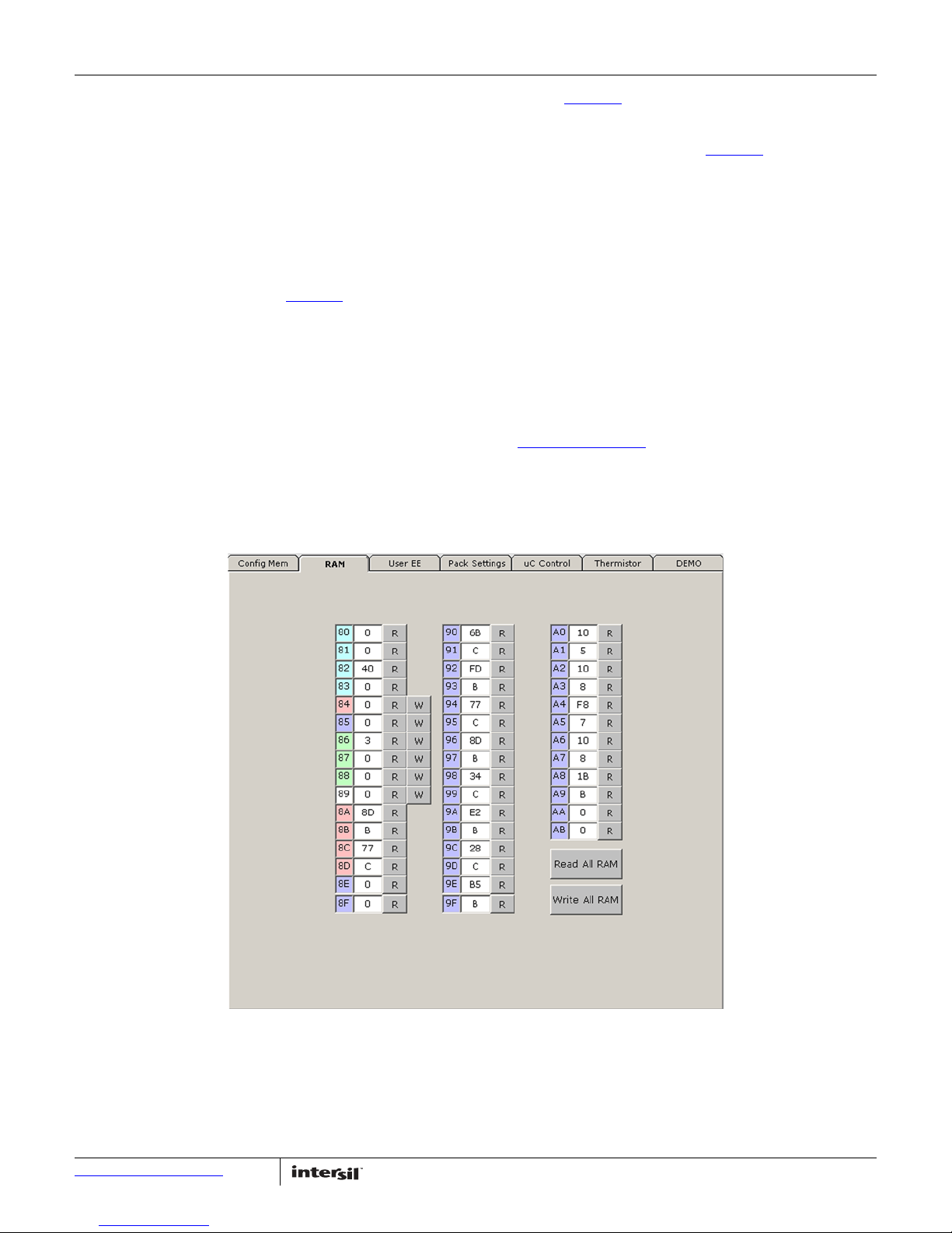
memory through the RAM tab. See Figure 25
To update the values in the GUI with the values in the ISL94203,
press the “Read All RAM” button. The display now shows the hex
values of the RAM registers. Alternatively, each individual
location can be updated by clicking on the “R” to the right of the
register location.
There are only six registers that can be changed by the user.
These are addresses 84H to 89H. These locations have a “W”
next to the register. To change the register contents, write a new
hex value in the desired location and press the “W” button (or the
“Write All RAM” button). Until a write occurs, the contents of the
ISL94203 RAM is not changed.
.
As shown in Figure 25
address of a register returns a description of the register. Also,
the registers are color coded to match the datasheet and to
group like registers. For example, in Figure 25
84H are cyan color. These are the status registers. Also, registers
8EH through ABH are blue. These registers hold the voltage
readings for the cells, current and temperature.
When pressing the “Read All RAM” or “Write All RAM” buttons,
the color of the button changes and the caption changes to
“Busy”. During this time the GUI is performing the specified
operation and other operations are prohibited until the read or
write completes and the color and caption return to normal. This
sequence occurs on all controls described in the following.
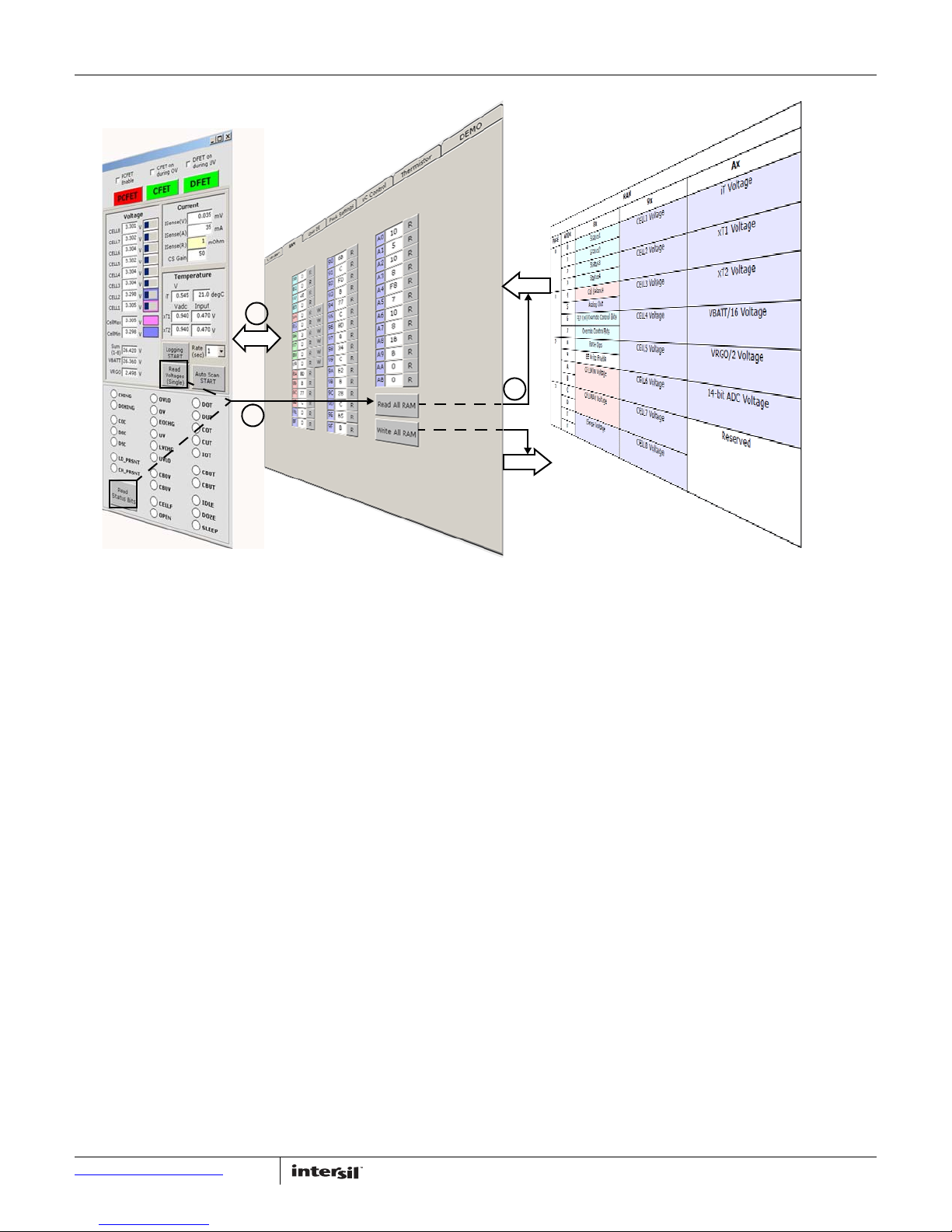
The main screen shows the “real world” contents of the
ISL94203 registers, converting hex values to volts, current, or
temperature and indicating individual status bits. The GUI
performs this update when the “Read Voltages (Single)” or
automatic scan executes. The update operation begins with a
Read All RAM operation. This brings in values from the ISL94203
(see Figure 26 on page 15
in RAM to the proper voltage, current, or temperature value.
The GUI controls for the writable RAM registers are located in the
µC Control tab. These tab operations will be discussed in more
detail in the following.
, hovering the mouse pointer over the
, registers 80H to
). The GUI then converts the hex values
Submit Document Feedback
14
FIGURE 25. ISL94203 GUI RAM ACCESS TAB
AN1952.1
July 30, 2015
Page 15
Application Note 1952
ISL94203
RAM MEMORY
ISL94203
GUI RAM TAB
ISL94203
MAIN SCREEN
FIGURE 26. ISL94203 GUI RAM UPDATE OPERATION (READ OPERATION NUMBERED)
2
3
1
NOTE: “Read Voltages (Single)” or “Read Status Bits” Operation execution steps are numbered. “Write All RAM” writes to the ISL94203 RAM memory,
then updates the Main Screen.
Submit Document Feedback
15
AN1952.1
July 30, 2015
Page 16
Application Note 1952
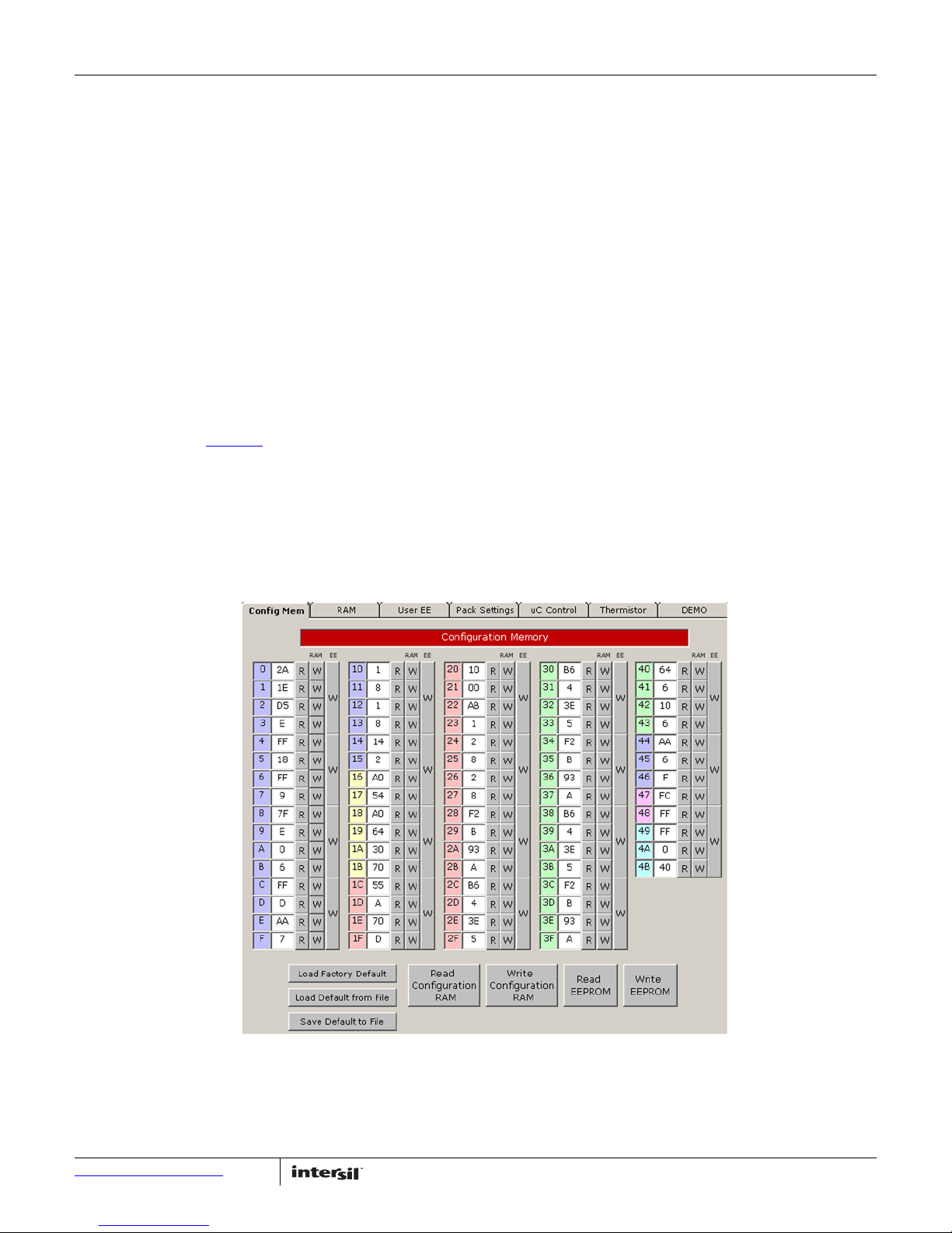
FIGURE 27. ISL94203 GUI - EEPROM ACCESS TAB
CONFIGURATION MEMORY
The Configuration Memory consists of two parts, the EEPROM
cells and Configuration RAM. On power-up, the contents of the
EEPROM is copied to the Configuration RAM. The device operates
out of Configuration RAM.
Reading and writing the EEPROM does not automatically go
through the Configuration RAM. Writes made to the EEPROM
locations will go into effect when the device power cycles or
when the EEPROM contents are read from the EEPROM and
rewritten to the Configuration RAM.
In the normal course of developing an application, a change is
made to the Configuration RAM. This changes the operation of
the device. For example, changing the overvoltage setting in the
Configuration RAM changes the voltage at which the device
detects a fault condition. However, the value has not yet changed
in the EEPROM, so a power cycle returns the old OV threshold. To
make the value permanent requires that the value also be
written to the EEPROM.
The EEPROM tab (see Figure 27
registers. This could be the values read from the Configuration
RAM or from the EEPROM. Which values it displays is dependent
on the access code. The access code is set in Register 89H, but
the GUI automatically sets this bit when the “Read EEPROM” or
“Write EEPROM” buttons are pressed. The Access code is also
settable by clicking the Memory Access button as described
previously.
) of the GUI shows only one set of
To write to individual bytes of the RAM part of the Configuration
Memory, set the “RAM Access” in the Memory access box. Each
byte in RAM can be written separately.
Writing to individual bytes to the EEPROM part of the
Configuration Memory is limited. Each EEPROM write needs to
write all four bytes on a page. For this reason, the GUI has a
different (larger) button for writing to EEPROM. As previously
mentioned, in order to write to a page of EEPROM, it is necessary
to set the “EEPROM Access” in the Memory access box prior to
the write.
As with the RAM tab, hovering over an address box brings up a
dialog showing a simple description of the register contents.
Also, the various registers are color coded as shown in the
datasheet and are grouped by function.
The EEPROM tab has three other buttons. The first is a “Load
Factory Default” button. This fills the GUI EEPROM locations with
the factory default values (as defined at the time of the GUI
release). This lets a user recover to a known good operating
point. Again, use of this button simply fills the GUI registers. To
change the operation of the device or the contents of the
EEPROM requires a separate write for each memory location.
The other two buttons are “Save User Default to File” and “Load
User Default from File.” These commands allow the user
Configuration Memory to be saved and recalled. The values
saved are locations 0H through 4BH.
Submit Document Feedback
16
AN1952.1
July 30, 2015
Page 17
Application Note 1952
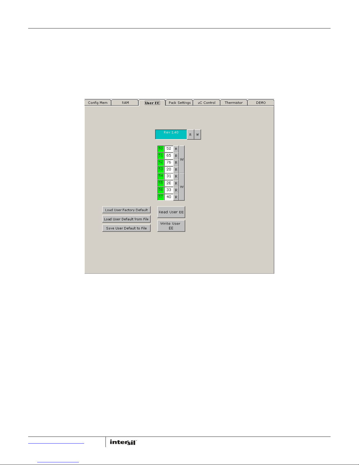
FIGURE 28. ISL94203 GUI - USER EEPROM TAB
USER MEMORY
The user memory area is different from the Configuration
memory. The User memory does not have a RAM component, so
all reads and writes are to the EEPROM only. Also, the device
ships with the user memory cleared. So, an initial read from user
memory reads 0.
Using the Load User Factory Default tells the GUI to put the
software revision number in the GUI locations for the user
memory. The user can keep these values or load other data in
the GUI boxes. To write the data to the ISL94203 User EEPROM
requires individual writes (click the “EEPROM Memory Access”
first) or a write all, using the “Write User EE” button (this
automatically sets the EEPROM Access bit).
The User EE tab also includes a Load Default from File and a
Save User Default to File. These buttons load and save User EE
data at addresses 50H to 57H only.
Submit Document Feedback
17
AN1952.1
July 30, 2015
Page 18
Application Note 1952
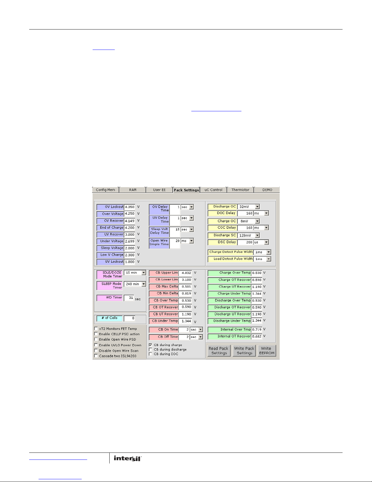
FIGURE 29. ISL94203 GUI - PACK SETTINGS TAB
PACK SETTINGS TAB
The Pack Settings tab (see Figure 29) provides access to the
contents of the Configuration RAM, but with “real world” values.
This provides an easier way to program the operation of the pack
and to monitor the present settings. Values in the Pack Settings
tab are saved in the GUI. When a “Read Pack Settings” button is
pressed, the value is read from the device and loaded into the
Configuration RAM tab of the GUI. The GUI then takes the
contents of the Configuration RAM, calculates the real world
value and writes it to the pack settings tab.
When a value is changed in the Pack Settings tab, nothing
happens until a “Write Pack Settings” button is pressed. The GUI
then takes the value in the Pack Settings tab, converts the value
to hex and writes the new value to the Configuration RAM tab in
the GUI. These values are then written from the GUI to the RAM
part of the device Configuration memory. If a value is changed in
the GUI, but no write button is pressed, then the device is not
updated with the new value.
As soon as the Write Pack operation completes, the ISL94203
begins operating with the new parameters.
The Pack Settings tab also includes a “Write EEPROM” button.
This is a convenience, since it does the same function as the
button in the EEPROM Tab. However, in the Pack Settings tab, it
is necessary to do a “Write Pack Settings” operation prior to
doing the “Write EEPROM”. Otherwise, the EEPROM would not
get the latest values from the Configuration Memory RAM to
write to EEPROM. This is because the “Write EEPROM” writes
values from the GUI Config Mem tab to the device and the values
in the GUI Config Mem tab are not updated until execution of the
“Write Pack Settings” operation.
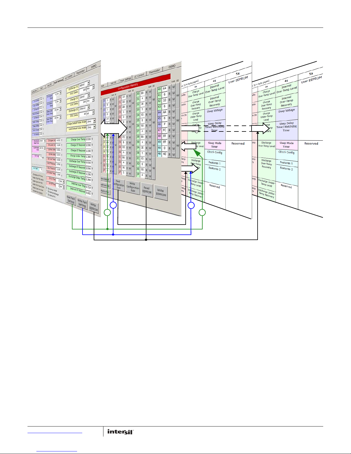
Figure 30 on page 19
shows a graphical representation of the
operation of the Pack Settings tab operation, the GUI EEPROM
tab and the ISL94203 internal registers.
The memory operations of the Pack Settings tab was described
above. The next section covers some additional details about the
calculations and use of the values shown in the Pack Settings
tab.
Submit Document Feedback
18
AN1952.1
July 30, 2015
Page 19
Application Note 1952
(NO USER
SHADOW
RAM)
COPY
COPY
COPY
ISL94203 DEVICE
CONFIGURATION RAM
ISL94203 DEVICE
EEPROM MEMORY
(EEPROM SHADOW MEMORY)
ISL94203 GUI
EEPROM TAB
ISL94203 GUI
PACK SETTINGS TAB
FIGURE 30. ISL94203 GUI PACK SETTINGS TAB MEMORY OPERATIONS
2
1
TRANSLATE
1
2
Submit Document Feedback
19
AN1952.1
July 30, 2015
Page 20
Application Note 1952
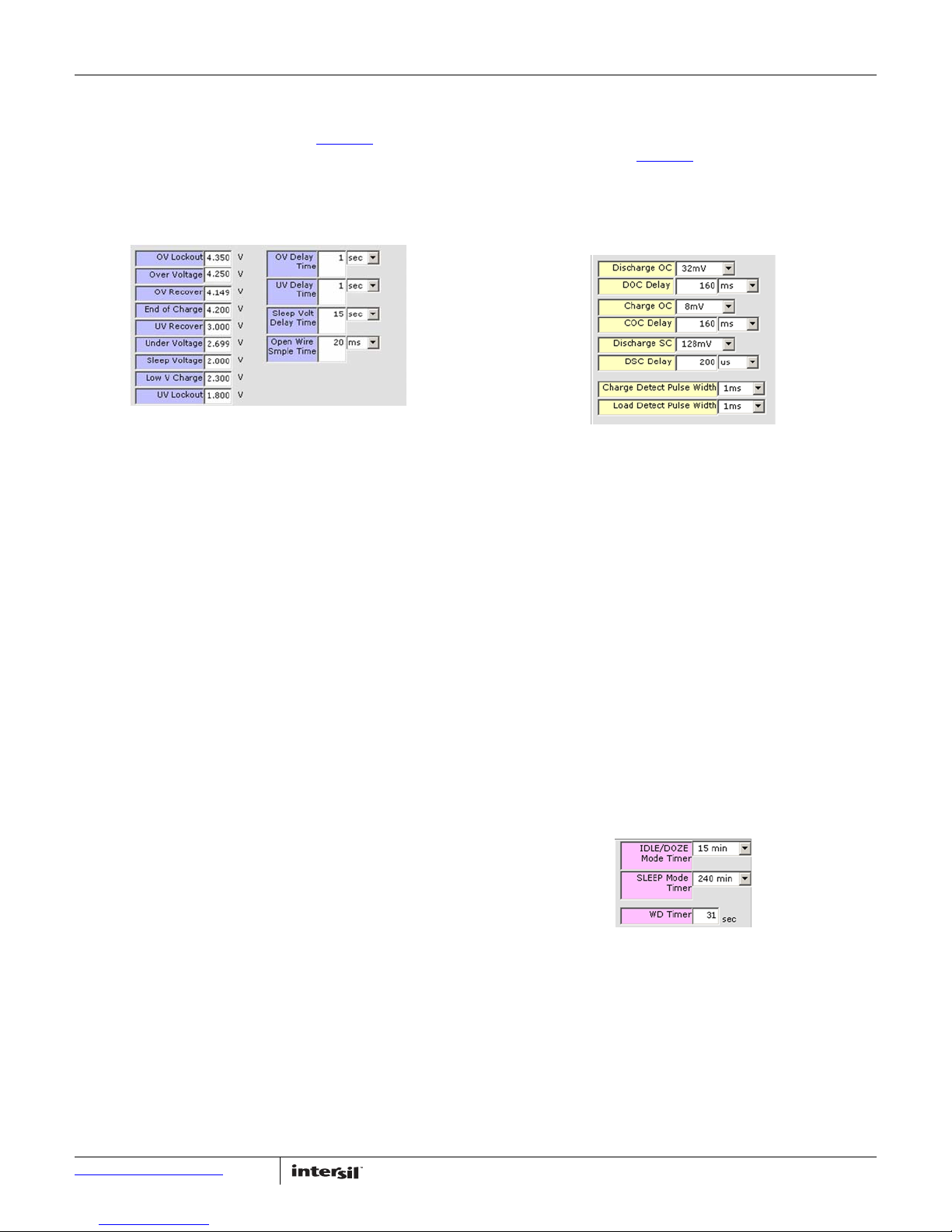
FIGURE 31. VOLTAGE THRESHOLDS AND DELAY TIMES
FIGURE 32. CURRENT LIMITS
FIGURE 33. TIMER CONTROLS
VOLTAGE LIMITS
The upper left section of the Pack Settings tab contains the
voltage thresholds and delay times, (see Figure 31). The voltages
can be set from 0V to 4.8V. A negative number loads 0 and a
value greater than 4.8V loads 4.8V. The timer values for OV Delay,
UV Delay, and Open Wire Sample Time can be between 0 and
1023. The timer value for Sleep Voltage Delay time can be
between 0 and 512.
Normally, the OV Lockout threshold is greater than the
Overvoltage threshold and the UV Lockout threshold is lower than
the Undervoltage threshold. The reason for this is based on the
definition of the values. Reaching the overvoltage and
undervoltage thresholds causes the respective power FETs to
turn off, but the pack continues to operate normally. However, if
the voltage of any cell reaches the UVLO or OVLO thresholds, then
something is very wrong with the pack or the charger. Reaching
the OVLO threshold causes the device to set a pack shutdown
(PSD) bit. This can be used to blow a fuse to disable the pack.
Reaching the UVLO threshold indicates that one or more cells are
much below their lower limit, so the device powers down to
remove as much load as possible from the cells.
The End of Charge threshold is usually lower than the overvoltage
threshold. When a cell reaches the overvoltage threshold, the
end of charge output (EOC pin) can turn off the charger. If the
voltage continues to rise, then there is something wrong with the
charger, so the overvoltage indication turns off the charger
current from within the pack.
Alternatively, the EOC limit can be used for cell balancing to
specify a level where balancing is to begin. In this case, when any
cell reaches the End of Charge threshold, all cells that are higher
than CELLMIN + CB MIN Delta start to balance. Balancing
continues until all cells are below the EOC Threshold -117mV.
CURRENT LIMITS
To the right of the voltage settings are the current limits for
discharge overcurrent, charge overcurrent, and discharge
short-circuit events, (see Figure 32). The delay time values can be
0 to 1023 microseconds, milliseconds, seconds or minutes. Care
should be taken when setting the range of these timers. The
threshold levels are set by drop down boxes and set the
overcurrent level by setting the voltage expected across the
sense resistor.
Also in this selection is the setting for the duration of the charge
and load pulse widths. When the power FETs turn off in response
to an overcurrent event, the ISL94203 starts looking for the
release of the load or charger. It does this by periodically
sourcing or sinking a current to the load or from the charger. The
duration of the pulse width might need to be changed, depending
on the load or charger capacitance, since the detection circuit is
attempting to pull the voltage at the terminals to some
intermediate state. If the load or charger is off, but there is a
large capacitance still connected to the terminals, a short pulse
width will take longer to detect the removal. The ISL94203
allows detection pulse widths from 1ms to 16ms.
TIMERS
Below the voltage settings are some timer controls. The upper
box specifies the amount of time the device spends in normal
mode (with no measured current) before entering into IDLE and
the time the device spends in IDLE before entering the DOZE
mode. The Sleep Mode timer specifies how long the device
remains in DOZE mode (with no measured current) before going
to sleep. Detection of any current returns the part to the normal
operating mode.
The Sleep voltage, along with the sleep voltage timer determine
if the cells drop below a sleep threshold. If so, the power FETs
turn off and the device enters a sleep mode. The device wakes
from a sleep mode by the connection of a load or a charger to the
pack.
The “Low V Charge” threshold is used when the Precharge FET is
enabled. The low voltage charge threshold is the level where the
charge FET turns on instead of the precharge FET. When the cell
voltages are below the Low V charge level, the precharge FET is
on. When the cell voltages are greater than the Low V charge
level, then the charge FET is on.
Submit Document Feedback
20
The WD Timer setting is used with µC override operations. When
the µC sets any condition that overrides internal operation, the
WD timer starts. The WDT is reset by any valid reception of an I
2
slave byte. If there are no valid communications before the WDT
times out, then the ISL94203 turns off all FETs and waits for a
valid command.
AN1952.1
July 30, 2015
C
Page 21
Application Note 1952
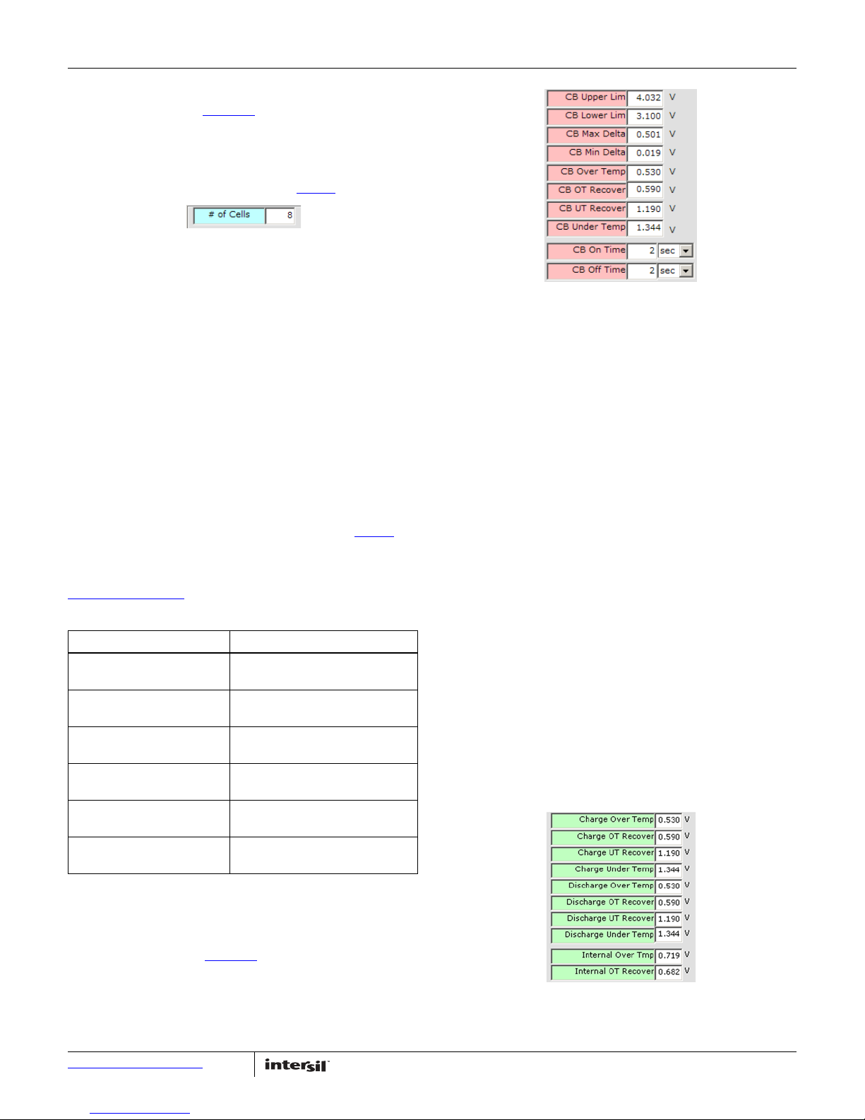
FIGURE 34. NUMBER OF CELLS BOX
FIGURE 35. NUMBER OF CELLS BOX
FIGURE 36. PACK TEMPERATURE LIMIT SETTINGS
NUMBER OF CELLS
The number of cells box (Figure 34) specifies the number of cells
connected to the pack. The number in the box can be lower than
the number of cells connected to the pack. This value is a direct
representation of the number of cells, it is not the value stored in
memory. The GUI translates the number of cells value to the
proper code for the device, as specified in Table 1
When the board first powers up, the “# of Cells” is set to 3. This
causes some of the cells to show 0V in a Voltage Scan. This is
because the cells are skipped in the scan. If there are more cells
connected, change the setting, write the values to the pack, then
write the values to EEPROM.
The reason for the default value of 3 in the # of Cells box is that,
if the number in the box is greater than the number of cells
connected to the pack, when the ISL94203 first powers up it
reads a cell input as 0V. The ISL94203 thinks that this is a cell
failure, so does not complete its power up sequence. This is part
of the protection mechanisms of the part. If the value written to
the EEPROM is higher than the number of cells connected and
the device powers down, then it will not power up properly. It will
be necessary to connect the programmed number of cells (or
more) so the device powers up. Then the EEPROM value can be
reset.
For the proper connections of fewer than 8 cells, see Table 1
When using the evaluation board with fewer than 8 cells, connect
the unused cell inputs at the board connection. It is not
necessary to remove any components on the board (see
Figure 55 on page 31
TABLE 1. ISL94203 CELL CONFIGURATION
CELLS VALUE NUMBER OF CELLS
1 0 0 0 0 0 1 1 3 Cells connected,
1 1 0 0 0 0 1 1 4 Cells connected,
1 1 0 0 0 1 1 1 5 Cells connected,
1 1 1 0 0 1 1 1 6 Cells connected,
1 1 1 0 1 1 1 1 7 Cells connected,
1 1 1 1 1 1 1 1 8 Cells connected,
NOTE: Only these combinations are acceptable. Any other combination
will prevent any FET from turning on.
).
C1, C2, C7, C8
C1, C2, C3, C7, C8
C1, C2, C3, C6, C7, C8
C1, C2, C3, C4, C6, C7, C8
All cells connected
.
.
C1, C2, C8
The CB lower limit and CB upper limit define the boundaries of
the cell voltage operation (except in EOC balancing). If ALL cell
voltages exceed the limits, then balancing stops. Balancing starts
again when ALL cell voltages drop back within the specified
limits plus a hysteresis. For example, if the CB upper limit is set
to 4.0V, then balancing stops when all cell voltages exceed 4.0V.
Balancing resumes when all cell voltages drop below 3.883V.
CB Max Delta specifies the maximum difference between the
CELLMAX and CELLMIN values. When this happens, it implies
that there is something wrong with the cells or connections.
When cell voltages exceed the CB Max Delta limits, the CELLF
flag is set. This can cause the PSD pin to active (optional) which
can shut down the pack. The CELLF indication also starts the
open wire detection operation.
The CB over- and under-temperature settings specify the
temperature range over which the cell balance operates. If the
external temperature sensors show that the temperature is out
of bounds, then cell balance stops.
The CBON and CBOFF times specify how long the cell balance is
on and off. These timers are mainly used for thermal control to
manage the heat dissipated by the cell balance resistors.
TEMPERATURE LIMITS
On the lower right of the Pack Settings tab are the pack
temperature limit settings. There are temperature limits for
charge and discharge as well as temperature recovery levels for
each. These limits refer to the ADC converted value of the
temperature sensor inputs, so they are affected by the TGAIN bit.
The GUI limits values in these locations from 0 to 1.8V (voltage
setting) or -40°C to +125°C (temperature setting).
CELL BALANCE LIMITS
The next box to the right (Figure 35) contains the settings for cell
balancing. The voltage limits that can be set in the GUI are fixed
at 0 and 4.8V. There are no limits to the temperature settings.
The temperature values are limited by the GUI from 0 to 1.8V
(voltage setting) or -40°C to +125°C (temperature setting).
Submit Document Feedback
21
AN1952.1
July 30, 2015
Page 22

Application Note 1952
FIGURE 37. OPTION CONTROLS
FIGURE 38. CELL BALANCE CONTROLS
When the TGAIN bit changes from “0” to “1” or “1” to “0”, the GUI
rewrites the values of the temperature limits in the EEPROM tab
(based on the temperature input amplifier gain) and sends these
new values to the ISL94203. The GUI also updates the Pack
Settings Information. The Pack Settings tab temperature limits
do not change if they are shown in °C, but the value in the device
does change. This is because the calculations for the
temperature settings in °C includes the setting of the TGAIN bit.
PACK OPTIONS
In the lower left of the Pack Setting tab are various option
controls (see Figure 37).
Setting the “xT2 Monitors FET Temp” to “1” tells the device to
treat the xT2 input as a FET temperature, not a cell temperature.
With this bit set, an over-temperature on the xT2 input does not
stop cell balancing, it only turns off the power FET.
The “Enable CELLF PSD action”, when set to “1”, causes the PSD
bit to be set when the device detects a condition that sets the
CELLF bit.
CELL BALANCE ENABLE
As part of the Cell balance settings are the Cell Balance controls
for charge, discharge or end-of-charge balancing (see Figure 38).
If “CB during charge” is checked, then the device activates cell
balancing if charge current is detected and all other conditions
are within limits. If there is no current or there is discharge
current, then the device does not balance.
If “CB during discharge” is checked, then the device activates cell
balancing if discharge current is detected and all other
conditions are within limits. If there is no current or there is a
charge current, then the device does not balance.
If the “CB during EOC” is checked, then the device ignores the
current detection and balances only based on the end-of-charge
condition (as long as all other conditions are with limits). With
this option selected, cell balancing is enabled when any cell
reaches the end-of-charge threshold. Balancing continues as
long as any cell is greater than the EOC threshold minus 117mV.
While cell balancing is enabled, in any mode, balancing is turned
on for any cell whose voltage is more than CELLMIN + CB Min
Delta volts.
The “Enable Open Wire PSD” bit, when set to “1”, causes the PSD
bit to be set when the device detects an open wire condition.
The “Enable UVLO Power Down”, when set to “1”, causes the
device to power down when it detects an undervoltage lockout
condition.
The “Disable Open Wire Scan” bit, when set to “1”, turns off the
open wire scan operation.
The “Cascade two ISL94203” bit, when set causes the device to
operate in cascade mode - as determined by the ADDR input.
When the ADDR input is tied to RGO, then the part thinks that it
is the lower device, so it turns off the current sense circuits and
does not drive the FETs. When the ADDR is tied to VSS, then it
thinks it is the upper device, so it keeps the current sense circuit
on and controls the power FETs. The ADDR bit also changes the
2
C slave byte address.
I
µC Control Tab
The µC Control tab provides a mechanism for the GUI to override
the internal operation of the device. An external microcontroller
would use similar techniques to provide different functionality to
the pack than is offered by the built-in automatic operations. The
options available on the µC Control tab are shown in Figure 39 on
page 23.
POWER CONTROL
The mode of operation of the device is controlled by these check
boxes (see Figure 40 on page 23
device into that mode of operation. Clicking on “None” removes
any forcing condition. The µC Control features does not allow the
device to be placed back into normal operation. For example,
once the device enters IDLE mode, it can be placed in DOZE
mode, returned to IDLE mode, put to sleep, or set to power down,
but it can only return to a normal scan operation if it detects
current flow in the pack. The GUI also offers a demo mode that
forces a current indication, so that can be used to return to
normal mode.
It is not necessary to override any internal operation to change
the operating mode.
). Clicking any box puts the
Submit Document Feedback
22
AN1952.1
July 30, 2015
Page 23
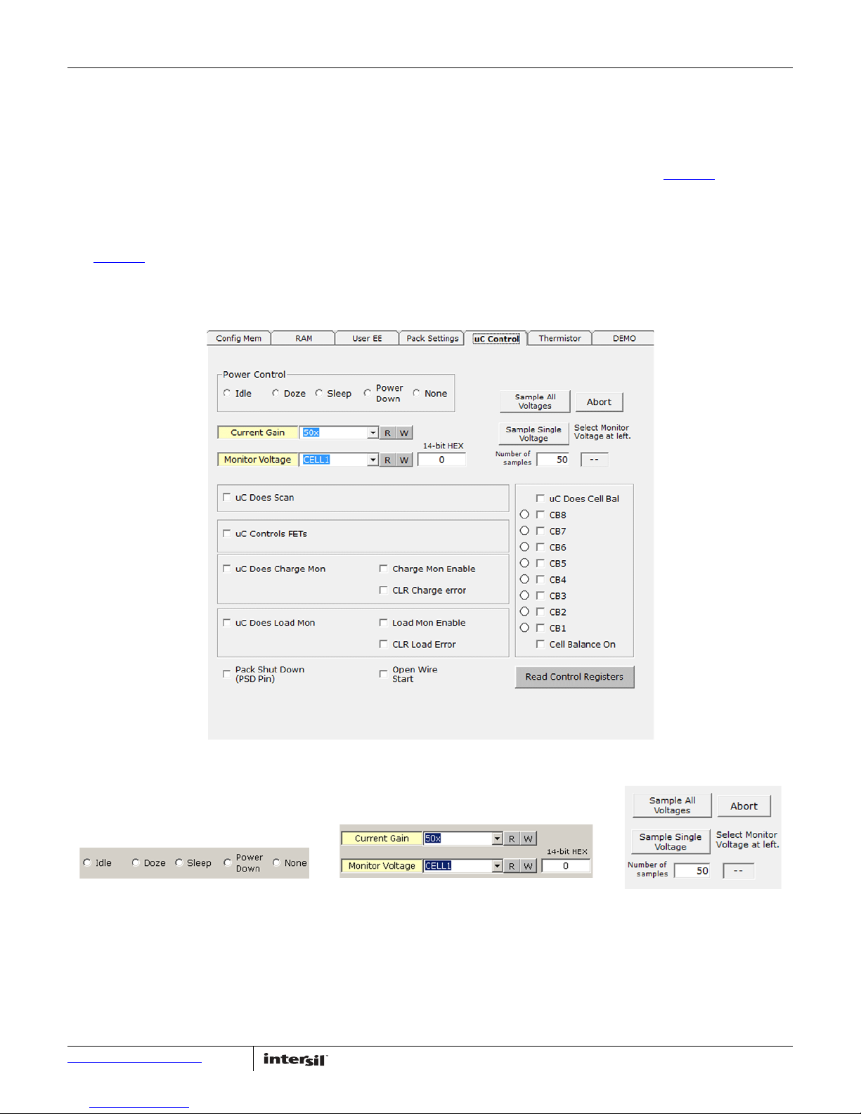
Application Note 1952
FIGURE 39. ISL94203 GUI - µC CONTROL TAB
INDIVIDUAL VOLTAGE MONITORING
The GUI or an external µC can force a read of any voltage
available from the internal MUX. This includes cell voltages, pack
current and voltage, and temperatures. It is not necessary to
override any internal function to use this measurement.
To use this feature, select the voltage to be measured and click
the “W” button. The “R” button reads the status of the AO3:AO0
bits, but a write operation sets the bits for the desired voltage
and sets the ADCSTRT bit, needed to start the internal conversion
operation. The resulting voltage shows in the box at the right,
(see Figure 41
to be converted to voltage, current or temperature.
). This is a 14-bit hex value. This value then needs
When measuring the current, the gain of the amplifier can be
manually set prior to the ADC read by using the drop down box
and “W” button on the top line.
The GUI allows the repetitive capture of any single voltage or all
voltages. For a single voltage capture, the desired voltage is
selected by the Monitor Voltage box (see Figure 42). The number
of samples is specified and the “Sample Voltages” button is
pressed. This brings up a dialog box asking for the file name for
the data to be stored. The GUI then captures the specified
number of samples and stores the data to the file. This is a tab
delimited file that can be imported into Excel.
Between the Sample All Voltages and Sample Single Voltage
buttons is a progress indicator showing the ongoing data capture.
FIGURE 40.
Submit Document Feedback
23
FIGURE 41.
FIGURE 42.
AN1952.1
July 30, 2015
Page 24
Application Note 1952
FIGURE 43.
FIGURE 44. CELL BALANCE
FIGURE 45.
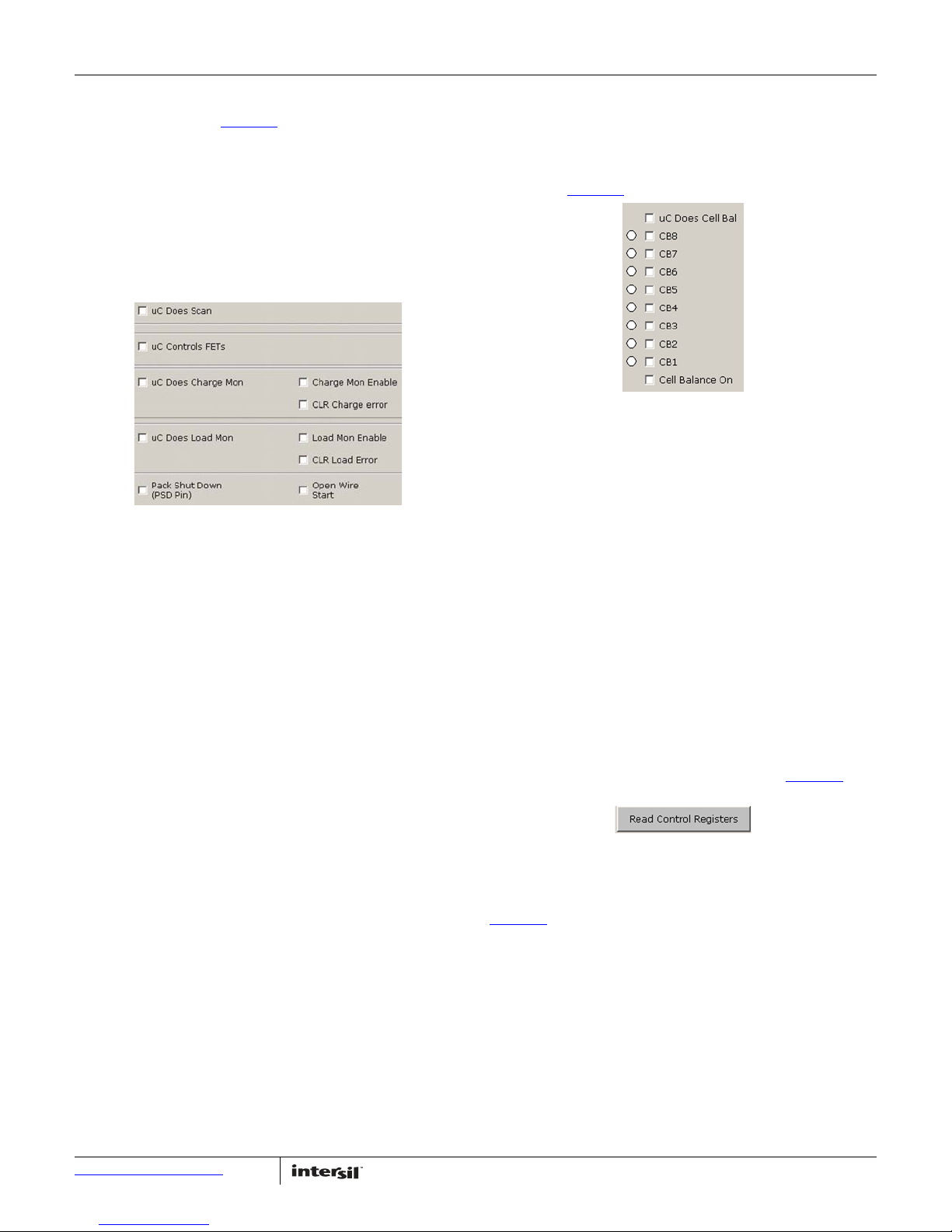
MICROCONTROLLER DOES...
The next set of controls (Figure 43) allows the GUI (or
microcontroller) to take over several functions of the device. The
most general is the “µC Does Scan” box. When checked, the
device stops scanning the cells, which effectively stops
automatic operation. When this box is checked, cell voltages are
scanned by the external µC, OV and UV voltages must be
manually compared with limits and cell balance must be
controlled externally. The only function maintained internally
during a µCSCAN operation is the overcurrent/short circuit
monitoring. These continue to be automatically monitored.
The “µC Controls FETs” operation gives the GUI or external µC
control over the FETs. With this box unchecked, the ISL94203
has exclusive control over the FETs. It is not possible to change
the FETs from the outside. When the box is checked, the FETs are
only controlled by the GUI or an external µC.
The “µC Does Charge Mon” bit overrides the internal charger
monitor function. When overridden, the GUI or an external µC can
turn on the charger monitor current and detection hardware by
setting the “Charge Mon Enable.” The GUI or external µC then
needs to monitor the CH_PRSNT bit to detect if there is a charger
present. If the charger is removed following an overcurrent
condition, then the GUI/µC needs to reset the charge error bit by
clicking on “CLR Charge Error”.
The “µC Does Load Mon” bit overrides the internal load monitor
function. When overridden, the GUI or an external µC can turn on
the load monitor current and detection hardware by setting the
“Load Mon Enable.” The GUI or external µC then needs to monitor
the LD_PRSNT bit to detect if there is a load present. If the load is
removed following an overcurrent condition, then the GUI/µC
needs to reset the load error bit by clicking on “CLR Load Error”.
All of these operations start the Watchdog timer. If
communications with the device stop for more than the
Watchdog time-out period, then the device resets the override
bits and waits for a valid communication. When a valid
communication is received, the device resumes normal, default
operation.
The “Pack Shut Down” control is a direct control of the PSD pin.
The “Open Wire Start” is a manual open wire start operation. This
open wire scan does not need to first wait for a CELLF condition.
µC CELL BALANCE
The GUI/µC can manually control the cell balance operation,
overriding the internal automatic balancing. Set the “µC Does
Cell Bal” bit and the “Cell Balance On” bit. Then check any, or all,
of the individual cell balance bits to activate the cell balance
outputs (see Figure 44
However, before the balancing outputs turn on, all other
conditions for balancing must be met. There can be no error
conditions and if balancing is selected during charge, then there
must be a charge current before the cell balance outputs turn on.
During a µC controlled cell balance operation the CBON and
CBOFF timers are not used.
Once the “µC Does Cell Bal” is set, the Watchdog timer starts and
communications must happen within the watchdog time out
period. If there is an interruption in the communications, then the
µCCBAL bit is reset and the device waits for a valid
communication. When a valid communication is received, the
device resumes normal, default operation.
The indicators to the left of the control boxes indicates which
cells are to be balanced. If proper balancing conditions are not
met, the indicators are off. If the cells should be balancing, the
indicators are on. If the LEDs on the board are not on at the same
time as the indicators in the GUI, then there could be a hardware
problem.
When clicking the Read Control Registers button (Figure 45
status of all of the override bits are updated.
).
), the
DEMO Tab
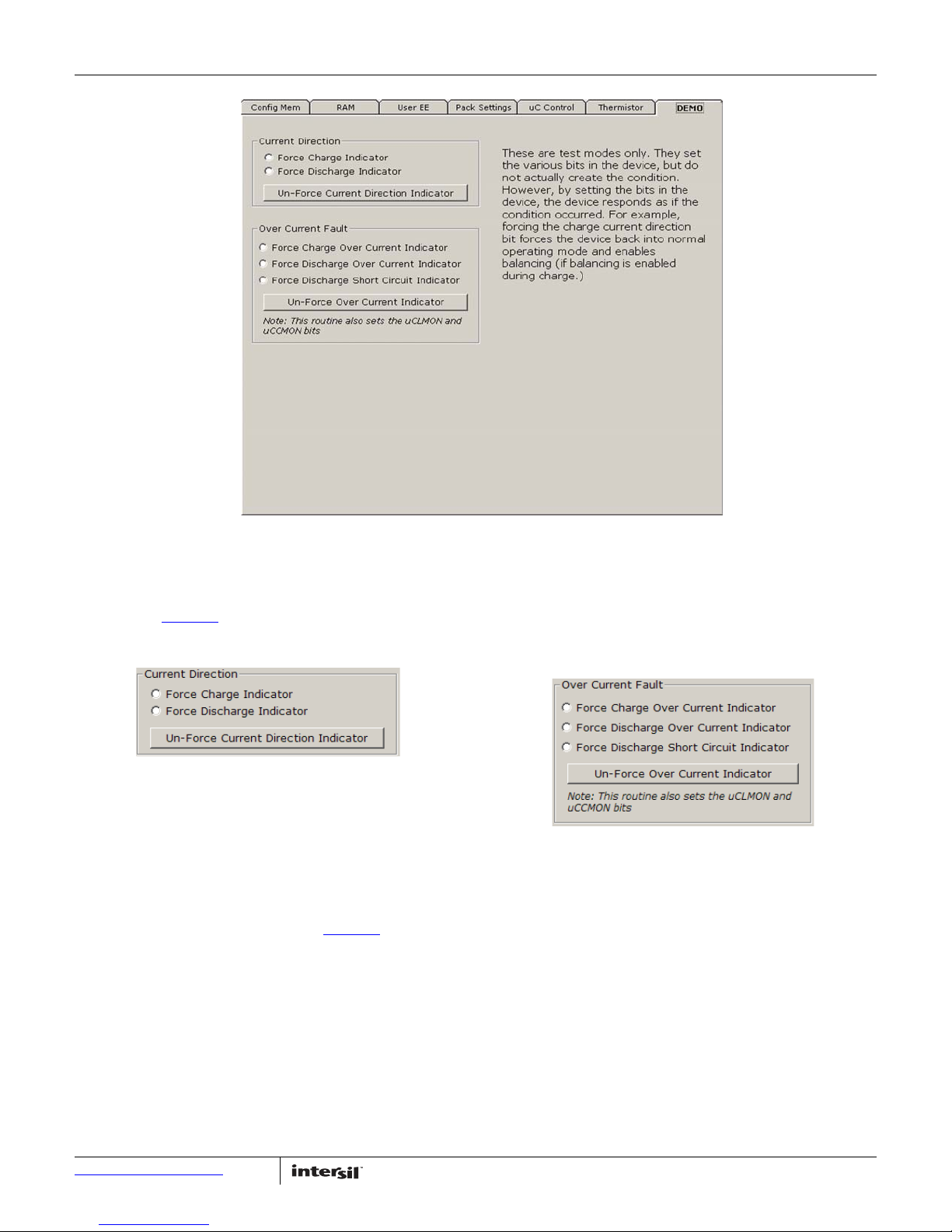
The last tab in the GUI offers some demonstration controls, see
Figure 46. This allows the user to test some items without
connecting a real charger or load to the system. This is useful in
simulating current flow and overcurrent errors.
The controls available in this tab are test modes only. They set
the various bits in the device, but do not actually create the
condition. However, by setting the bits in the device, the device
responds as if the condition occurred. For example, forcing the
charge current direction bit forces the device back into normal
operating mode and enables balancing (if balancing is enabled
during charge).
Submit Document Feedback
24
AN1952.1
July 30, 2015
Page 25
Application Note 1952
FIGURE 46. ISL94203 GUI - DEMO TAB
FIGURE 47.
FIGURE 48. OVERCURRENT FAULT DEMO OPTIONS
CURRENT DIRECTION DEMO
The “Force Charge Indicator” or “Force Discharge Indicator”
controls force the device to indicate a charge or discharge
condition (see Figure 47
). This is not a real condition, for
example, the current readout shows no current flow. However,
the device responds as if there is a current.
While in either of these demo modes, the device will not respond
to real overcurrent or short circuit conditions.
To clear the conditions, click on the “Un-force Current Direction
Indicator” button.
OVERCURRENT DEMO
To simulate any of the overcurrent or short circuit conditions, use
the Over Current Fault demo options (see Figure 48
Charge Over Current Condition” sets the COC bit and the device
responds as if that condition exists. In order to better view the
operation, the GUI sets the µCLMON and µCCMON bits so the
recovery conditions are controlled manually. Without the
µCCMON and µCLMON bits set, the device will do the following:
• The test bit indicates to the device that there is an overcurrent
condition.
• The device sees that there is no current, so starts the LDMON
or CHMON operation.
). The “Force
• The device sees that there is no load and no charger, so it
clears the fault condition.
• The device immediately sees the test mode fault condition, so
it again responds as if there is fault.
• The device continues to “oscillate” between these modes,
because the demo condition is not real.
To get a better understanding of the operation, connect a
potentiometer to the load output. Make sure that the minimum
resistance on the potentiometer is about 1kΩ. This is not so low
that it is damaged when the FETs are on, but is low enough to
detect a load. Now, force a discharge overcurrent condition.
(Look at the SD LED on the PCB, it should be on continuously).
Use the µC Control tab to clear the µC Load Monitor bit. Now, the
device detects the overcurrent (from the test bit). It sees that
there is no current, so it starts the load monitor. Because of the
potentiometer, it sees that there is a load, so the fault condition
remains in effect and the SD LED remains on. By gradually
increasing the resistance on the potentiometer, the device will
reach the point where the device detects that the load is
removed. At this point, the SD LED will resume the “oscillations”
as it detects the load clearing and sees the demo fault.
Submit Document Feedback
25
AN1952.1
July 30, 2015
Page 26
Application Note 1952
26
AN1952.1
July 30, 2015
Submit Document Feedback
ISL94203EVKIT1Z Hardware Design
R40
1k
R41
1k
R42
1k
R43
1k
R44
1k
R45
1k
R46
1k
R47
1k
R48
1k
C3
1uF
R62
22k
R61
22k
R37
100
R35
100
C23
4.7nF
C22
4.7nF
R66
499
R67
499
GND
R34
1k
R59
.002/1W
1
RGO
RGO
R68 4.7k
R69 4.7k
C2 1uF
GND
1
J1
CON1
1
TP9
GND
GND
R39 100
R38 100
R58
.002/1W
J7
xT2 select
Note:
Th2b is physicall
located under t
h
Discharge FET.
xTH2a
Therm2a
xTH1
Therm1
J6
ADDR
S2
FETSOFF
R17
10k
R75 120k
C41uF
S1
WakeUp
R63
1k
R26
100/1W
R18
1k
R9 10k
R1
330k
R27
100/1W
R19
1k
R10
10k
R2
330k
Q8
NDS0605
R28
100/1W
R20
1k
R11
10k
R3
330k
R33
100/1W
R25
1k
R16
10k
R8
330k
Q5
NDS7002A
R32
100/1W
R24
1k
R15
10k
R7
330k
R31
100/1W
R23
1k
R14
10k
R6
330k
R30
100/1W
R22
1k
R13
10k
R5
330k
R29
100/1W
R21
1k
R12
10k
R4
330k
C1 47nF/50V
C13
47nF
CB8
CB7
CB6
CB5
CB4
CB3
CB2
CB1
CB8
CB7
CB6
CB5
CB4
CB3
CB2
CB1
C6
7
C5
6
C4
5
C3
4
C2
3
C1
2
C0
1
C7
8
C8
9
J3
Battery Connect
R36
100
R54
200/1W
C14
47nF
C15
47nF
C16
47nF
C17
47nF
C18
47nF
C19
47nF
C20
47nF
C21
47nF
Q7
NDS0605
Q6
NDS0605
Q4
NDS7002A
Q3
NDS7002A
Q2
NDS7002A
Q1
NDS7002A
ISL94203EVAL1Z
Title
Size
B ISL94203EVAL1Z
Date:
File:
1of 1
Revsion
Drawn by:
Number
Nov 12, 2013
ISL94203EVAL1Z
D
Sheet
CEM
VC8
1
CB8
2
VC7
3
CB7
4
VC6
5
CB6
6
VC5
7
CB5
8
VC4
9
CB4
10
VC3
11
CB3
12
VC213CB214VC115CB116VC017VSS18VREF19xT120xT221TEMPO22NC23ADDR
24
SCL
25
SDAI
26
SDAO
27
GND
28
GND
29
NC
30
INT
31
PSD
32
FETSOFF
33
SD
34
EOC
35
RGO
36
VBATT
48
CS147CS2
46
CFET
45
PCFET
44
VDD
43
DFET
42
C141C240C3
39
LDMON
38
CHMON
37
PAD
0
U1
ISL94203
D25
PSD
R52
1k
R73
49.9k
R64
1M
R65
1M
J9
Path2
Single Path
Split Path
VBATT
VBATT
R56
1M
R55
1M
R57
1M
D20
18V
D18
18V
D19
18V
Th2a XH103F
Th1 XH103F
Th2b XH103F
1
FETSOFF
FETSOFF
VBATT
R60
68m
C24
4.7uF/50V
D21
V10P10
1
2
3
4
J13
I2C
1
J11
DSCG+
1
J10
CHRG+
1
TP10
GND
1
TP11
GND
1
VC8
VC8
1
VC7
VC7
1
VC6
VC6
1
VC5
VC5
1
VC4
VC4
1
VC3
VC3
1
VC2
VC2
1
VC1
VC1
C6
7
C5
6
C4
5
C3
4
C2
3
C1
2
C0
1
C7
8
C8
9
J2
Test points
1
CB8
CB8
1
CB7
CB7
1
CB6
CB6
1
CB5
CB5
1
CB4
CB4
1
CB3
CB3
1
CB2
CB2
1
CB1
CB1
1
CFET
CFET
1
PCFET
PCFET
1
DFET
DFET
1
LDMON
LDMON
1
CHMON
CHMON
1
xT1
xT1
1
xT2
xT2
1
TMPO
TMPO
1
VREF
VREF
1
SDA
SDA
1
SCL
SCL
Note:
Maximum continuous charge current = 2.5A
Maximum continuous discharge current = 20A
Over charge current = 8A/1s
Over discharge current = 30A/500ms
Short circuit current = 75A/200us
D26
RGO
R53
1k
R74 49.9k
Q16
MBT3904DW1
Q15
MBT3904DW1
D23
SD
R71 49.9k
R50
1k
Q13
MBT3904DW1
D22
EOC
R70 49.9k
R49
1k
Q12
MBT3904DW1
C28
2.2uF
R76
0
R78
2.49k
R79
2.49k
R81
2.49k
R82
2.49k
1
2
3
4
5
6
7
8
J5
STAT/CNTRL
YLOW
YLOW
YLOW
YLOW
YLOW
YLOW
YLOW
YLOW
RED RED
RED
GRN
D1
LED
D2
LED
D3
LED
D4
LED
D5
LED
D6
LED
D7
LED
D8
LED
1
23
Q9
IRF1010
1
2 3
Q10
IRF1010
1
23
Q11
BSS170
1
VB
VB
1
VC0
VC0
1
TP1
GND
1
CS1
CS1
1
CS2
CS2
Intersil
Logo
INTERSIL LOGO
Pb
ROHS
ROHS
ROHS
R83
3.3M
R84
549k
GND
IO1
1
GND
2
IO23IO2
4
VBUS
5
IO1
6
U2
USBLC6-2SC6
C27
1nF
C25
1uF
C26
1uF
1
32
D29
MMBD7000
R86 10k
R85 10k
D30
3.3V
SMAJ40CA
SMAJ40CA
D27
TVS BIDIR
D28
TVS BIDIR
D34
TVS BIDIR
D32
43V
SMAJ40CA
D3343V
D31
43V
Notes:
- Add a 3.3M resistor (or higher) from
LDMON to GND and CHG+ to DSCG+
to allow sleep mode in 2Path configura
t
- Add a 2.2nF cap from SD, EOC to GND.
(Prevent spike when the pin goes high.)
- Add 1 schottky diode to VDD to get bet
t
accuracy in single power path conection.
- Zener diodes on cell balance circuits
removed. (They were not needed.)
- Add FETs to I2C inputs to prevent
powering ISL94203 through the uC.
- Remove cell to cell caps and increase c
e
to gnd caps.
- Replace power FETs to increase max
voltage.
- Added resistors in current sense circuit
f
test purposes.
- Change resistor values for R83, R84 to
reduce current.
R87
3.3M
ADD for better sleep in 2 path connection
C31
2.2nF
C32
2.2nF
ADD to reduce switching spikes
D37
PMEG6002
ADD for lower drop in VDD
Improves accuracy
ADD to prevent
powering IC from I2C
RGO
J4
Path1
Single Path
Split Path
1 6
423
5
U3
SI1970
when Q9 is off
R51
3.3M
60V/75A
60V/75A
60V/500mA
D36
PMEG6002
R72
100
R77
100
Added
resistors t
o
test effect
on current
sense
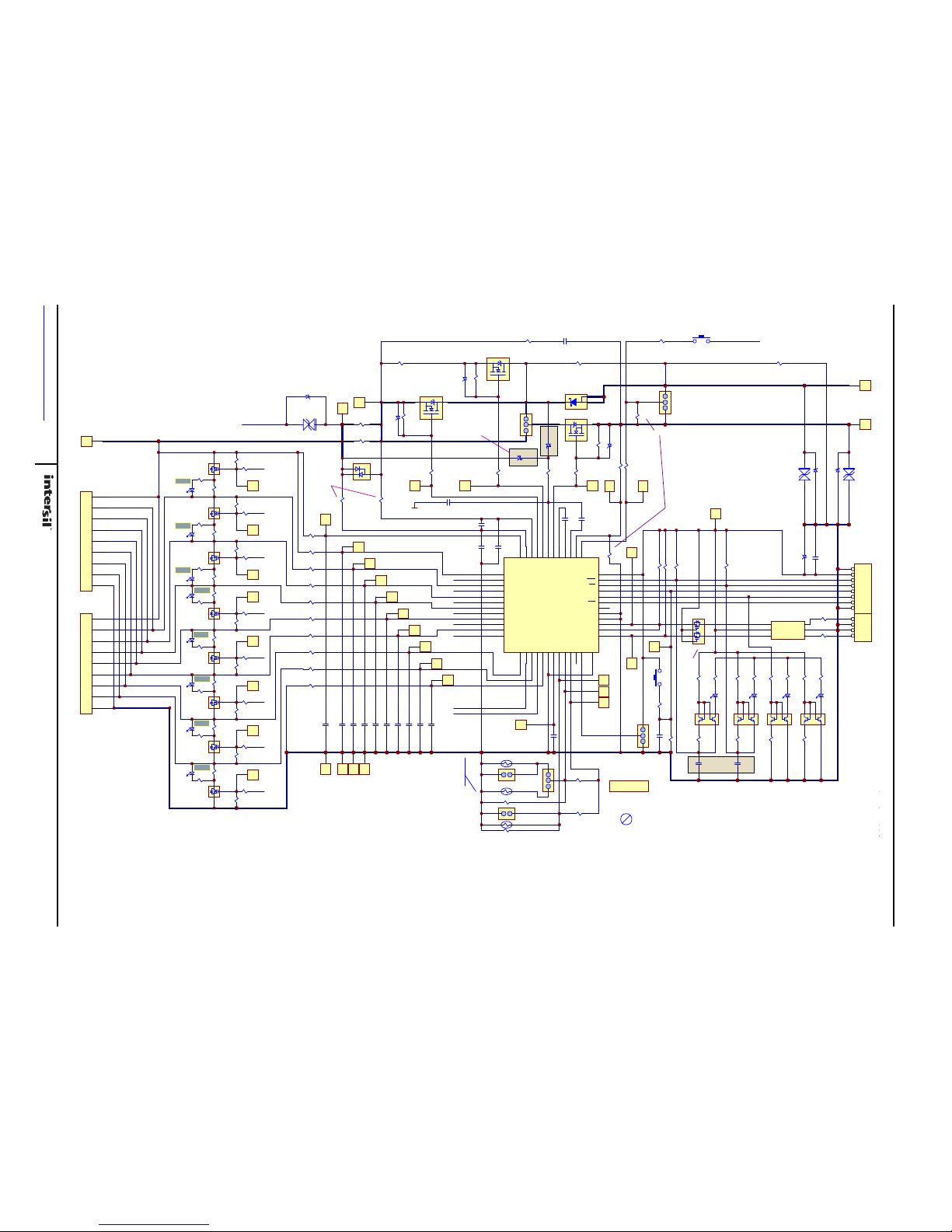
FIGURE 49. ISL94203EVKIT1Z HARDWARE DESIGN
Page 27
Application Note 1952
Bill of Materials
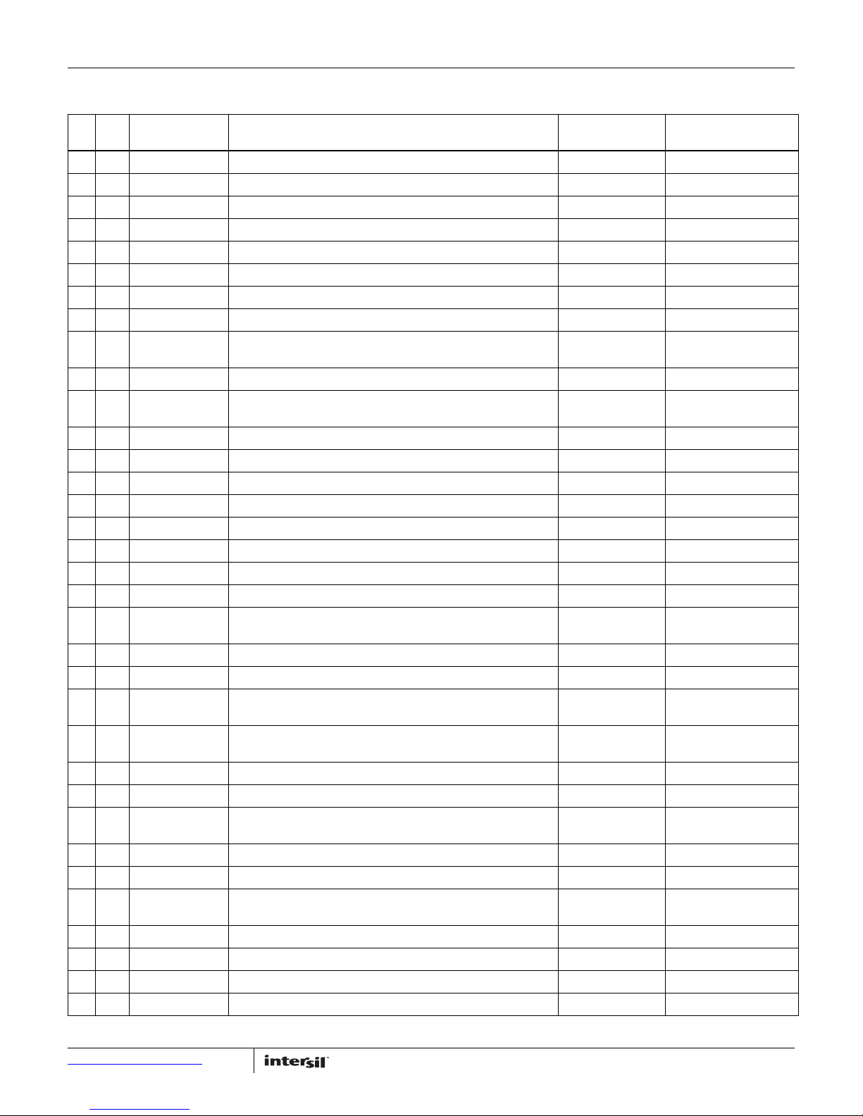
REFERENCE
QTY UNIT
10 ea. C1, C13-C21 CAP, SMD, 0603, 47nF, 100V, 10%, X7R, ROHS VENKEL C0603X7R101-473KNE
3 ea. C2, C25, C26 CAP, SMD, 0603, 1µF, 50V, 10%, X5R, ROHS TDK C1608X5R1H105K
2 ea. C22, C23 CAP, SMD, 0603, 4700pF, 100V, 10%, X7R, ROHS VENKEL C0603X7R101-472KNE
1 ea. C27 CAP, SMD, 0603, 1000pF, 16V, 10%, X7R, ROHS VENKEL C0603X7R160102KNE
1 ea. C28 CAP, SMD, 0603, 2.2µF, 10V, 10%, X7R, ROHS MURATA GRM188R71A225KE15D
2 ea. C3, C4 CAP, SMD, 0603, 1.0µF, 10V, 10%, X7R, ROHS AVX 0603ZC105KAT2A
2 ea. C31, C32 CAP, SMD, 0603, 2.2nF, 100V, 10%, X7R, ROHS VENKEL C0603X7R101-222KNE
3 ea. D18-D20 DIODE-ZENER, SMD, 2P, SOD-123, 18V, 500mW, ROHS DIODES INC. MMSZ5248B-7-F-T
8 ea. D1-D8 LED-SMART, SMD, 0603, YELLOW, 1.8V, 2mA, 587nm, 7.9mcd,
1 ea. D21 DIODE-RECTIFIER, SMD, SMPC, 100V, 10A, ROHS VISHAY V10P10-M3/86A
3 ea. D22-D23, D25 LED-SMART, SMD, 0603, 2P, RED, 1.8V, 2mA, 630nm, 4.5mcd,
1 ea. D26 LED-SMART, SMD, 0603, GREEN, 1.7V, 2mA, 570nm, 3.9mcd, ROHS OSRAM LGL29K-G2J1-24-Z
3 ea. D27, D28, D34 DIODE-TVS, BIDIRECTIONAL, SMD, 2P, SMA, 40V, 400W, ROHS DIODES, INC. SMAJ40CA-13-F
1 ea. D29 DIODE-DUAL, SWT, SMD, SOT23, 100V, 2A, 350mW, ROHS DIODES INC. MMBD7000HS-7-F
1 ea. D30 DIODE-ZENER, SMD, 2P, SOD-123, 3.3V, 500mW, ROHS DIODES, INC. BZT52C3V3-7-F
3 ea. D31, D33, D32 DIODE-ZENER, SMD, SOD-123, 43V, 410mW, ROHS DIODES, INC. BZT52C43-7-F
1 ea. D35 Diode Schottky, SOD323
2 ea. D36, D37 Diode, Schottky, SOD523
1 ea. Q11 TRANSIST-MOS, N-CHANNEL, SMD, DPAK, 40V, 9A, ROHS FAIRCHILD FDD8451
4 ea. Q12, Q13, Q15,
5 ea. Q1-Q5 TRANSISTOR-MOS, N-CHANNEL, SMD, SOT23, 60V, 280mA, ROHS FAIRCHILD NDS7002A
3 ea. Q6-Q8 TRANSISTOR, P-CHANNEL, SMD, SOT23, -60V, -180mA, ROHS FAIRCHILD NDS0605
2 ea. Q9, Q10 TRANSISTOR-MOS, N-CHANNEL, SMD, D2PAK, 40V, 75A, ROHS NXP
12 ea. R18-R25, R49,
8 ea. R1-R8 RES, SMD, 0603, 330k, 1/10W, 1%, TF, ROHS YAGEO RC0603FR-07330KL
8 ea. R26 - R33 RES, SMD, 2512, 100Ω, 1W, 1%, TF, ROHS VISHAY/DALE CRCW2512100RFKEG
11 ea. R34, R40-R48,
6 ea. R35-R39 RES, SMD, 0603, 100Ω, 1/10W, 1%, TF, ROHS VENKEL CR0603-10W-1000FT
1 ea. R54 RES, SMD, 2512, 200, 1W, 5%, TF, ROHS VENKEL CR2512-1W-201JT
5 ea. R55-R57, R64,
2 ea. R58, R59 RES, SMD, 2512, 002Ω, 1W, 1%, TF, ROHS PANASONIC ERJ-M1WTF2M0U
2 ea. R61, R62 RES, SMD, 0402, 22k, 1/16W, 1%, TF, ROHS VENKEL CR0402-16W-223JT
2 ea. R66, R67 RES, SMD, 0603, 499Ω, 1/10W, 1%, TF, ROHS VENKEL CR0603-10W-4990FT
2 ea. R68, R69 RES, SMD, 0402, 4.7k, 1/16W,1%,TF,ROHS VENKEL CR0402-16W-4701FT
DESIGNATOR DESCRIPTION MANUFACTURER MANUFACTURER PART
OSRAM LY L29K-J1K2-26-Z
ROHS
OSRAM LSL29K-G1J2-1-0-2-R18-Z
ROHS
TRANSISTOR-DUAL NPN, SMD, 6P, SOT363, 40V, 200mA, ROHS DIODES, INC. MMDT3904-7-F
Q16
PHB101NQ04T
SEMICONDUCTOR
RES, SMD, 0402, 1k, 1/16W, 1%, TF, ROHS VENKEL CR0402-16W-102JT
R50, R52, R53
RES, SMD, 0603, 1k, 1/10W, 1%, TF, ROHS PANASONIC ERJ-3EKF1001V
R63
RES, SMD, 0603, 1M, 1/10W, 1%, TF, ROHS PANASONIC ERJ-3EKF1004V
R65
Submit Document Feedback
27
AN1952.1
July 30, 2015
Page 28
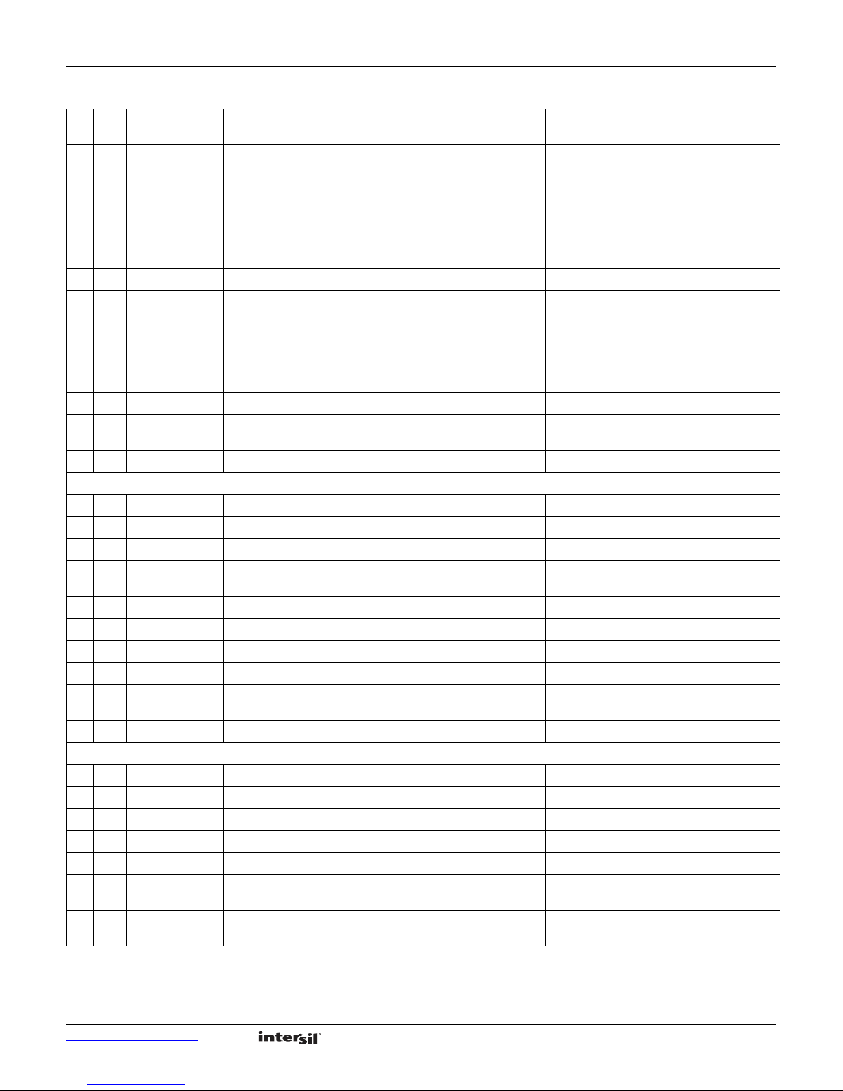
Bill of Materials (Continued)
Application Note 1952
QTY UNIT
5 ea. R70-R74 RES, SMD, 0402, 49.9k, 1/16W, 1%, TF, ROHS PANASONIC ERJ-2RKF4992
1 ea. R75 RES, SMD, 0603, 120k, 1/10W, 1%, TF, ROHS VISHAY/DALE CRCW0603120KFKEA
1 ea. R76 RES, SMD, 0603, 0Ω, 1/10W, TF, ROHS VENKEL CR0603-10W-000T
1 ea. R77 RES, SMD, 0402, 0Ω, 1/16W, 5%, TF, ROHS VENKEL CR0402-16W-00T
4 ea. R78, R79, R81,
2 ea. R83, R87 RES, SMD, 0603, 3.3M, 1/10W, 1%, TF, ROHS PANASONIC ERJ-3EKF3304V
1 ea. R84 RES, SMD, 0603, 550k, 1/10W, 1%, TF, ROHS VENKEL CR0603-10W-5503FT
11 ea. R9-R17, R85, R86 RES, SMD, 0402, 10k, 1/16W, 1%, TF, ROHS PANASONIC ERJ-2RKF1002X
2 ea. S1, S2 SWITCH-TACTILE, PUSH, TH, 8X8mm, SPST, 12V, 50mA, ROHS OMRON B3WN-6002
3 ea. Th1, TH2a, TH2b THERMISTOR, SMD, 0603, 10k, 1/10W, 5%,
1 ea. U1 IC-MULTI-CELL, LI-ION MONITOR, 48P, QFN, 6X6, ROHS INTERSIL ISL94203IRTZ
1 ea. U2 IC-TVS, ESD PROTECTOR, SMD, 6P, SOT-23-6L, 3pF, 6V, ROHS ST
1 ea. PWB-PCB, ISL94203EVKIT1Z, REVD, ROHS
CONNECTORS/HEADERS
1 ea. J13 CONN-HEADER, 4PIN, 2.54mm, RIGHT-ANGLE, ROHS MOLEX 22-05-2041
1 ea. J3 CONN-HEADER, 1X9, FLAT BRK-AWAY, 2.54mm, R/A, ROHS MOLEX 22-28-8091
1 ea. TP11 CONN-HEADER, 1x1, BREAKAWAY 1X36, 2.54mm, ROHS BERG/FCI 68000-236HLF
4 ea. 1Path, 2Path,
3 ea. ADDR, J7, J9 CONN-HEADER, 1x3, BREAKAWY 1X36, 2.54mm, ROHS BERG/FCI 68000-236HLF
1 ea. J5 CONN-HEADER, 1X8, BRKAWY 1X36, 2.54mm, ROHS BERG/FCI 68000-236HLF
1 ea. J2 CONN-HDR, 1x9, BRKAWY 1X36, 2.54mm, ST, ROHS BERG/FCI 68000-236
1 ea. CS1, CS2 CONN-HEADER, 1X2, BRKAWY 1X64, 2.54mm, 0.195x0.118, ROHS MILL-MAX 800-10-064-10-001000
1 ea. CHMON, LDMON,
1 ea. VB, VC0-VC8 CONN-HDR, 1X10, BRKAWY 1X64, 2.54mm, 0.195x0.118. ROHS MILL-MAX 800-10-064-10-001000
DO NOT POPULATE
0 ea. C24 CAP, SMD, 1206, ROHS
0 ea. R60 RES, SMD, 0805, 68mΩ, ROHS
0 ea. J1, J10, J11 DO NOT POPULATE
0 ea. TP1, TP9, TP10 DO NOT POPULATE
0 ea. CB1-CB8 CONN-HEADER, 1X1, BRKAWY 1X64,2.54mm,0.195x0.118, ROHS MILL-MAX 800-10-064-10-001000
0 ea. SCL, SDA, TMPO,
0ea.FETSOFF, PSD, INT,
REFERENCE
DESIGNATOR DESCRIPTION MANUFACTURER MANUFACTURER PART
RES, SMD, 0402, 2.49k, 1/16W, 1%, TF, ROHS PANASONIC ERJ-2RKF2491V
R82
PANASONIC ERT-J1VG103JA
B VALUE = 3375-3345K, ROHS
USBLC6-2SC6
MICROELECTRONICS
CONN-HEADER, 1x2, BRKAWY 1X36, 2.54mm, ROHS BERG/FCI 68000-236HLF
xTH1, xTH2a
CONN-HEADER, 1X5, BRKAWY 1X64, 2.54mm, 0.195x0.118, ROHS MILL-MAX 800-10-064-10-001000
PCFET, CFET, DFET
CONN-HEADER, 1X3, BRKAWY 1X64, 2.54mm, 0.195x0.118, ROHS MILL-MAX 800-10-064-10-001000
VREF, xT1, xT2
CONN-HEADER, 1X6, BRKAWY 1X64, 2.54mm, 0.195x0.118, ROHS MILL-MAX 800-10-064-10-001000
SD, EOC, RGO
Submit Document Feedback
28
AN1952.1
July 30, 2015
Page 29
Layout
Application Note 1952
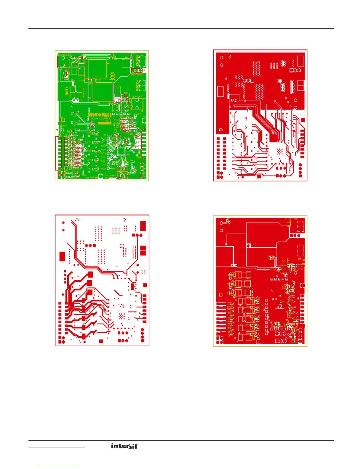
FIGURE 50. TOP LAYER FIGURE 51. MIDDLE LAYER 1
FIGURE 52. MIDDLE LAYER 2
Hardware Overview
The hardware design follows recommendations in the datasheet.
However, this section provides some additional guidelines and
explanations.
Jumpers
There are three user selectable options on the ISL94203EVKIT1Z
board.
Submit Document Feedback
29
FIGURE 53. BOTTOM LAYER
ADDR
This jumper selects the I2C address. Normally this jumper
connects to the “0” position. With the jumper set to the “1”
position, the GUI I
2
C address value must be changed to “52.”
XT2 SELECT
There are three external thermistors on the board. There are two
near the battery connectors. These can be used to monitor the
battery cells (connect external thermistors to connectors xTh1 or
AN1952.1
July 30, 2015
Page 30
Application Note 1952
1 Path
2 Path
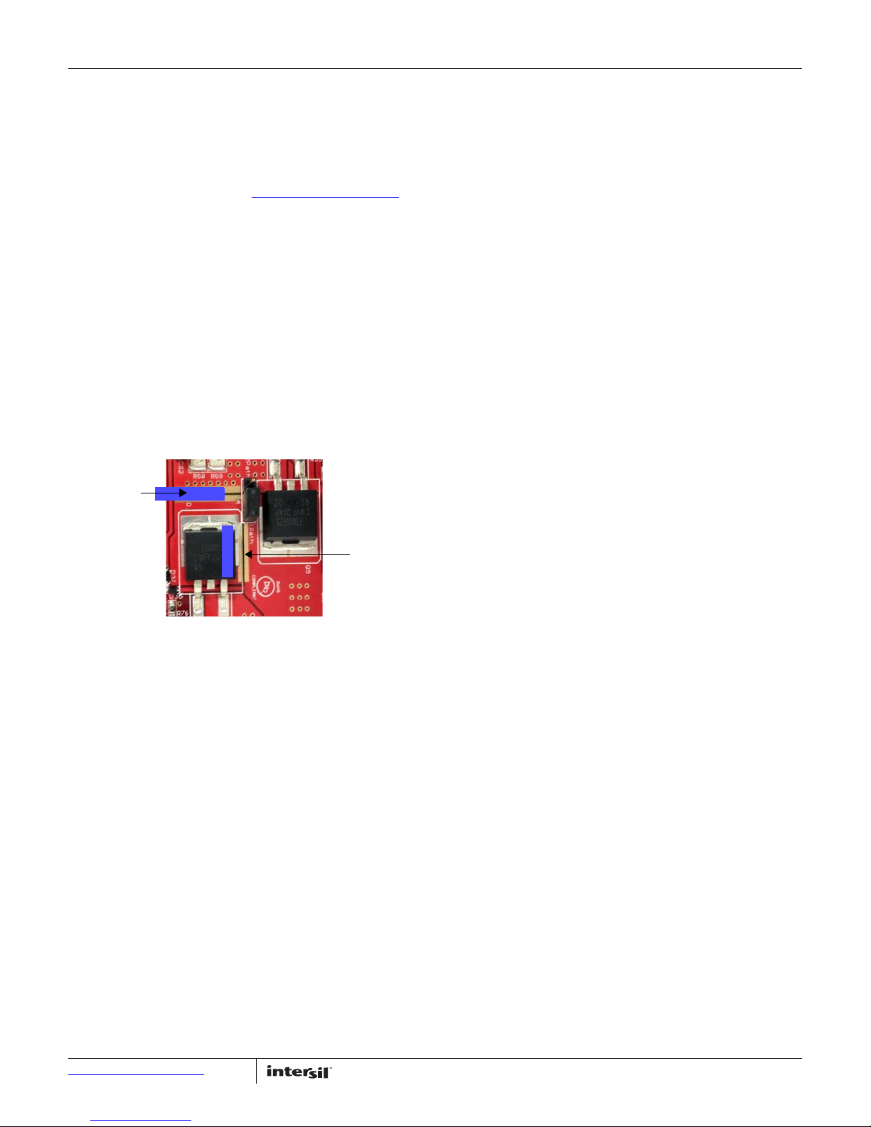
FIGURE 54. SOLDER JUMPERS FOR HIGHER CURRENT
xTH2a and remove the on-board thermistors Th1 and Th2a).
There is a third resistor located under the discharge power FET.
The xT2Select jumper allows the ISL94203 to monitor either the
Th2a thermistor near the battery terminals (CELL position) or the
Th2b thermistor under the power FET (FET position). When
monitoring the FET thermistor, you might want to check the “xT2
Monitors FET” box in the GUI (see “
Pack Options” on page 22).
POWER FET CONFIGURATION
The board allows for both a single charge/discharge path and a
separate charge/discharge path. Configuring the options
requires two jumpers. For a single path, connect a shunt on the
“1Path” aide of J4. Also connect a shunt on the “1Path” side of
jumper J9. In this configuration both charge and discharge
connections of the pack connect to the DSCG+ pin.
For the separate charge and discharge path, connect a shunt on
J4 and J9 on the “2Path” side of each. In this configuration,
discharge is on the DSCG+ pin and charge is on the CHRG+ pin.
If the plan is to test the board with significant amounts of
current, then replace the shunt with some soldered braided wire
to complete the circuit. In this way the board should be able to
handle a discharge current of 20A and charge current of 2.5A.
AFE
The analog front end of the ISL94203 adds external cell
balancing components. The cell balance output from each cell
balance pin is a constant current of about 25µA. This generates
about 8.25V across the 330k resistor between the gate and
source of the balancing transistor. If a balance FET with lower
gate voltage requirements is desired, reduce the value of the
gate resistor.
The evaluation board uses 100Ω cell balance resistors, so it
balances about 40mA of current. The board also includes LEDs
on each cell balance circuit to indicate when the cell balance is
active.
The cell input filters consist of a 1k resistor, a 4.7nF capacitor to
ground, and a 10nF capacitor cell-to-cell. These can be changed
to suit the application, but the following guidelines should be
considered.
• The 1k resistor can be reduced, but this makes the part more
susceptible to input currents during hot plug of the battery
cells. A smaller input resistor would also require higher value
capacitors to ground to maintain the same filter. Higher value
resistors on the upper cells would be higher cost.
• The 1k resistor can be increased. The limit relates to the
accuracy of measurement. In the worst case conditions, there
is a difference of about 2µA of bias current on the inputs. The
ISL94203 is factory calibrated assuming an input 1k resistor.
An extra 1k input resistor can generate up to 2mV of error.
Larger input resistors increase this error.
• The capacitors from each input to ground provide a better filter
than the capacitors across each input. However, differences in
capacitors on adjacent inputs could result in some voltage
errors on the input. Both capacitors to ground and capacitors
across inputs are provided on the board, but the application
may not need both.
• Larger input capacitors can affect the open wire detection
circuit. If larger capacitors are used and the open wire circuit
does not seem to detect the open condition, increase the
“Open Wire Sample Time” timer value in the GUI.
Protection Circuits
The board contains several protection components that should
be on any application.
• There should be diodes on VBATT, DSCG+, and CHRG+ to GND
to prevent negative voltages on the pins of the ISL94203. The
schematics show the use of 43V zener diodes, so the inputs
are also protected against high voltage transients.
• The board provides transient voltage suppressors on the pack
pins to help minimize problems with ESD on the board.
2
• There is a protection device (USBLC6) on the I
minimize damage due to ESD on the I2C connector. While this
component helps protect against ESD, it is also a problem for
the board. Since this component has internal diodes between
the I2C pins and the RGO power pin, connecting the I
interface to an externally powered µC before the ISL94203
powers up prevents proper power-up of the ISL94203. If there
is a hardwired connection between the µC and the evaluation
board, U2 can be removed from the board and replaced with
jumpers across pins 1 to 6 and 3 to 4. This will allow the µC to
power up before the ISL94203 powers up.
• Back to back diodes are connected across the current sense
inputs to prevent excessive differential voltage across these
pins.
C inputs to
2
C
Push Buttons
The board provides two push buttons for ease of use and
evaluation purposes. These are not required in an application.
• The wake up push button simulates the connection of a pack
to a charger. It does this by connecting the CHRG+ pin to VDD
using a 1k series resistor. The device sees this as a charger
connection. The ISL94203 can also be wakened by
momentarily connecting a resistor from the DSCG+ pin to
GND. Use a 2k resistor to minimize current when the power
FETs turn on. During manufacture of the battery pack, the
finished pack can be connected to a charger, or this wake up
switch can be included on an external jig to power up the board
prior to final programming.
• The FETSOFF pin connects directly to the FETSOFF input of the
ISL94203. When pressed, the power FETs and cell balance
Submit Document Feedback
30
AN1952.1
July 30, 2015
Page 31
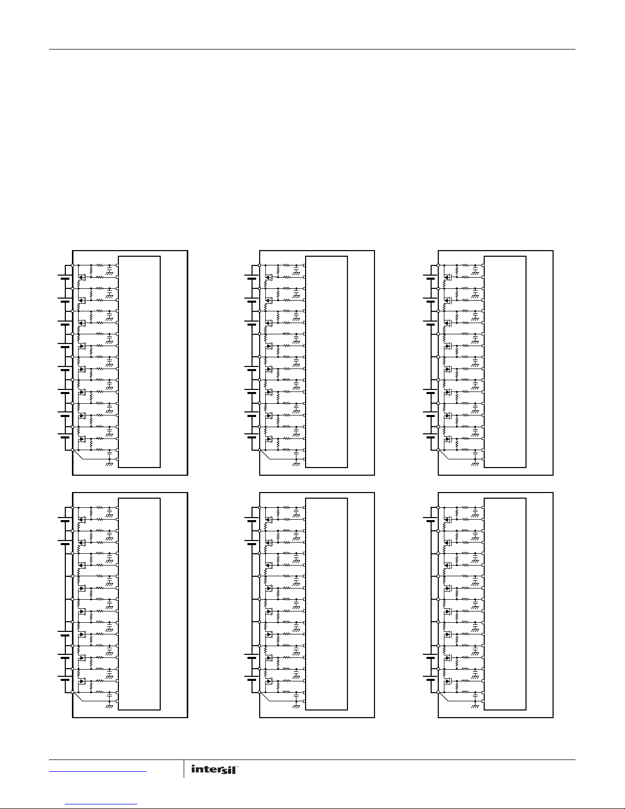
Application Note 1952
6 CELLS
3 CELLS4 CELLS
VCELL7
VCELL6
VCELL5
VCELL4
VCELL3
VCELL2
VCELL1
VSS
8 CELLS
CB7
CB6
CB5
CB4
CB3
CB2
CB1
FIGURE 55. BATTERY CONNECTION OPTIONS USING THE ISL94203EVKIT1Z BOARD
VCELL8
CB8
VCELL0
5 CELLS
7 CELLS
VCELL7
VCELL6
VCELL5
VCELL4
VCELL3
VCELL2
VCELL1
VSS
CB7
CB6
CB5
CB4
CB3
CB2
CB1
VCELL8
CB8
VCELL0
VCELL7
VCELL6
VCELL5
VCELL4
VCELL3
VCELL2
VCELL1
VSS
CB7
CB6
CB5
CB4
CB3
CB2
CB1
VCELL8
CB8
VCELL0
VCELL7
VCELL6
VCELL5
VCELL4
VCELL3
VCELL2
VCELL1
VSS
CB7
CB6
CB5
CB4
CB3
CB2
CB1
VCELL8
CB8
VCELL0
VCELL7
VCELL6
VCELL5
VCELL4
VCELL3
VCELL2
VCELL1
VSS
CB7
CB6
CB5
CB4
CB3
CB2
CB1
VCELL8
CB8
VCELL0
VCELL7
VCELL6
VCELL5
VCELL4
VCELL3
VCELL2
VCELL1
VSS
CB7
CB6
CB5
CB4
CB3
CB2
CB1
VCELL8
CB8
VCELL0
FETs turn off. Normally in a system, this input would connect to
a µC or an external control source. If FETSOFF connects off
board, add a 3V zener diode to GND to prevent glitches on this
input from going too high or negative.
LED Indicators
There are 4 LED indicators on the board. The LEDs are not
required in a real application, they are used here to provide quick
monitoring of the system. The LEDs are RGO (Green), EOC (Red),
SD (Red), and PSD (Red).
The LED indicator circuits use current mirrors to drive the LEDs.
There are several reasons for this.
• The ISL94203 RGO regulator output voltage is 2.5V (2.25V to
2.75V). Because of this voltage and range, it is difficult to
directly drive LEDs that have a forward voltage drop of 1.8V to
2.3V while controlling current to acceptable levels.
• When directly driving the LEDs from the RGO output using a
current limiting resistor, small variations in the supply voltage
result in large changes in LED brightness.
• If the LEDs connect direct to the RGO output, the 4 LEDs would
pull at least 5mA from the RGO output. While this is within the
capability of the RGO, it could lead to some internal heating of
the die. Since this board is for evaluation, and an actual
application would not normally have the LEDs, an indirect
approach to powering the LEDs was adopted.
The current mirrors use a resistor on one side to provide a
“current gain.” The LEDs are each driven with ~ 1mA of current
from VBATT, but the drain from the RGO output is only ~ 40µA.
Submit Document Feedback
31
AN1952.1
July 30, 2015
Page 32

Application Note 1952
Errata/Q&A
1. When I power the board, the device does not power up
correctly. It looks like it is in sleep mode.
Before applying power to the evaluation board, disconnect
the I2C cable. Once the board is powered, then connect the
2
C interface. The reason for this is that U2 on the board has
I
internal protection diodes from the I2C traces to RGO. When
SCL and SDA pull up externally to 3.3V the ISL94203 is
partially powered, so it does not complete its power-up cycle.
2. Cell measurement accuracy does not match the
specifications in the datasheet.
There are some other potential reasons for inaccurate
readings.
• The source of measurement should have a low output
impedance. A string of resistors that sets the input
voltages, like the Intersil MCB_PS_Z board can have small
changes in the input voltage as the ISL94203 samples
each cell. Later models of the MCB_PS_Z board will have
10µF capacitors across each input. These capacitors
should minimize sampling errors.
• The ADC reading should be compared with the voltage on
the PCB before the input resistors (at J2). If the voltages
are compared with DVM readings at the battery pack
where there is a long cable, then there should be separate
wires for GND and VC0; and for VC8 and VBAT. The reason
for this is that the VBAT and GND leads will carry perhaps a
lot of current, so there may be voltage drops across the
wires. The VC0 and VC8 terminals are “Kelvin” connections
that do not carry much current. Cell voltage
measurements are based on VC0 and VC8, not GND and
VBAT.
• Soldering the board to the PCB can change the stresses on
the package from what they were during device
calibration. This can change the value of the voltage
reference, which changes the ADC converted value. This
does not affect the relative voltage readings. If there is an
external µC, then an offset can be added to the µC to
correct for solder induced stresses.
3. I changed the “Pack Settings” tab such that the “CB during
EOC” button is checked. But after power cycling the part, the
“CB during EOC” is no longer checked and the part is not
balancing during End of Charge.
• After clicking on any of the option bits in the “Pack
Settings” tab or on the main screen (above the FET control
indicators) it is necessary to do a “Write EEPROM” either
on the “Pack Settings” tab or the “Config Mem” tab.
Without this write operation the change only resides in the
ISL94203 Configuration RAM space.
4. When I repeatedly read the EEPROM memory in the
configuration tab, the communications lock up.
• There was a problem with the old GUI code. The best
solution is to get the new Win7/8 code. This new code
does not have this problem. Until then, the best way to
clear this, without removing the battery from the board, is
to remove the I
connect and release the SCL line to VSS (it is pulled up by
a resistor). This creates a clock pule. Do this up to 9 times
to clear the ISL94203 port. Then reconnect the I
2
C cable and use a jumper to momentarily
2
C cable.
Submit Document Feedback
32
AN1952.1
July 30, 2015
Page 33
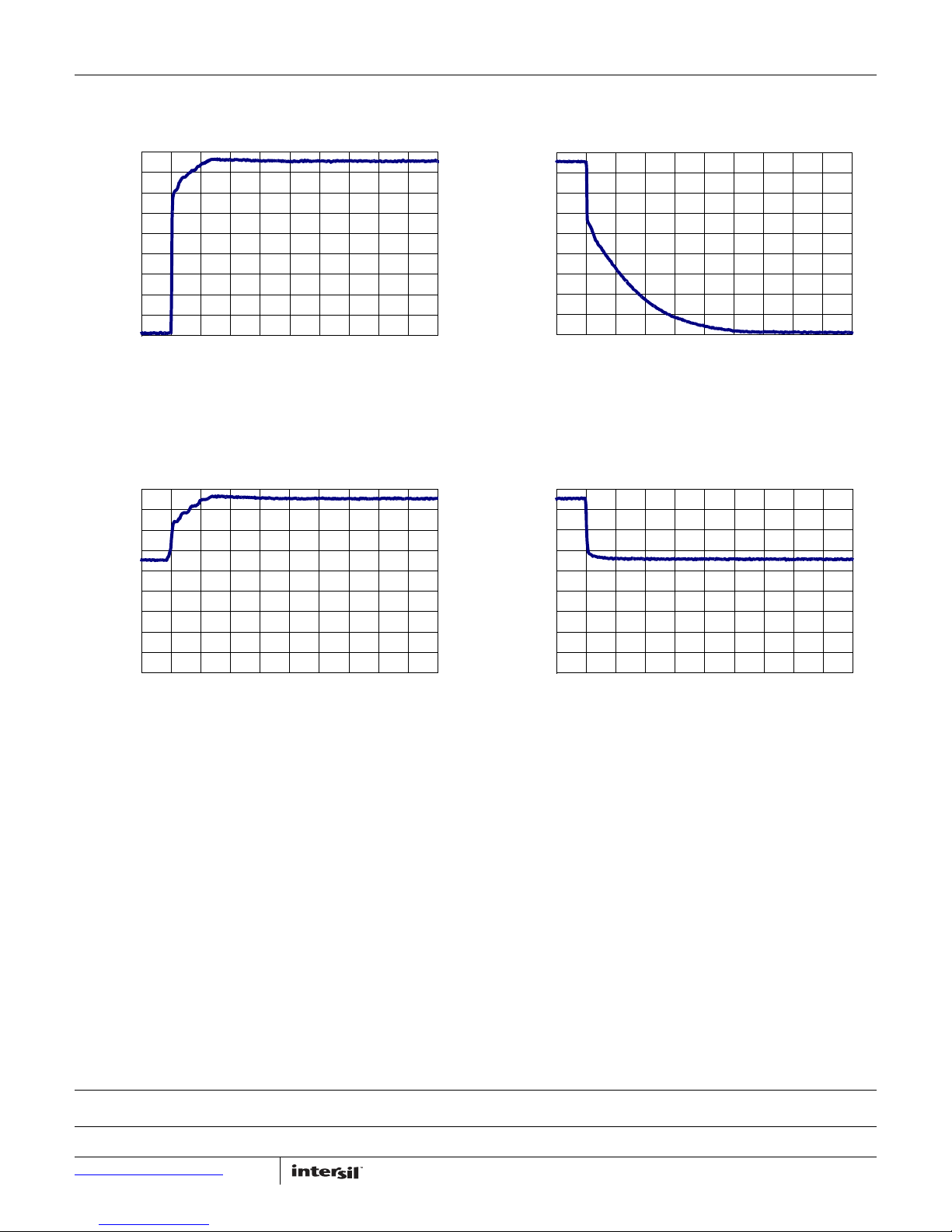
Application Note 1952
0
5
10
15
20
25
30
35
40
45
AMPLITUDE (V)
TIME (100µs/DIV)
0
5
10
15
20
25
30
35
40
45
TIME (1ms/DIV)
AMPLITUDE (V)
5
10
15
20
25
30
35
40
45
TIME (100µs/DIV)
AMPLITUDE (V)
0
0
5
10
15
20
25
30
35
40
45
TIME (100µs/DIV)
AMPLITUDE (V)
FET Gate Drive Rise/Fall Characteristics Verify basic digital logic, analog interface, level shifters and
charge pump operation.
FIGURE 56. DFET RISE FIGURE 57. DFET FALL
FIGURE 58. CFET RISE
Intersil Corporation reserves the right to make changes in circuit design, software and/or specifications at any time without notice. Accordingly, the reader is
Submit Document Feedback
For information regarding Intersil Corporation and its products, see www.intersil.com
33
cautioned to verify that the document is current before proceeding.
FIGURE 59. CFET FALL
AN1952.1
July 30, 2015
 Loading...