

Page 1
Application Note 1589
ISL9220IRTZEVAL1Z (1-cell), ISL9220AIRTZEVAL1Z
(2-cell) Evaluation Board
Evaluation Board Features
• Operating Input Voltage Range:
- 4.5V to 14V for ISL9220IRTZEVAL1Z
- 9.0V to 14V for ISL9220AIRTZEVAL1Z
• Up to 2A Charge Current
•Two Status Outputs
• 1.2MHz Switching Frequency
• Connector, Test Point and Jumper
Required Equipment
• Power Supply (PS1 & PS2) Capable of Supplying up to 18V
and 3A
• Electronic Load (E-Load) (20V/5A), Voltmeter, Oscilloscope
February 9, 2012
AN1589.2
1
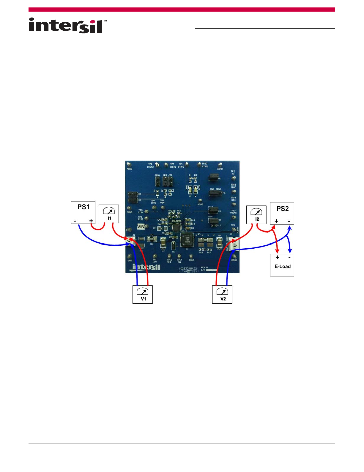
FIGURE 1. QUICK SETUP DIAGRAM
CAUTION: These devices are sensitive to electrostatic discharge; follow proper IC Handling Procedures.
1-888-INTERSIL or 1-888-468-3774
Intersil (and design) is a trademark owned by Intersil Corporation or one of its subsidiaries.
|Copyright Intersil Americas Inc. 2011, 2012. All Rights Reserved
All other trademarks mentioned are the property of their respective owners.
Page 2
Application Note 1589
Quick Setup Guide
1. Insert shunts on left two pins of H6, H5 for normal operation
and H4 to disable timeout if needed.
2. Connect power supply (PS1) in series with a current meter (I1)
to connector IN+.
3. Connect power supply (PS2) in series with a current meter (I2)
to VBAT pin of J2.
4. Connect electronic load (E-load) setting at 2.2A to VBAT pin
and ground.
5. Connect a voltage meter (V2) on TP6 to measure voltage on
VBAT.
6. Place a scope probe on the connector of TP14 to monitor
switching waveform.
7. Set input supply PS1 voltage between 4.5V to 14V for 1-cell
charge and 9V to 14V for 2-cell charge.
8. Set PS2 so that V2 measures 3.6V on VBAT for 1-cell and 7V
for 2-cell.
9. Turn on PS1. LED2 will turn on red indicating power good.
10. Turn on PS2 and E-load. LED1 will turn on green indicating
charging in progress.
11. Without shunts on JP8 and JP9, current meter I2 will measure
500mA ±10% charge current.
12. Insert a shunt on JP8. The resistance on the ISET1 pin
becomes 33.3kΩ and I2 will measure 1.5A±10% charge
current.
13. Insert shunt on JP9. The resistance on the ISET1 pin becomes
25kΩ and I1 will measure 2A±10% charge current.
14. Lower the voltage on PS2 until V2 measures 2.5V for 1-cell
and 5V for 2-cell. The charger will become trickle mode. I2 will
measure around 70mA trickle charge current.
15. Insert a shun t on J P10. I 2 will m easure aro und 140 mA tric kle
charge current. For Steps 11 to 15, you should see 1.2MHz
switching waveform on the scope.
16. Lower the voltage on PS2 until V2 measures less than 2.5V for
1-cell and less than 5V for 2-cell. The charger will charge in
LDO mode current. I2 will measure around 50mA LDO
current. The charge stops switching in this mode.
17. Slowly increase the voltage on PS2; the charge current into the
PS2 reduces. As current continues to reduce and reaches
around 100mA, the end-of-charge event happens and the
charger stops charging. At this point, V2 should measure 4.2V,
±1% for 1-cell and 8.4V, ±1% for 2-cell. STAT1 toggles high, and
LED2 turns off. Remove the shunt from JP10, the end-of-charge
current changes to 50mA.
18. Charging efficiency can be calculated by
(V
)/(VIN*IIN)*100. The voltage and current can be read
O*IO
from V1, I1, V2 and I2.
R1
C1
OPEN
1210
ISET1
R6
50kΩ
JP8
ISET2
TP13
0.03Ω
1210
R7
1000kΩ
JP9
R9
600kΩ
JP10
R2
22
C4
10nF/50V
R8
100kΩ
R10
600kΩ
C2
10µF/25V
1210
VIN
TP4
TP5
TP3
C3
0.1µF/25V
TP9
CISN
CISP
ISET1
ISET2
TP8
TP2
TP11
11
10
2
ISL9220
VIN
VIN
9
CISN
8
CISP
EN
4
ISET1
5
ISET2
AGND
PGND
PGND
EPAD
3
15
16
R11
0
STAT1
STAT2
VBIAS
VHI
SW
SW
ISNS
VBAT
RTH
TIME
TP20
VBIAS
D1
BAT54T1
C5
0.1µF/50V
VBIAS
R12
10kΩ 1%
R13
10kΩ 1%
LED1
LED2
C6
1.0µF/6.3V
L1
10µH
1
H5
2
UNLESS OTHERWISE NOTED:
1. ALL RESISTORS AND CAPACITORS ARE 0603 SIZE
2. ALL CAPACITORS ARE X7R TYPE
3. ALL RESISTORS ARE 1% TOLERANCE
R3 2kΩ
R4 2kΩ
COILTRONICS
DR73-100-R
DCR = 66mΩ
= 2.47A
I
SAT
TP7
R5
0.039Ω 1%
R16
R17
00
STAT1
20
1
STAT2
TP10
TP1
VBIAS
17
TP12
12
TP14
14
13
SW
ISNS
7
VBAT
6
TP18
18
RTH
19
TIME
TP19
H4
C12
1
15nF/50V
2
TP6
C7
10µF/16V
1210
VBIAS
VBAT
RTH
H1
2
1
J2
1
2
3
TP16
J1
1
2
VBIAS
H6
1
2
3
H3
1
2
H2
1
2
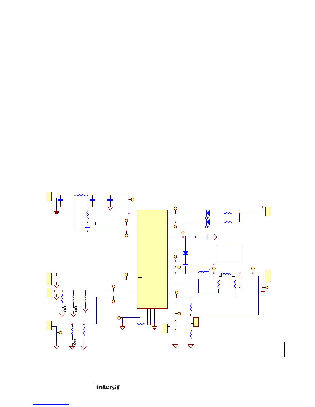
FIGURE 2. ISL9220, ISL9220A EVALUATION BOARD SCHEMATIC
2
February 9, 2012
AN1589.2
Page 3
Evaluation Board Layout
Application Note 1589
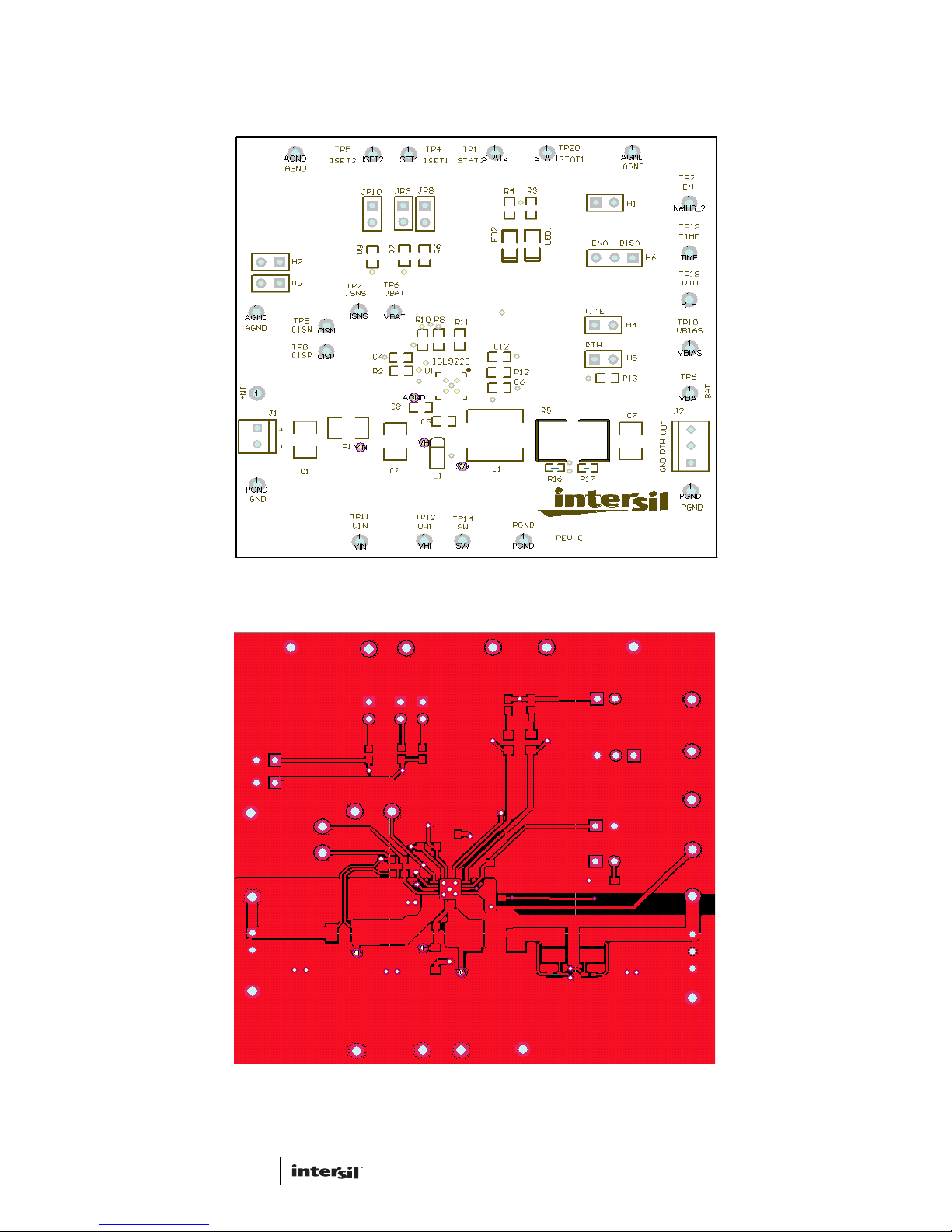
FIGURE 3. SILKSCREEN TOP
ISL9220IRTZEVAL1Z
3
FIGURE 4. TOP LAYER
February 9, 2012
AN1589.2
Page 4
Application Note 1589
Evaluation Board Layout (Continued)
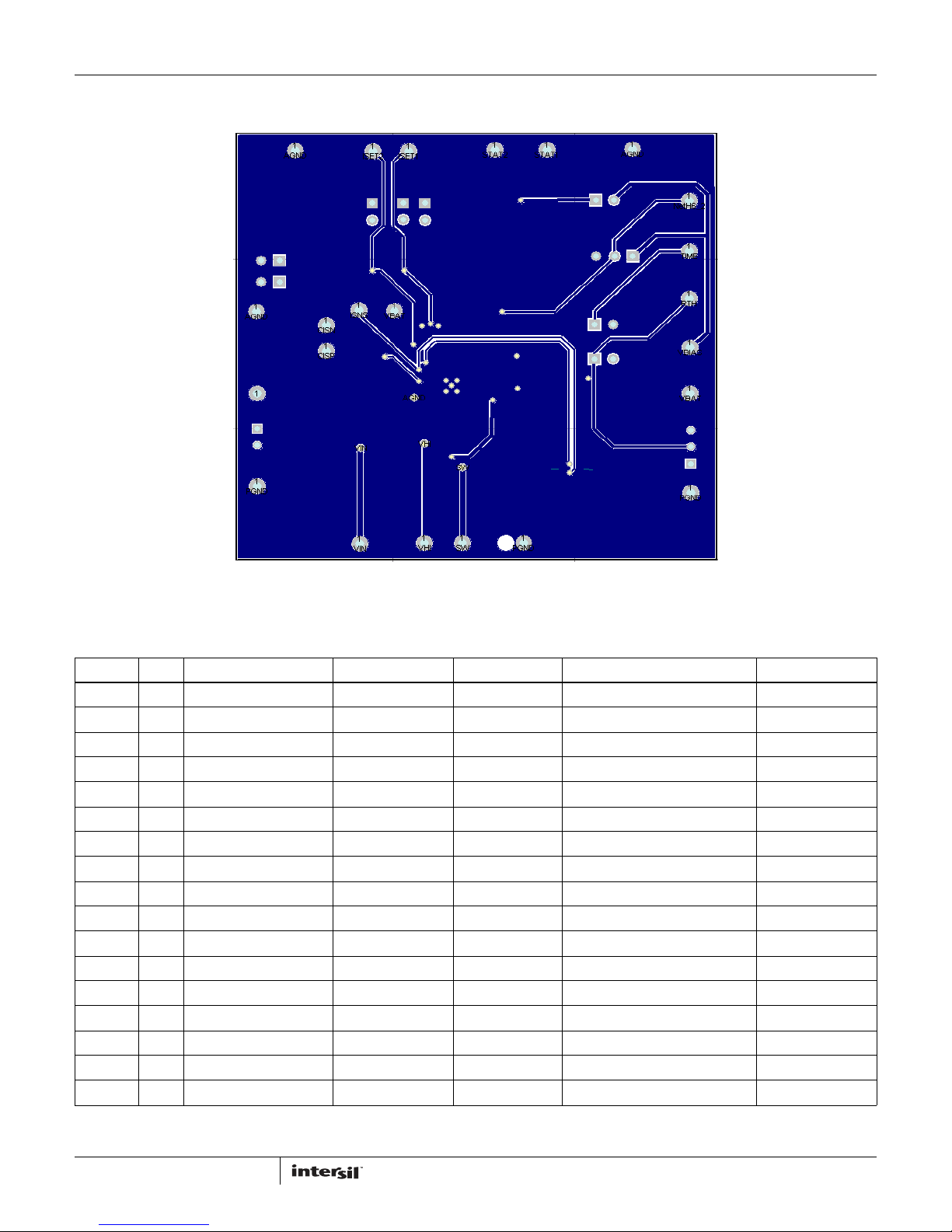
FIGURE 5. BOTTOM LAYER (AGND)
TABLE 1. ISL9220, ISL9220A EVALUATION BOARD BILL OF MATERIALS
ITEM# QTY DESIGNATOR PART TYPE FOOTPRINT DESCRIPTION VENDORS
1 1 R1 0.033Ω 1/3W 1% 1210 P33NACT-ND DIGIKEY
2 1 R2 22 603 RMCF1/1622FRTE-ND DIGIKEY
32 R3, R4 2kΩ 603 311-2.00KHRCT-ND DIGIKEY
4 1 R6 49.9kΩ 603 CR0603-10W4532FT VENKEL
5 2 R7, R8 100kΩ 603 CR0603-16W1003FT VENKEL
6 2 R9, R10 600kΩ 603 CR0603-10W4993FT VENKEL
7 1 R11 0 603 CR0603-16W000T VENKEL
8 2 R12, R13 10kΩ 603 RHM10.0KHTR-ND DIGIKEY
9 1 R5 0.039Ω 1/3W 1% 1210 P39NATR-ND DIGIKEY
10 2 C2, C7 10µF/25V 1210 GRM32DR71E106KA12L MURATA
11 2 C3, C5 0.1µF/25V 603 C1608X7R1H104K TDK
12 1 C4 10nF/50V 603 C1608X7R1H103 TDK
13 1 C6 1.0µF/16V 0805 GRM21BR71C475KA73L MURATA
14 1 C12 15nF/50V 603 GRM188R71H153KA73L MURATA
15 1 D1 RED 0805 67-1552-1-ND DIGIKEY
16 1 D2 GREEN 0805 67-1553-1-ND DIGIKEY
17 1 L1 10µH DR73-100-R 704-DR73-100-R MOUSER
4
February 9, 2012
AN1589.2
Page 5
Application Note 1589
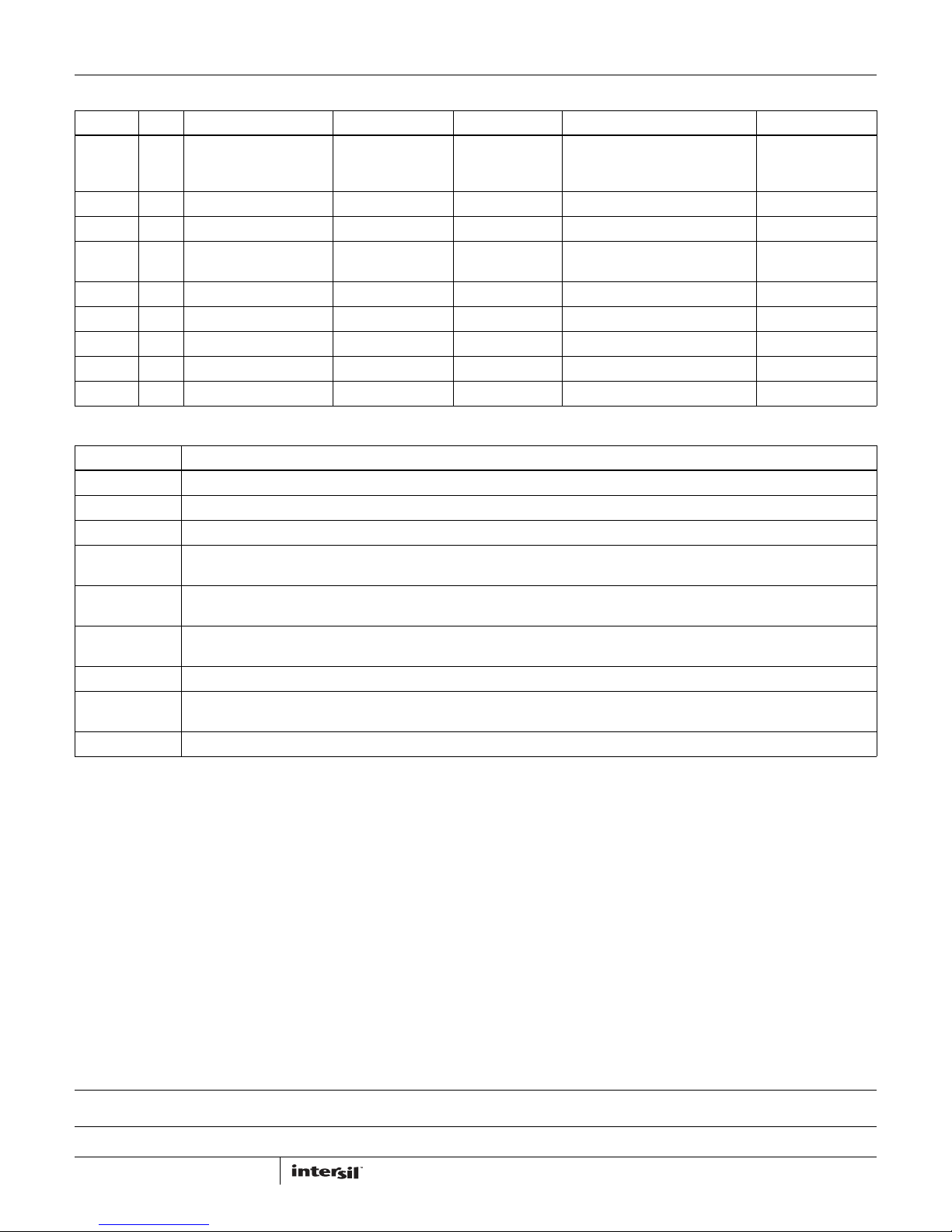
TABLE 1. ISL9220, ISL9220A EVALUATION BOARD BILL OF MATERIALS
ITEM# QTY DESIGNATOR PART TYPE FOOTPRINT DESCRIPTION VENDORS
18 13 TP1, TP2, TP4, TP5, TP7,
TP8, TP9, TP10, TP12,
TP14, TP18, TP19, TP20
19 3 GND, AGND, PGND TEST POINT 2110-00-80-00-00-070 MILL-MAX
20 3 IN+, TP6, TP11 TEST POINT 2110-00-80-00-00-070 MILL-MAX
21 6 JP4, JP5, JP7, JP8, JP9,
JP10
22 1 J1 CONN A1921-ND DIGIKEY
23 1 J2 CONN A19470-ND DIGIKEY
24 1 C1 OPEN 1210
25 2 R16, R17 0 ohm 0402 RMCF0402ZT0R00 STACKPOLE
26 1 U1 4mmx4mm TQFN ISL9220, ISL9220A INTERSIL
JUMPER DESCRIPTION
H1 The jumper installed to connect R3 and R4 to VBIAS pin as power supply to the LED1 and LED2
H2 The jumper installed to short ISET2 pin to ground
H3 The jumper to short ISET1 pin to ground
H4 If a sh unt is i nse rte d on H4, T IME pin is s hor ted to g rou nd, and the TIM EOU T fu nct ion wil l be dis abl ed. I f H4 is o pen , TI MEO UT function
will be enabled and timeout can be set with capacitor at the pin
H5 If a shunt is ins talle d on H5 , VBI AS will be scale d down to 2.5V at the RTH pin by the resistive divider of R12 and R13 and the charger
will operate in normal mode. If H5 is open, RTH pin will be pulled high, and the charger is in suspend mode
H6 It is a 3 pin ju mper. If a shu nt is in sert ed on the l eft two pins, the EN p in is co nnected to grou nd and t he char ger is e nabled. If a shunt
is inserted on the right two pins, the EN pin is connected to VBIAS and the charger is disabled
JP8 Parallels an additional 50kΩ resistor to ISET1 pin such that the charge current will be set at 1.5A with JP9 open
JP9 Parallels an additional 100kΩ resistor to ISET1 pin such that the charge current will be set at 1A with JP8 open. If both JP8 and JP9
are inserted, the charge current will be 2A. If both JP8 and JP9 are open, the charge current will be 500mA
JP10 Parallels an additional 600kΩ resistor to ISET2 pin to set a trickle charge current of 140mA
TEST POINT 2110-00-80-00-00-070 MILL-MAX
CON2 JUMPER 538-22-28-4020 MOUSER
TABLE 2. DESCRIPTION OF JUMPERS
(Continued)
Intersil Corporation reserves the right to make changes in circuit design, software and/or specifications at any time without notice. Accordingly, the reader is
cautioned to verify that the Application Note or Technical Brief is current before proceeding.
For information regarding Intersil Corporation and its products, see www.intersil.com
5
February 9, 2012
AN1589.2
Page 6

Mouser Electronics
Authorized Distributor
Click to View Pricing, Inventory, Delivery & Lifecycle Information:
Intersil:
ISL9220IRTZEVAL1Z
 Loading...