

®
ISL9206
Data Sheet January 5, 2007
FlexiHash+™ For Battery Authentication
The ISL9206 is a highly cost-effective fixed-secret hash
engine based on Intersil’s second generation FlexiHash™
technology. The device authentication is achieved through a
challenge-response scheme customized for low-cost
applications, where cloning via eavesdropping without
knowledge of the device’s secret code is not economically
viable. When used for its intended applications, the ISL9206
offers the same level of effecti v e ness as ot he r si gn i fi ca nt ly
more expensive high-maintenance hash algorithm and
authentication schemes.
The ISL9206 has a wide operating voltage range, and is
suitable for direct powering from a 1-cell Li-Ion/Li-Poly or a
3-cell series NiMH battery pack. The ISL9206 can also be
powered by the XSD bus when the bus pull-up voltage is
3.3V or higher. The device connects directly to the cell
terminals of a battery pack, and includes on-chip voltage
regulation circuit, POR, and a non-crystal based oscillator for
bus timing reference.
Communication with the host is achieved through a singlewire XSD interface - a light-weight subset of Intersil’s ISD bus
interface. The XSD bus is compatible for use with serial ports
offered by all 8250 compatible UART’s or a single GPIO
(general purpose input and output) pin of a microprocessor.
A clone prevention solution utilizing the ISL9206 offers
safety and revenue protection at the lowest cost and power,
and is suitable for protection against after-market
replacement for a wide variety of low-cost applications.
Ordering Information
PART NUMBER
(Note)
ISL9206DHZ-T 206Z -20 to +85 5 Ld SOT-23
ISL9206DRZ-T 06Z -20 to +85 8 Ld 2x3 TDFN
NOTE: Intersil Pb-free plus anneal products employ special Pb-free
material sets; molding compounds/die att ach materials and 100% matte
tin plate termination finish, which are RoHS compliant and com patible
with both SnPb and Pb-free soldering operations. Intersil Pb-free
products are MSL classified at Pb-free peak reflow temperatures that
meet or exceed the Pb-free requirements of IPC/JEDEC J STD-0 20.
PART
MARKING
TEMP.
RANGE (°C)
PACKAGE
(Pb-Free)
Tape and Reel
Tape and Reel
PKG.
DWG. #
P5.064
L8.2x3A
FN9260.2
Features
• Challenge-response based authentication scheme using
32-Bit challenge code and 8-Bit authentication code.
• Fast and flexible authentication process. Multi-pass
authentication can be used to achieve the highest security
level if necessary.
• 16x8 OTP ROM stores up to three sets of 32-Bit
host-selectable secrets with additional programmable
memory for storage of up to 48-Bits of ID code and/or pack
information.
• FlexiHash+ engine uses two sets of 32-Bit secrets for
authentication code generation.
• Non-unique mapping of the secret key to an 8-Bit
authentication code maximizes hacking difficulty due to
need for exhaustive key search (superior to SHA-1).
• Supports 1-cell Li-Ion/Li-Poly and 3-cell series NiMH
battery packs (2.6V ~ 4.8V operation), or powered by the
XSD bus.
• XSD single-wire host bus interface communicates with all
8250-compatible UART’s or a single GPIO. Supports CRC
on read data and transfer bit-rate up to 23kbps.
• True “Zero Power” Sleep mode - automatically entered
after a bus inactivity time-out period
• 5 Ld SOT-23 or 8 Ld TDFN (2mm x 3mm) packages
• -20°C to +85°C operating temperature range
• Pb-free plus anneal available (RoHS compliant)
Applications
• Battery Pack Authentication
• Printer Cartridges
• Add-on Accessories
• Other Non-Monetary Authentication Applications
Related Literature
• Application Note AN1165 “ISL6296 Evaluation Kit”
• Application Note AN1167 “Implementing XSD Host Using
a GPIO”
Pinouts
ISL9206 (8 LD 2X3 TDFN)
TOP VIEW
VSS
1
NC
2
NC
3
VDD
4
• Technical Brief TB363 “Guidelines for Handling and
ISL9206 (5 LD SOT-23)
TOP VIEW
XSD
VSS
N/C
VDD
1
2
3
8
NC
7
NC
6
TIO
5
1
FlexiHash is a trademark of Intersil Americas Inc. All other trademarks mentioned are the property of their respective owners.
5
XSD
4
TIO
CAUTION: These devices are sensitive to electrostatic discharge; follow proper IC Handling Procedures.
1-888-INTERSIL or1-888-468-3774
Processing Moisture Sensitive Surface Mount Devices
(SMDs)”
| Intersil (and design) is a registered trademark of Intersil Americas Inc.
Copyright © Intersil Americas Inc. 2005-2007. All Rights Reserved.
ISL9206
Absolute Maximum Ratings (Reference to GND) Thermal Information
Supply Voltage (VDD) . . . . . . . . . . . . . . . . . . . . . . . . . . . . . . . . 5.5V
All Other Pins. . . . . . . . . . . . . . . . . . . . . . . . . . . . . -0.5 to V
ESD Rating
DD
+0.5V
Human Body Model (Per MIL-STD-883 Method 3015.7) . . .4000V
Machine Model (Per EIAJ ED-4701 Method C-111). . . . . . . .400V
CDM . . . . . . . . . . . . . . . . . . . . . . . . . . . . . . . . . . . . . . . . . .1000V
Recommended Operating Conditions
Ambient Temperature Range. . . . . . . . . . . . . . . . . . .-20°C to +85°C
CAUTION: Stresses above those listed in “Absolute Maximum Ratings” may cause permanent damage to the device. This is a stress only rating and operation of the
device at these or any other conditions above those indicated in the operational sections of this specification is not implied.
NOTE:
is measured with the component mounted on a high effective thermal conductivity test board in free air. See Tech Brief TB379 for details.
1. θ
JA
is measured in free air with the component mounted on a high effective thermal conductivity test board with “direct attach” features. See
2. θ
JA
Tech Brief TB379.
3. For θ
, the “case temp” location is the center of the exposed metal pad on the package underside.
JC
Electrical Specifications Unless otherwise noted, all parameters are guaranteed over the operational supply voltage and temperature
range of the device as follows: T
PARAMETER SYMBOL TEST CONDITIONS MIN TYP MAX UNITS
DC CHARACTERISTICS
Supply Voltage V
During normal operation 2.6 - 4.8 V
DD
During OTP ROM programming 2.8 - 4.8 V
Run Mode Supply Current
(exclude I/O current)
Sleep Mode Supply Current: I
OTP Programming Mode Supply Current I
Internal Regulated Supply Voltage V
Internal OTP ROM Programming Voltage V
POR Release Threshold V
POR Assertion Threshold V
I
VDD = 4.2V - 110 140 μA
DD
VDD = 4.8V - 120 160 μA
DDSVDD
DDP
RG
PP
POR+
POR-
= 4.2V, XSD pin floating - 0.15 0.5 μA
For ~ 1.8ms duration per write operation - 250 500 μA
Observable only in test mode 2.3 2.5 2.7 V
Observable only in test mode 11 12 13 V
XSD PIN CHARACTERISTICS
XSD Input Low Voltage V
XSD Input High Voltage V
XSD Input Hysteresis V
XSD Internal Pull-Down Current I
XSD Output Low Voltage V
XSD Input Transition Time t
XSD Output Fall Time t
XSD Pin Capacitance C
IL
IH
HYS
VDD = 2.6V - 0.8 - μA
PD
V
= 4.2V - 1.2 2.0 μA
DD
V
= 4.8V - 1.8 2.5 μA
DD
OLIOL
X
F
PIN
= 1mA - - 0.4 V
10% to 90% transition time - - 2 μs
90% to 10%, C
XSD BUS TIMING CHARACTERISTICS (Refer to XSD Bus Symbol Timing Definitions Tables)
Programming Bit Rate x = 0.5 to 4 2.89 - 23.12 kHz
XSD Input Deglitch Time T
Pulse width narrower than the deglitch time will not cause
WDG
the device to wake up
= -20°C to +85°C; VDD = 2.6V to 4.8V.
A
LOAD
Thermal Resistance (Typical) θ
(°C/W) θJC (°C/W)
JA
SOT-23 Package (Note 1) . . . . . . . . . . 200 N/A
2x3 TDFN Package (Notes 2, 3) . . . . . 70 10.5
Maximum Junction Temperature (Plastic Package) . . . . . . .+125°C
Maximum Storage Temperature Range. . . . . . . . . .-40°C to +125°C
Maximum Lead Temperature (Soldering 10s) . . . . . . . . . . . .+300°C
1.9 2.2 2.4 V
1.5 1.8 2.1 V
-0.4 - 0.5 V
1.5 - VDD+
0.4V
- 400 - mV
= 12pF - - 50 ns
-6-pF
7-20μs
V
2
FN9260.2
January 5, 2007
ISL9206
Electrical Specifications Unless otherwise noted, all parameters are guaranteed over the operational supply voltage and temperature
range of the device as follows: T
PARAMETER SYMBOL TEST CONDITIONS MIN TYP MAX UNITS
Device Wake-Up Time T
Device Sleep Wait Time T
Auto-Sleep Time-Out Period T
OTP ROM Write Time T
Hash Calculation Time T
Soft-Reset Time T
AC CHARACTERISTICS
Oscillator Clock Frequency f
Charge Pump Clock Frequency f
From falling-edge of break command issued by host to
WKE
falling-edge of break command returned by device
From when the ‘11’ Opcode is detected to the shut-off of
SLP
the internal regulator
From the last transition detected on the XSD bus to the
ASLP
device going into sleep mode
From the last BT of the 2nd write data frame to when
EEW
device is ready to accept the next instruction
From the last BT of the Challenge Code Word from the
HASH
host to the Authentication Code being available for read
From the last BT of the Soft-Reset instruction issued by
SRST
the host to the falling-edge of break command returned
by device
Internal bus reference clock 505 532 560 kHz
OSC
Internal high speed clock (observable only in test mode)
CP
= -20°C to +85°C; VDD = 2.6V to 4.8V. (Continued)
A
35 60 100 μs
4--μs
0.9 - 1.1 s
-1.81.9ms
-1-BT
--30μs
Low-speed mode 3.6 5 6 MHz
High-speed mode 16 20 24 MHz
Pin Descriptions
SOT-23
PIN NUMBER
1 1 VSS System ground.
2 2, 3, 6, 7 NC No connection.
3 4 VDD Supply voltage.
4 5 TIO Production test I/O pin. Used only during production testing. Must be left floating during
5 8 XSD Communication bus with weak internal pull-down to VSS. This pin is a Schmitt-trigger input
PIN NUMBER PIN NAME DESCRIPTION
TDFN
normal operation.
and an open-drain output. An appropriate pull-up resistor is required on the host side.
3
FN9260.2
January 5, 2007
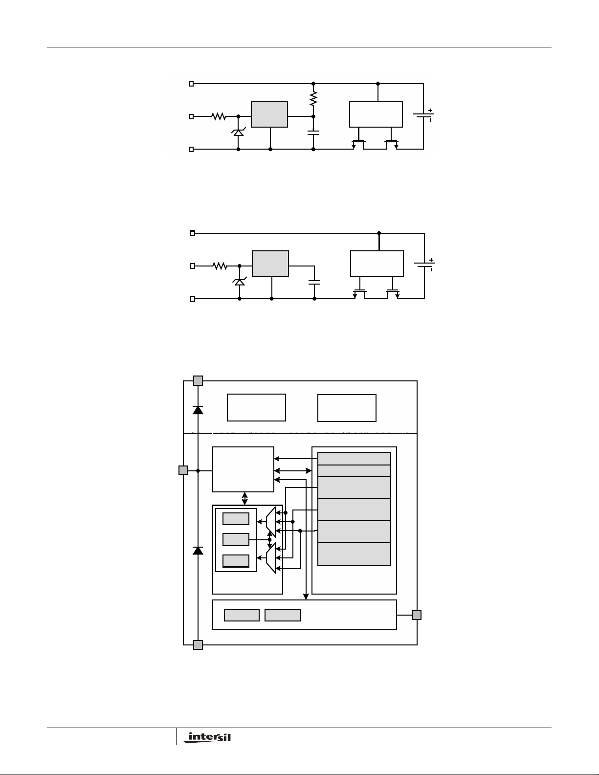
Typical Applications
FIGURE 1. TYPICAL APPLICATION WITH THE ISL9206 POWERED BY THE BATTERY
FIGURE 2. TYPICAL APPLICATION WITH THE ISL9206 POWERED BY THE XSD BUS
PACK+
XSD
PACK-
PACK+
XSD
PACK-
R
100Ω
5.1V
R
100Ω
5.1V
ISL9206
R
1
D
1
1
D
1
VDDXSD
VSS
VDDXSD
VSS
2
100Ω
C
1
0.1µF
C
1
0.1µF
PROTECTIONISL9206
PROTECTIONISL9206
Block Diagram
XSD
VDD
ESD DIODE
COMM
INTERFACE
AUTH
SESL
CHLG
FLEXIHASH+
ENGINE
ESD DIODE
MSCR STAT
POR/2.5V
REGULATOR
XSD
TM
OSCILLATOR
DCFG (1 BYTE)
DTRM (1 BYTE)
SECRET #1
(4 BYTES)
SECRET #2
(4 BYTES)
SECRET #3
(4 BYTES)
GENERAL PURPOSE
(2 BYTES)
16 BYTES
OTPROM
CONTROL/STATUS/
TEST INTERFACE
ANALOG
DIGITAL
TIO
VSS
FIGURE 3. FUNCTIONAL BLOCK DIAGRAM
4
FN9260.2
January 5, 2007
ISL9206
Theory of Operation
The ISL9206 contains all circuitry required to support battery
pack authentication based on a challenge-response
scheme. It provides a 16-Byte One-Time Programmable
Read-Only Memory (OTPROM) space for the storage of up
to 96-Bit of secret for the authentication and other user
information. A 32-Bit hash engine (FlexiHash+™) calculates
the authentication result immediately after receiving a 32-Bit
random challenge code. The communication between the
ISL9206 and the host is implemented through the XSD
single-wire communication bus.
Major functions within the ISL9206 include the following, as
shown in Figure 3.
• Power-on reset (POR) and a 2.5V regulator to power all
internal logic circuits.
• 16 x 8-Bit (16-Byte) OTP ROM as shown in Table 8. The
first part (two bytes) contains the device default
configuration (DCFG) information (such as the device
address and the XSD communication speed) and the
default trimming (DTRM) information (such as the internal
oscillator frequency trimming). The second part contains
two groups (12-Byte) of memory that can be
independently locked out for the storage of up to three
sets of secret. The last part provides two additional bytes
of space for general-purpose information.
• Control functions, including master control (MSCR) and
status (STAT) registers (as shown in Table 9), interrupt
generation, and the test-related interface.
• FlexiHash+™ engine that includes the 32-Bit highly nonlinear proprietry hash engine, secret selection register,
challenge code register, and the authentication result
register. Table 10 shows all the registers.
• XSD communication bus Interface. The XSD device
address and the communication speed are configured in
the DCFG address in the OTPROM, as given in Table 8.
• Time Base Reference.
The following explain in detail the operation of the ISL9206.
Power-On Reset (POR)
The ISL9206 powers up in Sleep mode. It remains in Sleep
mode until a power-on ‘break’ command is received from the
host through the XSD bus. The initial power-on ’break’ can
be of any pulse width as long as it is wider than the XSD
input deglitch time (20μs). Once the ‘break’ command is
received, the internal regulator is powered up. About 20μs
after the falling edge of the power-on ‘break’, an internal
POR circuit releases the reset to the digital block, and a
POR sequence is started. During the POR sequence, the
ISL9206 initializes itself by loading the default device
configuration information from pre-assigned locations within
the OTP ROM memory. After initialization, a ‘break’
command is returned to the host to indicate that the ISL9206
is ready and waiting for a bus transaction from the host.
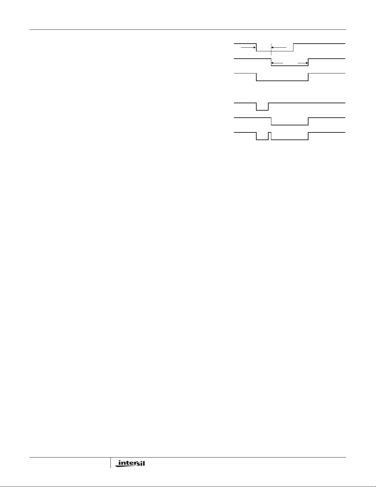
HOST BREAK
DEVICE BREAK
XSD BUS
WAVEFORM
(A) WHEN THE HOST POWER-ON BREAK IS WIDER THAN 60µs.
HOST BREAK
DEVICE BREAK
XSD BUS
WAVEFORM
(B) WHEN THE HOST POWER-ON BREAK IS NARROWER THAN 60µs.
FIGURE 4. POWER-ON BREAK SIGNAL TO WAKE-UP THE
ISL9206 FROM SLEEP MODE
60µs
TYP
1.391
BT
D
Note that the ISL9206 will initiate the power-on sequence
without waiting for the power-on ‘break’ signal to return to
the high state. If the host sends an initial ‘break’ pulse wider
than 60μs, the device-ready ‘break’ returned by the ISL9206
will likely be merged with the pulse sent by the host and,
therefore, may not be detectable. Figure 4 illustrates the
waveforms during the Power-on Reset. Figure 4 (A)
represents the case when the power-on ‘break’ rising edge
occurs after the device starts sending the ‘break’. Figure 4
(B) represents the case when the power-on ‘break’ finishes
before the device sends its ‘break’. The device break signal
is always 1.391 times of the device bit-time (BT, see XSD
Bus Interface section for more details). Either case in Figure
4 will wake up the device successfully if the device is in the
sleep mode.
It is important to keep in mind that a narrow ‘break’ signal will
be taken as a normal bit signal and cause errors, if the
device is not in the sleep mode. For this reason, the narrow
power-on ‘break’ signal should be used only if the user has
to see the returned ‘break’ signal.
Auto-Sleep
While the ISL9206 is powered up and there is no bus activity
for more than about 1 second, the device will automatically
return to Sleep mode. Sleep mode can be entered
independent of whether the XSD bus is held high or low.
While the ISL9206 is in Sleep mode, it is recommended that
the XSD bus be held low to eliminate current drain through
the XSD-pin internal pull-down current.
Auto-Sleep mode can be disabled by clearing the ASLP bit
in the MSCR register. By default, Auto-Sleep is always
enabled at power-up and after a soft reset. Auto-sleep
function can be permanently disabled by clearing the 0-00[2]
bit (the ASLP bit in DCFG) during OTP ROM programming.
5
FN9260.2
January 5, 2007

ISL9206
OTP ROM
The 16-Byte OTP ROM memory is based on EEPROM
technology and is incorporated into the ISL9206 for storage
of non-volatile information. OTP ROM contents (refer to
Table 8) can include but not limited to:
1) Device default settings (address 0-00)
2) Factory programmed trim parameters (address 0-01)
3) Device authentication secrets (address 0-02 to 0-0D)
4) Pack information and ID (address 0-0E and 0-0F)
The memory can be written multiple times before two lock-
out bits (SLO[1:0] in DCFG, see Table 8) being set. The
SLO[1] (bit 1) locks out the memory between 0-02 and 0-09
and the SLO[0] (bit 0) locks out the memory between 0-0A to
0-0D. These two bits can be set independently. Prior to lockout, the memory can be written and read directly through the
XSD bus interface. After lock-out, writing to all ROM
addresses and reading from secret code locations will be
permanently disabled after performing a reset cycle.
Writing to the EEPROM requires the supply voltage at the VDD
pin be maintained at a minimum of 2.8V. Failure to do so may
result in unreliable ROM programming or total write failure.
The OTP ROM must be written two bytes at a time, but 2, 4
or 16-Bytes of data can be read by the host in a single bus
transaction. Only even addresses are allowed in OTP ROM
read/write. A 16-Byte read with CRC allows the entire ROM
content to be quickly verified by simply checking the CRC
byte. The DTRM address stores the default trimming
parameters and is a read-only address. The DCFG and
DTRM (0-00 and 0-01 addresses) need be written
simultaneously but the data to the DRTM address is ignored.
The OTP ROM writing process takes approximately 1.8ms
per two-byte. While the write process is taking place, no bus
transaction is allowed. Attempt to access the ISL9206 during
an on-going write process will result in the device ignoring
the access instruction and issuing an interrupt to the host.
The OTP ROM programming is register-based, and may be
performed at the pack manufacturer’s facility.
Device Control and Status
The ISL9206 has a control and a status register. The control
register can be read and written by the host but the status
register is read only. Both registers contain the device
configuration information (see Table 9). The status register
also contains the device status information that may lead to
an interrupt signal to the host.
Following a host-initiated power-on ‘break’ signal or soft
reset command, the ISL9206 will configure its default mode
of operation based on information stored within DCFG
address of the OTP ROM. The default configuration is
loaded into the master control (MSCR) and the status
(ST AT) registers. Functions that are configured by OTP
ROM settings include:
a) device address (DAB[1:0])
b) XSD bus speed (SPD[1:0])
c) register default settings (eINT and ASLP)
d) ROM read/write lock-out (SLO[1:0])
The ISL9206 incorporates interrupt functions to allow the
host to be quickly informed of device status and error
conditions. Available interrupts are summarized in T able 1.
When an interrupt enable bit is set, a ’break’ command is
sent to the host whenever its corresponding interrupt status
bit is set. After this, the host should read the STAT register
immediately. If the following instruction frame from the host
does not access the STAT register, another ‘break’ will be
sent immediately after receiving the full instruction frame.
This process is repeated until the host reads from the STAT
register. Upon reading of the ST AT register, all status bits will
be cleared.
Refer to the MSCR and STAT register descriptions for
detailed explanation of the interrupt functions.
FlexiHash+™ Engine
The FlexiHash+™ engine contains a 32-Bit highly non-linear
proprietry hash engine and three registers. T able 10 lists the
three registers. The 1-Byte secret selection (SESL) register
select two sets of secret (32-Bit each) from the OTP ROM to
program the hash engine. The 4-Byte challenge code
register (CHLG) receives the challenge code from the host
through the XSD bus. Once the challenge code is received,
the hash engine generates a 1-Byte authentication result
code and stores in the AUTH register for the host to read.
Figure 5 shows the data flow of the authentication process.
The following sections describe the authentication process
and FlexiHash+™ encoding scheme in detail.
THE DEVICE AUTHENTICATION PROCESS
To start an authentication process, the host sends a ‘break’
command to wake up the ISL9206. Then host writes to the
SESL register to select the two sets of secrets to be used for
authentication code generation. After that, the host
generates a pseudo-random 4-Byte challenge code to input
into the CHLG register to initiate the authentication process.
Upon receiving the fourth byte of the challenge code, the
ISL9206 immediately starts computing the authentication
code. Once the computation is completed, the 8-Bit
authentication code is made available at the AUTH register
for the host to read out. The host reads this code and,
concurrently, calculates the correct authentication code
based on the challenge code it generated and the same
secrets chosen, and finally compares the result with the
authentication code read from the device. If the codes do not
match up, the device is a fake device and the host may shut
itself down. The flow chart in Figure 6 summarizes the above
process that the host needs to execute.
6
FN9260.2
January 5, 2007

ISL9206
START
WAKE UP ISL9206 USING A
REGULAR BREAK SIGNAL
+
FIGURE 5. AUTHENTICATION PROCESS FLOW DIAGRAM
It is recommended that device authentication be done once
in a while to maximize its effectiveness. Before a new
challenge code can be accepted by the device, the SESL
register must be re-written again to ensure that the original
seeds are re-loaded from the OTP ROM into the hash
engine prior to performing the next authentication code
calculation. Failure to follow the sequence will result is a bus
error, causing the sBER flag to be set in the STAT register.
SET-UP FOR DEVICE AUTHENTICATION SUPPORT
To configure the host and the ISL9206 to support device
authentication function, the pack manufacturer will need to
select at least 2 sets of 32-Bit secret codes. For greater
security, a third set of 32-Bit secret may be used. The
FlexiHash+™ engine requires two sets of 32-Bit secrets for
use in its hash calculation: the first set to define its hash
function, and the second set to initialize its seed for hash
calculation. These two sets can be selected from the same
secret location. The chosen secret codes are to be kept by
the pack manufacturer and maintained at utmost
confidentiality.
After the secrets have been determined, they are written into
the device’s OTP ROM. After verification that the codes have
been written in correctly, the relevant secrets lock-out bits at
ROM address location 0-00 should be set. Once set, the
lock-out bits can no longer be cleared. Thereafter, read/write
access to the secret information will no longer be possible,
and the secret codes are made available only to the
FlexiHash+™ engine for generation of authentication code
based on a challenge code input from the host.
SELECT HASH FUNCTION AND SEED
BY WRITING TO SESL REGISTER
SEND A 32-BIT RANDOM
CHALLENGE TO CHLG REGISTER
READ THE AUTHENTICATION
RESULT FROM AUTH REGISTER,
AFTER WAITING FOR 1 BT
CALCULATE THE EXPECTED
AUTHENTICATION RESULT
BASED ON THE SAME SECRETS
THE TWO RESULTS MATCH?
YES
END
FIGURE 6. FLOW CHART FOR AUTHENTICATION PROCESS
D
NO
SHUT DOWN
THE SYSTEM
THE HASH ENGINE
The hash engine consists of a cascade of programmable
highly non-linear proprietry encoders. Details on the
proprietry encoder implementation will be made available to
users under NDA only.
On the host side, the same secret codes will need to be kept,
and the same FlexiHash+™ engine will have to be
implemented in firmware. It is important that the secret
codes be stored scrambled in the host’s non-volatile memory
so that the secret information cannot be easily revealed by
monitoring signal transfer on the host PCB.
7
FN9260.2
January 5, 2007

ISL9206
XSD Host Bus Interface
Communication with the host is achieved through XSD, a
light-weight subset of Intersil’s ISD single-wire bus interface.
XSD is a programmable-rate pseudo-synchronous
bidirectional host-initiated instruction-based serial
communication interface that allows up to two slave devices
to be attached and addressed separately. It includes
features to enable quick and reliable communication. The
communication protocol is optimized for efficient transfer of
data between the device and the host. The list below
outlines the features supported by the XSD bus interface:
• Programmable bit rate up to 23kbps
• Up to 2 devices can be connected to the host and
addressed separately
• 16-Bit host instruction frame supports multi-byte register
read and write
• Built-in communication error detection
• CRC generation capability
• Supports interrupt signaling
• Integrated bus inactivity detector for automatic activation
of sleep mode
XSD BUS PHYSICAL MODEL
The physical model of the XSD bus is shown in Figure 7.
The model shows a single-wire connection between the host
and the device, not including the ground signal. The input
logic on the device side is designed to be compatible with
any voltage between 1.8V to 5.0V . The host interface should
contain an open-drain or open-collector output. The pull-up
resister R
voltage V
the host supply voltage should be used for pull-up.
DATA TRANSFER PROTOCOL
To initiate a transaction, the host first sends a 16-Bit
instruction frame to the device, followed by data byte
frame(s) if the instruction is a write operation. The instruction
frame consists of a chip-select code, operation code,
register bank and address pointer, and number of data bytes
information, as shown in Figure 9. If the instruction is a read
operation, the device will return 1 to 17 byte frames of data
can be connected either to the host supply
PU
or the device supply voltage V
DDH
DDD
. Typically
back to the host. The serial data transfer always takes place
with the LSB first. The following explains the bus symbols
and the transaction frames are introduced in later sections.
BUS SIGNALING SYMBOLS
The XSD bus is nominally held high. Various bus symbols
and commands are generated by active-low pulse width
modulation. Following are the set of valid bus signaling
symbols supported by the XSD interface:
1) break (issued by host):
• used to wake the device up from Sleep mode (Note: a
narrow ‘break’ can also be used to wake up the device
from the Sleep mode, as described in the Power-on Reset
section)
• used to reset the device’s XSD bit counters and time
qualifiers
• used to signal a change in communication channel (from
one slave device to another)
2) break (issued by device):
• used as ‘device-ready’ indication to the host (after a
Soft-reset or wake up from Sleep mode)
• used as an interrupt indicator
3) ‘1’ symbol:
• used for instruction and data coding
4) ‘0’ symbol:
• used for instruction and data coding
SYMBOL TIMING DEFINITIONS
Symbol timings are defined in terms of bit-time (BT),
determined by the selected bus transfer bit-rate
pre-programmed into the device’s OTP ROM location
0-00[5:4]. Selectable bus speeds are: 2.89kHz (x = 0.5),
5.78kHz (x = 1), 11.56kHz (x = 2) and 23.12kHz (x = 4).
An instruction or data frame consists of a sequence of ‘1’
and/or ‘0’ symbols. Figure 8 illustrates the timing definitions.
A ‘1’ symbol is nominally 0.3 BT wide while a ‘0’ symbol is
nominally 0.7 BT wide. One ‘1’ or ‘0’ symb ol is represented
in each BT period. Any detected pulse width less than 0.124
BT wide will be interpreted as a glitch and will result in a bus
error. Table 2 and 3 summarize the timing definitions of all
TABLE 1. INTERRUPT EVENT SUMMARY
INTERRUPT
CONDITION
OTP ROM Write-inProgress
XSD Bus Error eINT sBER XSD bus error or invalid instruction frame detected. Improper authentication sequence
Register Access
Error
ENABLE BIT
eEEW
(fixed)
eINT sACC Accessing protected registers.
INTERRUPT
STATUS FLAG INTERRUPT EVENT
sEEW Accessing the ISL9206 during an on-going ROM write process (used only during initial
OTP ROM programming).
detected.
8
FN9260.2
January 5, 2007

ISL9206
HOST
TX
RX
XSD
V
DDD
ESD
Diode
6pF
1.5μA
ESD
Diode
Open-Drain
Port Pin
V
DDH
R
PU
FIGURE 7. THE CIRCUIT MODEL FOR THE XSD SERIAL BUS
tb
t0
t1
tg
glitch
10 Break
BT
FIGURE 8. THE BUS SIGNAL TIMING DIAGRAM
DEVICE
RX
TX
TABLE 2. HOST TIMING DEFINITIONS OF SYMBOLS AND BUS SIGNALING
PARAMETER SYM DESCRIPTION MIN TYP MAX UNIT
Bit Time BT
x = 0.5, 1, 2, or 4 173.6/x μs
H
Deglitch period tg PW (Pulse Width) less than this will result in a frame error 0.124 BT
‘1’ pulse width t1
‘0’ pulse width t0
‘break’ time tb
PW in this range will be interpreted as a ‘1’ code 0.227 0.453 BT
H
PW in this range will be interpreted as a ‘0’ code 0.591 0.824 BT
H
PW in this range will be interpreted as a ‘break’ command 1 100 BT
H
NOTE: Unless otherwise stated, all pulse width (PW) referenced are with respect to an active-low pulse.
TABLE 3. DEVICE TIMING DEFINITIONS OF SYMBOLS AND BUS SIGNALING
PARAMETER SYM DESCRIPTION MIN TYP MAX UNIT
Bit Time BT
‘1’ pulse width t1
‘0’ pulse width t0
‘break’ time tb
x = 0.5, 1, 2, or 4 164.2/x 172.8/x 181.4/x μs
D
‘1’ code transmit pulse width 0.304 BT
D
‘0’ code transmit pulse width 0.696 BT
D
PW in this range will be interpreted as a ‘break’ command 1.391 BT
D
H
H
H
H
D
D
D
9
FN9260.2
January 5, 2007

ISL9206
015
015
015
OPCODEBANKADDRESSBYTES CS
OPCODEBANKADDRESSBYTES CS
OPCODEBANKADDRESSBYTES CS
FIGURE 9. THE 16-BIT INSTRUCTION FRAME FIELD DEFINITION
TABLE 4. DEFINITION OF THE OPCODE FIELD
OPCODE DESCRIPTION ACTION
00 Write Operation Write to device register
01 Read Operation (normal) Read from device register
10 Read Operation (with CRC) Read from device register. Append 1-Byte CRC to the end of the last read frame.
11 Sleep Mode Activation Immediately sets the device in Sleep mode.
Note: After detecting the ‘11’ Opcode, the device immediately enters sleep mode. If more than 3
bits sent, subsequent pulses may wake the device up again.
Access Instruction Frame
The XSD access instruction frame is shown in Figure 9. The
instruction frame consists of 16 bits of digital signal with the
contents described as following.
CS FIELD
The CS field is a 1-Bit Chip Address Selection. An initial
1-Bit Chip Address code of ‘0’ is pre-programmed into the
device’s OTP ROM address location 0-00[7:6] at the time of
chip manufacture, and may be re-programmed by the pack
manufacturer if needed. If the CS code in the instruction
does not match the device’s Chip Address code, the
instruction, and any subsequent frames that follow, will be
ignored until a break command is received.
OPCODE FIELD
The OPCODE is a 2-Bit field defines the operation of the
transaction following the instruction frame. The operations
are described in Table 4.
BANK FIELD
The memories in the ISL9206 are divided into four banks.
The BANK field is defined in Table 5.
TABLE 5. BANK FIELD DEFINITION.
BANK MEMORY/REGISTER BANK SELECTION
00 OTP ROM
01 Control and Status Registers
10 Device Authentication Registers
11 Test Registers (Reserved)
ADDRESS FIELD
The address field indicates the starting address of a memory
or register read or write sequence. Keep in mind that only odd
starting addresses are allowed for the OTP ROM access.
BYTES FIELD
The bytes field indicates the number of data bytes to read or
write, not including the CRC byte. Not all BYTES Field
settings are supported. Only settings marked with an ‘X’ is
valid for a particular bus instruction, as indicated in Table 6.
Attempt to read or write with an invalid BYTES setting may
yield unpredictable results.
Writing to OTP ROM can occur at only two bytes at a time,
but reading from OTP ROM can happen at 2, 4 or 16 bytes
at a time. Writing to and reading from OTP ROM in any other
byte denomination will yield unpredictable result, and should
therefore be strictly prohibited.
TABLE 6. DEFINITION OF THE BYTES FIELD
BYTES
FIELD
5 - 6 N/A Invalid selection. Causes a bus error.
DATA BYTES
TO FOLLOW
0 0 Invalid selection. Causes a bus error.
1 1 X Must use 1-Byte read for clearing of the STAT register.
22XXX
3 N/A Invalid selection. Causes a bus error.
44 X X
7 16 X For reading from OTP ROM only (prior to lock-out).
OTP ROM
WRITE
OTP ROM
READ
REG READ
OR WRITE
CHLG CODE
WRITE COMMENTS
10
FN9260.2
January 5, 2007

ISL9206
Bus Transaction Protocol
The XSD bus for the ISL9206 defines three types of bus
transactions. Figure 10 shows the bus transaction protocol.
The blue color represents the signal sent by the host and the
green color stands for the signal sent by the device. Before
the transaction starts, the host should make sure that the
XSD device is not in the sleep mode. One method is to
always send a ‘break’ signal before starting the transaction,
as shown in Figure 10. If the device is not in the sleep mode,
the ‘break’ signal is not mandatory. The ‘break’ pulse width
may appear to be wider than what the host sends out
because of the reason explained in Figure 4. The symbols in
Figure 10 are explained in Table 7.
TABLE 7. SYMBOLS IN THE BUS TRANSACTION PROTOCOL
SYM DESCRIPTION MIN TYP MAX
IFG
Host inter-frame gap 0 BT
H
IFG
Device inter-frame gap 1 BT
D
TAHHost turn-around time 1 BT
TA
Device turn-around time 1 BT
D
(A) Multi-Byte Write Instruction.
break
T
SD
Write Instruction Frame
H
H
800ms
D
800ms
D
Passive CRC Support
The CRC feature only supports the read transaction in the
ISL9206. When the OPCODE in the instruction is ‘10’, an
8-Bit CRC is automatically calculated for the data bytes
being transferred out. The CRC result is then appended after
the last data byte is read out.
CRC is generated using the DOW CRC polynomial as
follows:
Polynom = 1 + X
The CRC generation algorithm is logically illustrated in
Figure 11. Prior to a new CRC calculation, the LFSR (linear
feedback shift register) is initialized to zero. The read data to
be transmitted out is concurrently shifted into the CRC
calculator. After the actual data is transmitted out, the final
content of the LFSR is the resulting CRC value. This value is
transmitted out after the read data, with LSB being
transmitted out first.
IFG
H
Data Frame 1
4
+ X5 + X8
IFG
H
Data Frame 2
(B) Multi-Byte Read Instruction.
break
T
SD
(C) Back-to-Back Transaction (Read Followed by Write).
break
T
SD
FIGURE 10. XSD BUS TRANSACTION PROTOCOL. THE ‘BREAK’ SIGNAL IS OPTIONAL IF THE DEVICE IS AWAKE
Read Instruction Frame
Read Instruction Frame
TA
D
TA TA
D
Data Frame 1
(output from slave)
Data Frame
(output from slave)
1st
Stage
LSB MSB
2nd
Stage
3rd
Stage
4th
Stage
5th
Stage
6th
Stage
Stage
7th
IFG
D
D
(output from slave)
Next Instruction
H
H
8th
Stage
Data Frame 2
Frame
Serial
Serial
Output
Data
FIGURE 11. THE CRC CALCULATOR FOR THE PASSIVE CRC SUPPORT
11
FN9260.2
January 5, 2007

ISL9206
Analog Biasing Components and Clock
Generation
The analog section in the ISL9206 mainly includes the Time
Base Generator and the internal regulator for powering the
circuits in the ISL9206.
TIME BASE GENERATOR
A time base generator is included on-chip to provide timing
reference for serial data encoding and decoding at the XSD
bus interface. This eliminates the need for an external
crystal. The time base oscillator is trimmed during
manufacturing to a nominal frequency of 532.5kHz. It has a
frequency tolerance better than 5% over operating supply
voltage and temperature range.
INTERNAL VOLTAGE REGULA TOR
The ISL9206 incorporates an internal voltage regulator that
maintains a nominal operating voltage of 2.5V within the
device. The regulator draws power directly from the VDD
input. No external component is required to regulate circuit
voltage. The regulator is shut off during Sleep mode.
Memory/Operational Register Description
The ISL9206 memory and register structure is organized into
4 banks of 256 addressable locations. However, not all of the
addressable registers are used nor implemented. Accessing
an unimplemented register will result in the access
instruction being ignored. A bus error indication may or may
not be flagged.
Bank 0 is dedicated for the OTP ROM. There are 16 memory
locations implemented in the array. Writing to the OTP ROM
has no immediate effect on the chip operation until a
Power-on Reset occurred, or a soft reset is issued. Table 7
describes the OTP ROM memory assignment. The default
factory setting for address [0:00] is given in Table 11.
Bank 1 contains the Control and Status registers. Only 2
registers are implemented. Table 8 shows the register map
of the Bank 1 registers. Detailed description of register
settings is given in Table 14 and 15.
Bank 2 contains the Authentication registers. Only 3
registers are implemented. These registers are used during
the battery pack authentication process. Table 10 describes
the mapping of the Authentication registers.
Bank 3 is reserved for Intersil production testing only, and
will not be accessible during normal operation. Accessing
the Test and Trim Registers when not in test mode will result
in a bus error.
TABLE 8. OTP ROM MEMORY MAP (BANK 0)
ADDRESS NAME DESCRIPTION BIT 7 BIT 6 BIT 5 BIT 4 BIT3 BIT 2 BIT 1 BIT 0
0-00 DCFG Default Configuration DAB[1:0] SPD[1:0] eINT ASLP SLO[1:0]
0-01 DTRM Default Trimming HSF TIBB[2:0] TOSC[3:0]
0-02 SE1A Auth Secret #1A S1A[7:0]
0-03 SE1B Auth Secret #1B S1B[7:0]
0-04 SE1C Auth Secret #1C S1C[7:0]
0-05 SE1D Auth Secret #1D S1D[7:0]
0-06 SE2A Auth Secret #2A S2A[7:0]
0-07 SE2B Auth Secret #2B S2B[7:0]
0-08 SE2C Auth Secret #2C S2C[7:0]
0-09 SE2D Auth Secret #2D S2D[7:0]
0-0A SE3A Auth Secret #3A S3A[7:0]
0-0B SE3B Auth Secret #3B S3B[7:0]
0-0C SE3C Auth Secret #3C S3C[7:0]
0-0D SE3D Auth Secret #3D S3D[7:0]
0-0E INF1 General Purpose General purpose non-volatile memory for storage of model ID, date code, and other
0-0F INF2 General Purpose
NOTE: Information stored in address 0-0E (INF1) and 0-0F (INF2) is for use by the host firmware only. Actual content depends on the host firmware
customization preference.
cell information
12
FN9260.2
January 5, 2007

ISL9206
TABLE 9. CONTROL AND STATUS REGISTERS (BANK 1)
ADDRESS NAME DESCRIPTION BIT 7 BIT 6 BIT 5 BIT 4 BIT3 BIT 2 BIT 1 BIT 0
1-00 MSCR Master Control eEEW eINT -- -- -- -- ASLP SRST
1-01 STAT Device Status sEEW sBER sACC -- DAB[1:0] SLO[1:0]
TABLE 10. AUTHENTICATION REGISTERS (BANK 2)
ADDRESS NAME DESCRIPTION BIT 7 BIT 6 BIT 5 BIT 4 BIT3 BIT 2 BIT 1 BIT 0
2-00 SESL Secrets Selection -- -- -- -- CSL[1:0] SSL[1:0]
2-01 CHLG Challenge Code Register CHLG[31:0]
2-05 AUTH Authentication Code Register AUTH[7:0]
TABLE 11. DEFAULT CONFIGURATION (DCFG) REGISTER SETTINGS
BIT NAME TYPE DEFAULT DESCRIPTION
7:6 DAB[1:0] RW
5:4 SPD[1:0] RW
3eINT RW
2ASLP RW
1:0 SLO[1:0] RW
00 Device Address Bit Setting:
00 : device responds only when CS field in instruction frame is’0’
01 : device responds to any CS field value in instruction frame
10 : device responds to any CS field value in instruction frame
11 : device responds only when CS field in instruction frame is ‘1’
01 XSD Bus Speed Setting: Configures the bit rate of the XSD bus interface.
00 : 0.5x (2.89kbps)
01 : 1x (5.78kbps)
10 : 2x (11.56kbps)
11 : 4x (23.12kbps)
1 Power-on default setting of eINT bit in the MSCR register.
1 Power-on default setting of ASLP bit in the MSCR register.
00 Secrets Lock-out Bits:
Bit 1 : Read/Write lock-out bit for address locations 0-02 to 0-09 (Secret Set #1 & #2)
Bit 0 : Read/Write lock-out bit for address locations 0-0A to 0-0D (Secret Set #3)
NOTE: Once Bit 0 or Bit 1 is set, writing to the OTP ROM will permanently be disabled
(after a reset cycle).
TABLE 12. DEFAULT TRIMMING (DTRM) REGISTER SETTINGS
BIT NAME TYPE DEFAULT DESCRIPTION
7HSF R 0Unused
6:4 TIBB[2:0] R -- Reference Current Trim Setting
3:0 TOSC[3:0] R -- Oscillator Frequency Trim Setting
TABLE 13. LEGEND FOR THE TYPE COLUMN
TYPE READ ACTION WRITE ACTION
R Read-only Data read Data ignored
W Write-only Zeros read Data written
RW Read/Write Data read Data written
RC Clear after read Data read, then
WC Clear after write Zeros read Data written, then
<> Default setting loaded from designated OTP ROM bit
locations
W
Writing disabled after lock-out
cleared
Data ignored
cleard
ADDRESS 0-00: DEFAULT CONFIGURATION (DCFG)
This address location stores the default configuration when
the ISL9206 is manufactured. Table 11 describes each bit in
detail. The legend for the TYPE column is given in Table 13.
ADDRESS 0-01: DEFAULT TRIM SETTING (DTRM)
This address location is writable only when the device is in
test mode. During normal operation, any data written to it will
be ignored. Tab le 12 describes the DTRM address in detail.
ADDRESS 0-02/03/04/05: AUTHENTICATION SECRET
SET #1 (SE1A/B/C/D)
These address locations store the first set of secrets to be
used for hash calculation. Reading and writing to this
register can be disabled by setting the SLO[1] bit at OTP
ROM location 0-00[1].
13
FN9260.2
January 5, 2007

ISL9206
ADDRESS 0-06/07/08/09: AUTHENTICATION SECRET
SET #2 (SE2A/B/C/D)
These address locations store the second set of secrets to
be used for hash calculation. Reading and writing to this
register can be disabled by setting the SLO[1] bit at OTP
ROM location 0-00[1].
ADDRESS 0-0A/0B/0C/0D: AUTHENTICATION SECRET
SET #3 (SE3A/B/C/D)
These address locations store the optional third set of
secrets to be used for hash calculation. Reading and writing
to this register can be disabled by setting the SLO[0] bit at
OTP ROM location 0-00[0].
Alternately, this memory space can be used to store
additional cell information which can be accessed by the
host. In this case, the SLO[0] bit should not be set.
TABLE 14. MASTER CONTROL REGISTER (MSCR)
BIT NAME TYPE DEFAULT DESCRIPTION
7eEEW R 0
<1/0>
6eINT RW 0
<1>
5:2 -- R 0 Unused.
1ASLP RW 0
<1>
0 SRST WC 0 Soft Reset: When a ‘1’ is written, and all registers are reset to their default states, all bus counters
OTP ROM Write-in-Progress Interrupt Enable: When enabled, it allows the sEEW bit to flag an
interrupt whenever the sEEW bit is set by its interrupt event. The eEEW bit is fixed at ‘1’ when none
of the OTP ROM lock-out bits is set. When any or both of the lock-out bits are set, the eEEW bit
will become permanently ‘0’ after a reset.
Global Interrupt Enable: When enabled, it allows the sBER or sACC bit to flag an interrupt to the
host whenever any of the respective interrupt event occurred.
(Default setting loaded from OTP ROM location 0-00[3])
Auto Sleep Mode enable: When set, the ISL9206 will automatically enter Sleep mode after about
1s of XSD bus inactivity. When cleared, the device can only enter Sleep mode on Opcode
command.
(Default setting loaded from OTP ROM location 0-00[2])
and timers are reset to their start-up conditions, and device configuration information is reloaded
from OTP ROM. After the reset sequence is completed, a ‘break’ pulse is sent to the host.
TABLE 15. DEVICE STATUS REGISTER (STAT)
BIT NAME TYPE DEFAULT DESCRIPTION
7 sEEW RC 0 OTP ROM Write-in-Progress Flag: This bit is set when attempt is made by the host to read from
or write to the ISL9206 while the ROM is still processing the previous write instruction.
6 sBER RC 0 XSD Bus Error Flag: This bit is set when one or more of the following occurred at the bus interface:
a) An invalid pulse width is received
b) Bus activity is detected before the device completes its power-up sequence
c) An invalid BYTES field in the instruction frame
d) Improper authentication sequence is detected
e) Reading secret information after the corresponding lock-out bits are set
5 sACC RC 0 Register Access Error Flag: This bit is set whenever an instruction frame attempts to access a
protected register as follows:
a) Writing to OTP ROM after the ISL9206 has been locked out (any or both of the lock-out bits set)
b) Accessing the ISL9206ís Test and Trim Registers when the device is not in test mode
4-- R 0Unused
3:2 DAB[1:0] R 00
<00>
1:0 SLO[1:0] R 00
<00>
Device Address Bit Setting:
Loaded from OTP ROM location 0-00[7:6] during power-up.
Secrets Lock-out Bits Setting:
Loaded from OTP ROM location 0-00[1:0] during power-up.
14
FN9260.2
January 5, 2007

ISL9206
TABLE 16. SECRETS SELECTION REGISTER (SESL)
BIT NAME TYPE DEFAULT DESCRIPTION
7:4 -- R 0000 Unused
3:2 CSL[1:0] RW 01 Coefficient Definition Secret Selection: Selects the authentication secret code word stored in
OTP ROM to be used as the coefficient definition code for the FlexiHash+ engine.
00: invalid selection
01: Authentication Secret Set #1
10: Authentication Secret Set #2
11: Authentication Secret Set #3
1:0 SSL[1:0] RW 10 Seed Secret Selection: Selects the authentication secret code word stored in OTP ROM to be
used as the secret seed for the FlexiHash+ engine.
00: invalid selection
01: Authentication Secret Set #1
10: Authentication Secret Set #2
11: Authentication Secret Set #3
ADDRESS 0-0E/0F: GENERAL PURPOSE MEMORY
(INF1/2)
These address locations can be used to store information
like model ID, date code, and other cell information which
can be read by the host.
ADDRESS 1-00: MASTER CONTROL REGISTER (MSCR)
The Master Control Register is defined in Table 14. The
MSCR register can be both read or written by the host
through the XSD bus.
ADDRESS 1-01: DEVICE STATUS REGISTER (STAT)
The STAT register is defined in Table 15. All status bits will
be cleared upon a read to this register. The STAT is a readonly register.
DDRESS 2-00: SECRETS SELECTION REGISTER (SESL)
This register must be written to re-load the hash engine with
secrets stored in OTP ROM prior to presenting a new
challenge code word input.
ADDRESS 2-01: CHALLENGE CODE INPUT REGISTER
(CHLG)
This register is used to input the 32-Bit challenge code
generated by the host for device authentication. All four
bytes of the challenge code should be written sequentially to
this register, starting with the least-significant byte. After the
fourth challenge byte is received, the authentication code
generation process will start. This CHLG is a write-only
register.
ADDRESS 2-05: AUTHENTICATION CODE OUTPUT
REGISTER (AUTH)
This register is used to output the 8-Bit authentication code
calculated from the 32-Bit challenge code. The register
content may be read only once after each challenge code
word is written to the device. Subsequent read to this
register without a new challenge being input will result in an
error condition.
Applications Information
XSD Bus Implementation
There are two ways to implement the XSD host in a microprocessor. One way is to use a spare UART (Universal
Asynchronous Receiver/Transmitter). A GPIO (general
purpose input/output) can be used if no UART is available
for the XSD communication. Refer to application note
AN1167 available from Intersil for more information
regarding how to implement the XSD bus within a
microprocessor.
Pull Up Resister Selection
Since there is an internal pull-down current on the XSD pin,
as shown in Figure 7, it is important to choose a pull-up
resistor value that is low enough so that the small amount of
pull-down current through the resistor does not cause the
bus voltage to droop below the V
condition. 5kΩ is a typical resistance used for pull up.
Powered by XSD Bus
In applications that the device supply voltage is lower than
2.6V (such as an application powered by a single-cell NiMH
battery), or a device that has no power source at all, the
ISL9206 can be powered by the XSD bus. The application
circuit is shown in Figure 2. The condition for such
application circuit to function properly is that the bus pull-up
voltage is 3.3V or 5V . The bus pull-up voltage will charge the
capacitor C
through an internal ESD diode, as shown in
1
Figure 7. The ESD diode has 0.4V drop typically.
ESD Rating
The ISL9206 ESD specification is rated at 4kV of the human
body model. When the ISL9206 is used in a hand-held
accessory, higher ESD rating is typically required. External
components are required to enhance the ESD performance.
Additional Application Information
See Related Literature referenced on the first page for
additional application information.
specification under any
IH
15
FN9260.2
January 5, 2007

ISL9206
Small Outline Transistor Plastic Packages (SOT23-5)
E
A2
A
SEATING
PLANE
D
e1
123
e
C
L
0.20 (0.008) M
PLATING
4X θ1
C
4X θ1
C
L
WITH
C
c
BASE METAL
45
C
b
A1
0.10 (0.004) C
b
b1
R1
L
α
L1
L
R
VIEW C
C
L
SEATING
PLANE
-C-
c1
GAUGE PLANE
L2
P5.064
5 LEAD SMALL OUTLINE TRANSISTOR PLASTIC PACKAGE
INCHES MILLIMETERS
SYMBOL
A 0.036 0.057 0.90 1.45 -
A1 0.000 0.0059 0.00 0.15 -
E1
A2 0.036 0.051 0.90 1.30 -
b 0.012 0.020 0.30 0.50 -
b1 0.012 0.018 0.30 0.45
c 0.003 0.009 0.08 0.22 6
α
C
c1 0.003 0.008 0.08 0.20 6
D 0.111 0.118 2.80 3.00 3
E 0.103 0.118 2.60 3.00 -
E1 0.060 0.067 1.50 1.70 3
e 0.0374 Ref 0.95 Ref -
e1 0.0748 Ref 1.90 Ref -
L 0.014 0.022 0.35 0.55 4
L1 0.024 Ref. 0.60 Ref.
L2 0.010 Ref. 0.25 Ref.
N5 55
R 0.004 - 0.10 -
R1 0.004 0.010 0.10 0.25
o
α
0
o
8
o
0
NOTES:
1. Dimensioning and tolerance per ASME Y14.5M-1994.
2. Package conforms to EIAJ SC-74 and JEDEC MO178AA.
3. Dimensions D and E1 are exclusive of mold flash, protrusions,
or gate burrs.
4. Footlength L measured at reference to gauge plane.
5. “N” is the number of terminal positions.
6. These Dimensions apply to the flat section of the lead between
0.08mm and 0.15mm from the lead tip.
7. Controlling dimension: MILLIMETER. Converted inch dimensions are for reference only.
o
8
NOTESMIN MAX MIN MAX
-
Rev. 2 9/03
VIEW C
16
FN9260.2
January 5, 2007

ISL9206
Thin Dual Flat No-Lead Plastic Package (TDFN)
(DATUM A)
NX (b)
5
INDEX
AREA
SEATING
(DATUM B)
6
INDEX
AREA
NX L
8
A
6
C
PLANE
(A1)
D
TOP VIEW
SIDE VIEW
D2
D2/2
12
N-1
N
e
(Nd-1)Xe
REF.
BOTTOM VIEW
2X
A3
NX b
L8.2x3A
ABC0.15
2X
0.15
CB
E
0.10
//
A
87
NX k
E2
E2/2
5
0.10
C
L
0.08
L
C
C
BAMC
8 LEAD THIN DUAL FLAT NO-LEAD PLASTIC PACKAGE
MILLIMETERS
SYMBOL
NOTESMIN NOMINAL MAX
A 0.70 0.75 0.80 A1 - - 0.05 A3 0.20 REF -
b 0.20 0.25 0.32 5,8
D 2.00 BSC -
D2 1.50 1.65 1.75 7,8
E 3.00 BSC E2 1.65 1.80 1.90 7,8
e 0.50 BSC k0.20 - - L 0.30 0.40 0.50 8
N
Nd
8 2
4 3
Rev. 0 6/04
NOTES:
1. Dimensioning and tolerancing conform to ASME Y14.5-1994.
2. N is the number of terminals.
3. Nd refers to the number of terminals on D.
4. All dimensions are in millimeters. Angles are in degrees.
5. Dimension b applies to the metallized terminal and is measured
between 0.25mm and 0.30mm from the terminal tip.
6. The configuration of the pin #1 identifier is optional, but must be
located within the zone indicated. The pin #1 identifier may be
either a mold or mark feature.
7. Dimensions D2 and E2 are for the exposed pads which provide
improved electrical and thermal performance.
8. Nominal dimensions are provided to assist with PCB Land
Pattern Design efforts, see Intersil Technical Brief TB389.
SECTION "C-C"
FOR EVEN TERMINAL/SIDE
CC
e
TERMINAL TIP
All Intersil U.S. products are manufactured, assembled and tested utilizing ISO9000 quality systems.
Intersil Corporation’s quality certifications can be viewed at www.intersil.com/design/quality
Intersil products are sold by description only. Intersil Corporation reserves the right to make changes in circuit design, software and/or specifications at any time without
notice. Accordingly, the reader is cautioned to verify that data sheets are current before placing orders. Information furnished by Intersil is believed to be accurate and
reliable. However, no responsibility is assumed by Intersil or its subsidiaries for its use; nor for any infringements of patents or other rights of third parties which may result
from its use. No license is granted by implicat ion or oth erwise u nde r any p a tent or p at ent r ights of Intersil or its subsidiaries.
For information regarding Intersil Corporation and its products, see www.intersil.com
17
FN9260.2
January 5, 2007
 Loading...