

Page 1
®
ISL9204
Data Sheet October 4, 2005
High Input Voltage Charger
The ISL9204 is a cost-effective, fully integrated high input
voltage single-cell Li-ion battery charger. This charger
performs the CC/CV charge function required by Li-ion
batteries. The charger accepts an input voltage up to 28V
but is disabled when the input voltage exceeds the OVP
threshold, minimum 10V, to prevent excessive power
dissipation. The 28V rating eliminates the overvoltage
protection circuit required in a low input voltage charger.
The charge current and the end-of-charge (EOC) current are
programmable with external resistors. When the battery
voltage is lower than a typical value of 2.8V, the charger
preconditions the battery with typically 17% of the
programmed charge current. When the charge current
reduces to the programmable EOC current level during the
CV charge phase, an EOC indication is provided by the CHG
pin, which is an open-drain output. An internal thermal
foldback function protects the charger from any thermal
failure.
Two indication pins (PPR and CHG) allow simple interface to
a microprocessor or LEDs. When no adapter is attached or
when disabled, the charger draws less than 1µA leakage
current from the battery.
FN9207.0
Features
• Complete Charger for Single-Cell Li-ion/Polymer Batteries
• Integrated Pass Element and Current Sensor
• No External Blocking Diode Required
• Low Component Count and Cost
• 1% Voltage Accuracy
• Programmable Charge Current
• Programmable End-of-Charge Current
• Charge Current Thermal Foldback for Thermal
Protection
• Trickle Charge for Fully Discharged Batteries
• 28V Maximum Voltage for the Power Input
• Power Presence and Charge Indications
• Less than 1µA Leakage Current Off the Battery when No
Input Power Attached or Charger Disabled
• Ambient Temperature Range: -40°C to 85°C
• 2x3 DFN 8 Ld Packages
• Pb-Free Plus Anneal Available (RoHS Compliant)
Ordering Information
PAR T
NUMBER
ISL9204IRZ-T
(Note)
Intersil Pb-free plus anneal products employ special Pb-free
material sets; molding compounds/die attach materials and 100%
matte tin plate termination finish, which are RoHS compliant and
compatible with both SnPb and Pb-free soldering operations.
Intersil Pb-free products are MSL classified at Pb-free peak reflow
temperatures that meet or exceed the Pb-free requirements of
IPC/JEDEC J STD-020.
PART
MARKING
04Z -40 to 85 8 Ld 2x3 DFN
TEMP.
RANGE (°C) PACKAGE
Tape and Reel
(Pb-free)
PKG.
DWG. #
L8.2x3
Applications
• Mobile Phones
• Blue-Tooth Devices
•PDAs
• MP3 Players
• Stand-alone Chargers
• Other Handheld Devices
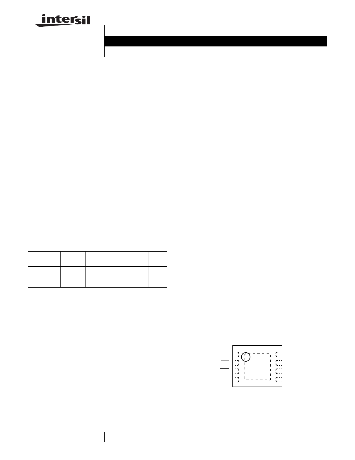
Pinout
(8 LD 2x3 DFN)
VIN
1
2
PPR
3
CHG
4
EN
ISL9204
TOP VIEW
BAT
8
7
IREF
6
IMIN
5
GND
1
CAUTION: These devices are sensitive to electrostatic discharge; follow proper IC Handling Procedures.
1-888-INTERSIL or 1-888-468-3774
| Intersil (and design) is a registered trademark of Intersil Americas Inc.
All other trademarks mentioned are the property of their respective owners.
Copyright © Intersil Americas Inc. 2005. All Rights Reserved
Page 2
ISL9204
Absolute Maximum Ratings (Reference to GND) Thermal Information
VIN. . . . . . . . . . . . . . . . . . . . . . . . . . . . . . . . . . . . . . . . -0.3V to 30V
IMIN, IREF, BAT, CHG, EN, PPR. . . . . . . . . . . . . . . . . . . . . . . . . -0.3V to 7V
Recommended Operating Conditions
Ambient Temperature Range. . . . . . . . . . . . . . . . . . . .-40°C to 85°C
Maximum Supply Voltage (VIN Pin). . . . . . . . . . . . . . . . . . . . . . 28V
Operating Supply Voltage (VIN Pin). . . . . . . . . . . . . . . . 4.3V to 10V
Programmed Charge Current . . . . . . . . . . . . . . . . . 50mA to 350mA
CAUTION: Stresses above those listed in “Absolute Maximum Ratings” may cause permanent damage to the device. This is a stress only rating and operation of the
device at these or any other conditions above those indicated in the operational sections of this specification is not implied.
NOTES:
is measured in free air with the component mounted on a high effective thermal conductivity test board with “direct attach” features. See
1. θ
JA
Tech Brief TB379.
2. For theta θ
the "case temp." location is the center of the exposed metal pad on the package underside.
JC
Electrical Specifications Typical Values Are Tested at VIN = 5V and the Ambient Temperature at 25°C. All Maximum and Minimum
Values Are Guaranteed Under the Recommended Operating Supply Voltage Range and Ambient Temperature
Range, Unless Otherwise Noted.
PARAMETER SYMBOL TEST CONDITIONS MIN TYP MAX UNITS
POWER-ON RESET
Rising POR Threshold V
Falling POR Threshold V
VIN-BAT OFFSET VOLTAGE
Rising Edge V
Falling Edge V
OVER VOLTAGE PROTECTION
Over Voltage Protection Threshold V
OVP Threshold Hysteresis 200 400 500 mV
STANDBY CURRENT
BAT Pin Sink Current I
VIN Pin Supply Current I
VIN Pin Supply Current I
VOLTAGE REGULATION
Output Voltage V
PMOS On Resistance r
CHARGE CURRENT (Note 5)
IREF Pin Output Voltage I
Constant Charge Current I
Trickle Charge Current I
End-of-Charge Current I
EOC Rising Threshold R
PRECONDITIONING CHARGE THRESHOLD
Preconditioning Charge Threshold
Voltage
Preconditioning Voltage Hysteresis V
POR
POR
OVP
STANDBY
VIN
VIN
DS(ON)VBAT
IREF
CHG
TRK
MIN
V
MINHYS
V
output.
OS
V
output (Note 3)
OS
Use PPR to indicate the comparator output (Note 4)
Charger disabled or the input is floating - - 1.0 µA
Charger disabled - 300 400 µA
Charger enabled - 500 700 µA
4.3V < V
CH
Charge current = 20mA
V
R
R
R
MIN
= 3.0V, use PPR to indicate the comparator
BAT
= 4.0V, use CHG pin to indicate the comparator
BAT
< 10V
IN
= 3.8V, charge current = 0.3A - 0.6 - Ω
= 3.8V 1.165 1.210 1.245 V
BAT
= 29.4kΩ, V
IREF
= 29.4kΩ, V
IREF
= 137kΩ 20 30 40 mA
IMIN
= 29.4kΩ 90 110 130 mA
IREF
Thermal Resistance (Typical, Notes 1, 2) θ
(°C/W) θJC (°C/W)
JA
DFN Package. . . . . . . . . . . . . . . . . . . . 59 4.5
Maximum Junction Temperature (Plastic Package) . . . . . . . . 150°C
Maximum Storage Temperature Range. . . . . . . . . . .-65°C to 150°C
Maximum Lead Temperature (Soldering 10s) . . . . . . . . . . . . . 300°C
(SOIC, PLCC, etc. Lead Tips Only)
3.3 3.9 4.3 V
3.1 3.6 4.15 V
- 90 150 mV
10 50 - mV
10 10.5 13 V
4.158 4.20 4.242 V
= 2.8V - 4.0V 135 150 165 mA
BAT
= 2.4V 18 25 32 mA
BAT
2.7 2.8 2.9 V
40 100 150 mV
2
FN9207.0
October 4, 2005
Page 3
ISL9204
Electrical Specifications Typical Values Are Tested at VIN = 5V and the Ambient Temperature at 25°C. All Maximum and Minimum
Values Are Guaranteed Under the Recommended Operating Supply Voltage Range and Ambient Temperature
Range, Unless Otherwise Noted. (Continued)
PARAMETER SYMBOL TEST CONDITIONS MIN TYP MAX UNITS
INTERNAL TEMPERATURE MONITORING
Charge Current Foldback Threshold
(Note 6)
LOGIC INPUT AND OUTPUTS
EN Pin Logic Input High 1.3 - - V
EN Pin Logic Input Low --0.5V
EN Pin Internal Pull Down
Resistance
CHG Sink Current When LOW Pin Voltage = 1V 10 20 - mA
CHG Leakage Current When HIGH V
PPR Sink Current When LOW Pin Voltage = 1V 10 20 - mA
PPR Leakage Current When HIGH V
NOTES:
3. The 4.0V V
is selected so that the CHG output can be used as the indication for the offset comparator output indication. If the V
BAT
than the POR threshold, no output pin can be used for indication.
4. For junction temperature from -40°C to120°C.
5. The charge current can be affected by the thermal foldback function if the IC under the test setup cannot dissipate the heat.
6. Guaranteed by characterization or correlation to other test.
T
FOLD
100 115 130 °C
100 200 400 kΩ
= 6.5V - - 1 µA
CHG
= 6.5V - - 1 µA
PPR
BAT
is lower
Typical Characteristics
4.5
4.3
4.1
3.9
3.7
CONSTANT
3.5
CURRENT
3.3
3.1
BAT VOLTAGE (V)
2.9
2.7
2.5
0 1K2K3K4K5K6K
CONSTANT
VOLTAGE
TIME (S)
0.20
0.18
0.16
0.14
0.12
0.10
0.08
0.06
0.04
0.02
0.00
Ichg (A)
FIGURE 1. COMPLETE CHARGE CYCLE (130mAh BATTERY) FIGURE 2. CONSTANT VOLTAGE vs CHARGE CURRENT
4.26
4.24
4.22
4.20
(V)
4.18
BAT
V
4.16
4.14
4.12
4.10
0 50 100 150 200 250 300 350
VIN = 5V
= 25°C
T
A
= 12.8K
R
IREF
(mA)
I
BAT
3
FN9207.0
October 4, 2005
Page 4

Typical Characteristics (Continued)
ISL9204
160.0
152.5
145.0
137.5
130.0
122.5
115.0
CHARGE CURRENT (mA)
107.5
100.0
456789101112
TA = 25°C
= 29.4K
R
IREF
= 3V
V
BAT
VIN (V)
FIGURE 3. CHARGE CURRENT vs VIN
240
210
VIN = 5V
180
150
120
90
60
CHARGE CURRENT (mA)
30
0
= 25°C
T
A
012345
V
BAT
(V)
R
IREF
19.5K
29.4K
= 59K
FIGURE 5. CHARGE CURRENT vs V
BAT
1.6
1.4
R
= 59K
IREF
1.2
1.0
0.8
VICDL (V)
0.6
0.4
0.2
0.0
0 50 100 150 200 250 300
29.4K 19.5K
VIN = 5V
= 25°C
T
A
= 3.9V
V
BAT
CHARGE CURRENT (mA)
FIGURE 4. VICDL vs CHARGE CURRENT
4.4
4.2
4.0
(V)
3.8
BAT
V
3.6
3.4
3.2
3.0
34567891011
FIGURE 6. V
VIN = 5V
T
I
VIN (V)
BAT
= 25°C
A
= 15mA
BAT
vs VIN
152
148
144
140
136
132
128
CHARGE CURRENT (mA)
124
120
-20-40 0 20 40 60 80 100 120
VIN = 5V
VB = 3.9V
= 29.4K
R
IREF
TEMPERATURE (°C)
FIGURE 7. CHARGE CURRENT vs TEMPERATURE
4
4.25
4.24
4.23
4.22
4.21
(V)
4.20
BAT
V
4.19
4.18
4.17
4.16
4.15
VIN = 5V
= 15mA
I
BAT
-20-40 0 20 40 60 80 100 120
TEMPERATURE (°C)
FIGURE 8. V
vs TEMPERATURE
BAT
FN9207.0
October 4, 2005
Page 5

ISL9204
Pin Descriptions
VIN - Power input. The absolute maximum input voltage is
28V. A 0.47µF or larger value X5R ceramic capacitor is
recommended to be placed very close to the input pin for
decoupling purpose. Additional capacitance may be required
to provide a stable input voltage.
PPR - Open-drain power presence indication. The opendrain MOSFET turns on when the input voltage is above the
POR threshold but below the OVP threshold and off
otherwise. This pin is capable to sink 10mA (minimum)
current to drive a LED. The maximum voltage rating for this
pin is 7V. This pin is independent on the EN-pin input.
CHG - Open-drain charge indication pin. This pin outputs a
logic LOW when a charge cycle starts and turns to HIGH
when the end-of-charge (EOC) condition is qualified. This
pin is capable to sink 10mA min. current to drive an LED.
When the charger is disabled, the CHG outputs high
impedance.
EN - Enable input. This is a logic input pin to disable or
enable the charger. Drive to HIGH to disable the charger.
When this pin is driven to LOW or left floating, the charger is
enabled. This pin has an internal 200kΩ pull-down resistor.
GND - System ground.
IMIN - End-of-charge (EOC) current program pin. Connect a
resistor between this pin and the GND pin to set the EOC
current. The EOC current IMIN can be programmed by the
following equation:
I
MIN
Where R
R
IMIN
is in kΩ. The programmable range covers 5%
IMIN
mA()=
4180
----------------
(or 10mA, whichever is higher) to 50% of IREF. When
programmed to less than 5% or 10mA, the stability is not
guaranteed.
IREF - Charge-current program and monitoring pin. Connect
a resistor between this pin and the GND pin to set the
charge current limit determined by the following equation:
I
REF
Where R
R
IREF
is in kΩ. The IREF pin voltage also monitors
IREF
mA()=
4400
-----------------
the actual charge current during the entire charge cycle,
including the trickle, constant-current, and constant-voltage
phases. When disabled, VIREF = 0V.
BAT - Charger output pin. Connect this pin to the battery. A
1µF or larger X5R ceramic capacitor is recommended for
decoupling and stability purposes. When the EN pin is pulled
to logic HIGH, the BAT output is disabled.
EPAD - Exposed pad. Connect as much as possible copper
to this pad either on the component layer or other layers
through thermal vias to enhance the thermal performance.
Typical Application
TO INPUT
C
1
ON
FIGURE 9. TYPICAL APPLICATION CIRCUIT INTERFACING TO INDICATION LEDS
OFF
VIN
EN
ISL9204
BAT
IREF
IMIN
CHG
PPR
GND
R
R
IREF
IMIN
TO BATTERY
1
D2
1
R2
C2
R
D
5
FN9207.0
October 4, 2005
Page 6

ISL9204
TABLE 1. COMPONENT DESCRIPTION FOR FIGURE 9
PART DESCRIPTION
R
D
R
R
C
C
IREF
IMIN
, R
1
, D
1
1
2
2
2
1µF X5R ceramic cap
1µF X5R ceramic cap
29.4kΩ, 1%, for 150mA charge current
137kΩ, 1%, for 30mA EOC current
300Ω, 5%
LEDs for indication
TO INPUT
VIN
C
1
OFF
EN
ON
ISL9204
TABLE 2. COMPONENT DESCRIPTION FOR FIGURE 10
PART DESCRIPTION
BAT
IREF
IMIN
CHG
R
R
R
C
C
IREF
IMIN
, R
1
1
2
R
R
2
IREF
IMIN
R1 R2
1µF X5R ceramic cap
1µF X5R ceramic cap
29.4kΩ, 1%, for 150mA charge current
137kΩ, 1%, for 30mA EOC current
100kΩ, 5%
TO BATTERY
C
2
VCC
VIN
PPR
EN
GND
GND
PPR
TO MCU
FIGURE 10. TYPICAL APPLICATION CIRCUIT WITH THE INDICATION SIGNALS INTERFACING TO A MCU
POR
PRE
REG
200kΩ
V
REF
VCC
VOS
BAT
CHARGE
CONTROL
EN
VCC
V
REF
DIE
TEMP
115°C
BAT
CHG
IMIN IREF
FIGURE 11. BLOCK DIAGRAM
6
FN9207.0
October 4, 2005
Page 7

ISL9204
TRICKLE CC CV
4.2V
I
REF
CHARGE
VOLTAGE
3.0V
17% I
REF
CHG
FIGURE 12. TYPICAL CHARGE PROFILE
Description
The ISL9204 charges a Li-ion battery with a constant current
(CC) or a constant voltage (CV). The constant current I
is set with the external resistor R
(see Figure 9) and the
IREF
constant voltage is fixed at 4.2V. If the battery voltage is
below a typical 2.8V trickle-charge threshold, the ISL9204
charges the battery with a trickle current until the battery
voltage rises above the trickle charge threshold. When the
battery voltage reaches 4.2V, the charger enters a CV mode
and regulates the battery voltage at 4.2V to fully charge the
battery without the risk of over charge. Upon reaching an
end-of-charge (EOC) current, the charger indicates the
charge completion with the CHG pin, but the charger
continues to output the 4.2V voltage. Figure 12 shows the
typical charge profile and the EOC/reset event.
The EOC current level I
external resistor R
IMIN
is programmable with the
MIN
(see Figure 9). The CHG signal turns
to LOW when the trickle charge starts and rises to HIGH at
the EOC. After the EOC is reached, the charge current has
to rise to typically 73% I
for the CHG signal to turn on
REF
again, as shown in Figure 12. The current surge after EOC
can be caused by a load connected to the battery.
A thermal foldback function reduces the charge current
anytime when the die temperature reaches typically 115°C.
This function guarantees safe operation when the printedcircuit board (PCB) is not capable of dissipating the heat
generated by the linear charger. The ISL9204 accepts an
input voltage up to 28V but disables charging when the input
voltage exceeds the OVP threshold, minimum 10V, to
protect against unqualified or faulty AC adapters.
PPR Indication
The PPR pin is an open-drain output to indicate the
presence of the AC adapter. Whenever the input voltage is
REF
CHARGE
CURRENT
I
MIN
CHG
INDICATION
73% I
TIME
REF
higher than the POR threshold, the PPR pin turns on the
internal open-drain MOSFET to indicate a logic LOW signal,
independent on the EN-pin input. When the internal opendrain FET is turned off, the PPR pin should leak less than
1µA current. When turned on, the PPR pin should be able to
sink at least 10mA current under all operating conditions.
The PPR pin can be used to drive an LED (see Figure 9) or
to interface with a microprocessor.
Power-Good Range
The power-good range is defined by the following three
conditions:
1. VIN > VPOR
2. VIN - VBAT > VOS
3. VIN < VOVP
where the VOS is the offset voltage for the input and output
voltage comparator, discussed shortly, and the VOVP is the
overvoltage protection threshold given in the Electrical
Specification. All V
, VOS, and V
POR
have hysteresis, as
OVP
given in the Electrical Specification table. The charger will
not charge the battery if the input voltage is not in the
power-good range.
Input and Output Comparator
The charger will not be enabled unless the input voltage is
higher than the battery voltage by an offset voltage VOS.
The purpose of this comparator is to ensure that the charger
is turned off when the input power is removed from the
charger. Without this comparator, it is possible that the
charger will fail to power down when the input is removed
and the current can leak through the PFET pass element to
continue biasing the POR and the Pre-Regulator blocks
shown in the Block Diagram.
7
FN9207.0
October 4, 2005
Page 8

ISL9204
CHG Indication
The CHG is an open-drain output capable to at least 10mA
current when the charger starts to charge and turns off when
the EOC current is reached. The CHG signal is interfaced
either with a micro-processor GPIO or an LED for indication.
EN Input
EN is an active-low logic input to enable the charger. Drive
the EN pin to LOW or leave it floating to enable the charger.
This pin has a 200kΩ internal pulldown resistor so when left
floating, the input is equivalent to logic LOW. Drive this pin to
HIGH to disable the charger. The threshold for HIGH is given
in the ES (Electrical Specification) table.
IREF Pin
The IREF pin has the two functions as described in the Pin
Description section. When setting the fast charge current,
the charge current is guaranteed to have 10% accuracy with
the charge current set at 150mA. When monitoring the
charge current, the accuracy of the IREF pin voltage vs. the
actual charge current has the same accuracy as the gain
from the IREF pin current to the actual charge current. The
accuracy is 10% at 150mA and is expected to drop to 30% of
the actual current (not the set constant charge current) when
the current drops to 50mA.
Operation Without the Battery
The ISL9204 relies on a battery for stability and is not
guaranteed to be stable if the battery is not connected. With
a battery, the charger will be stable with an output ceramic
decoupling capacitor in the range of 1µF to 200µF. The
maximum load current is limited by the dropout voltage or
the thermal foldback.
Dropout Voltage
The constant current may not be maintained due to the
r
resistance of the pass FET is 1.2Ω the maximum operating
temperature, thus if tested with 350mA current and 4.2V
battery voltage, constant current could not be maintained
when the input voltage is below 4.62V.
limit at a low input voltage. The worst case on
DS(ON)
Thermal Foldback
The thermal foldback function starts to reduce the charge
current when the internal temperature reaches a typical
value of 115°C.
Applications Information
Input Capacitor Selection
The input capacitor is required to suppress the power supply
transient response during transitions. Mainly this capacitor is
selected to avoid oscillation during the start up when the
input supply is passing the POR threshold and the VIN-BAT
comparator offset voltage. When the battery voltage is above
the POR threshold, the VIN-VBAT offset voltage dominates
the hysteresis value. Typically, a 1µF X5R ceramic capacitor
should be sufficient to suppress the power supply noise.
Output Capacitor Selection
The criteria for selecting the output capacitor is to maintain
the stability of the charger as well as to bypass any transient
load current. The minimum capacitance is a 1µF X5R
ceramic capacitor. The actual capacitance connected to the
output is dependent on the actual application requirement.
Charge Current Limit
The actual charge current in the CC mode is limited by
several factors in addition to the set I
three limits for the charge current in the CC mode. The
charge current is limited by the on resistance of the pass
element (power P-channel MOSFET) if the input and the
output voltage are too close to each other. The solid curve
shows a typical case when the battery voltage is 4.0V and
the charge current is set to 350mA. The non-linearity on the
R
-limited region is due to the increased resistance at
ON
higher die temperature. If the battery voltage increases to
higher than 4.0V, the entire curve moves towards right side.
As the input voltage increases, the charge current may be
reduced due to the thermal foldback function. The limit
caused by the thermal limit is dependent on the thermal
impedance. As the thermal impedance increases, the
thermal-limited curve moves towards left, as shown in
Figure 13.
Layout Guidance
The ISL9204 uses a thermally-enhanced DFN package that
has an exposed thermal pad at the bottom side of the
package. The layout should connect as much as possible to
copper on the exposed pad. Typically the component layer is
more effective in dissipating heat. The thermal impedance
can be further reduced by using other layers of copper
connecting to the exposed pad through a thermal via array.
Each thermal via is recommended to have 0.3mm diameter
and 1mm distance from other thermal vias.
. Figure 13 shows
REF
8
FN9207.0
October 4, 2005
Page 9

Input Power Sources
The input power source is typically a well-regulated wall
cube with 1-meter length wire or a USB port. The input
voltage ranges from 4.3V to 10V. The ISL9204 can withstand
up to 28V on the input without damaging the IC. If the input
voltage is higher than the OVP threshold, the charger stops
charging.
ISL9204
350
CHARGE CURRENT (mA)
R
ON
LIMITED
INCREASES
4.5 5.0 5.5
INPUT VOLTAGE (V)
INCREASES
V
BAT
R
IREF
THERMAL
LIMITED
θ
OR T
JA
INCREASES
A
\\
FIGURE 13. CHARGE CURRENT LIMITS IN CONSTANT
CURRENT MODE
10 4.0
9
FN9207.0
October 4, 2005
Page 10

Dual Flat No-Lead Plastic Package (DFN)
ISL9204
(DATUM A)
NX (b)
5
INDEX
AREA
SEATING
(DATUM B)
6
INDEX
AREA
NX L
8
A
6
C
PLANE
(A1)
D
TOP VIEW
SIDE VIEW
D2
D2/2
12
N
N-1
e
(Nd-1)Xe
REF.
BOTTOM VIEW
2X
A3
NX b
L8.2x3
ABC0.15
2X
0.15
CB
E
0.10
//
A
87
NX k
E2
E2/2
5
0.10
C
L
0.08
L
C
C
BAMC
8 LEAD DUAL FLAT NO-LEAD PLASTIC PACKAGE
MILLIMETERS
SYMBOL
NOTESMIN NOMINAL MAX
A 0.80 0.90 1.00 -
A1 - - 0.05 -
A3 0.20 REF -
b 0.20 0.25 0.32 5,8
D 2.00 BSC -
D2 1.50 1.65 1.75 7,8
E 3.00 BSC -
E2 1.65 1.80 1.90 7,8
e 0.50 BSC -
k0.20 - - -
L 0.30 0.40 0.50 8
N 8 2
Nd 4 3
Rev. 0 6/04
NOTES:
1. Dimensioning and tolerancing conform to ASME Y14.5-1994.
2. N is the number of terminals.
3. Nd refers to the number of terminals on D.
4. All dimensions are in millimeters. Angles are in degrees.
5. Dimension b applies to the metallized terminal and is measured
between 0.25mm and 0.30mm from the terminal tip.
6. The configuration of the pin #1 identifier is optional, but must be
located within the zone indicated. The pin #1 identifier may be
either a mold or mark feature.
7. Dimensions D2 and E2 are for the exposed pads which provide
improved electrical and thermal performance.
8. Nominal dimensions are provided to assist with PCB Land
Pattern Design efforts, see Intersil Technical Brief TB389.
SECTION "C-C"
FOR EVEN TERMINAL/SIDE
CC
e
TERMINAL TIP
All Intersil U.S. products are manufactured, assembled and tested utilizing ISO9000 quality systems.
Intersil Corporation’s quality certifications can be viewed at www.intersil.com/design/quality
Intersil products are sold by description only. Intersil Corporation reserves the right to make changes in circuit design, software and/or specifications at any time without
notice. Accordingly, the reader is cautioned to verify that data sheets are current before placing orders. Information furnished by Intersil is believed to be accurate and
reliable. However, no responsibility is assumed by Intersil or its subsidiaries for its use; nor for any infringements of patents or other rights of third parties which may result
from its use. No license is granted by implication or otherwise under any patent or patent rights of Intersil or its subsidiaries.
For information regarding Intersil Corporation and its products, see www.intersil.com
10
FN9207.0
October 4, 2005
 Loading...