

Page 1
®
ISL9200
Data Sheet October 4, 2005
Charging System Safety Circuit
The ISL9200 is an integrated circuit (IC) optimized to provide
a Li-ion battery redundant safety protection from failures of a
charging system. The IC monitors the input voltage, the
battery voltage, and the charge current. When any of the
three parameters exceeds its limit, the IC turns off an internal
P-channel MOSFET to remove the power from the charging
system. In addition to the above protected parameters, the
IC also monitors its own internal temperature and turns off
the P-channel MOSFET when the die temperature exceeds
140°C. Together with the battery charger IC and the
protection module in a battery pack, the charging system
using the ISL9200 has triple-level protection and is two-fault
tolerant.
The IC is designed to turn on the internal PFET slowly to
avoid inrush current at power-up but will turn off the PFET
quickly when input overvoltage is detected, in order to
remove the power before any damage occurs. The ISL9200
has a logic warning output to indicate the fault and an enable
input to allow the system to remove the input power.
Ordering Information
PAR T
PAR T #
ISL9200IRZ*
(Note)
ISL9200EVAL1 ISL9200 Evaluation Board
*Add “-T” suffix for tape and reel.
NOTE: Intersil Pb-free plus anneal products employ special Pb-free
material sets; molding compounds/die attach materials and 100%
matte tin plate termination finish, which are RoHS compliant and
compatible with both SnPb and Pb-free soldering operations. Intersil
Pb-free products are MSL classified at Pb-free peak reflow
temperatures that meet or exceed the Pb-free requirements of
IPC/JEDEC J STD-020.
MARKING
00Z
TEMP.
RANGE (°C) PACKAGE
-40 to 85 12 Ld 4x3 DFN
(Pb-free)
PKG.
DWG. #
L12.4x3
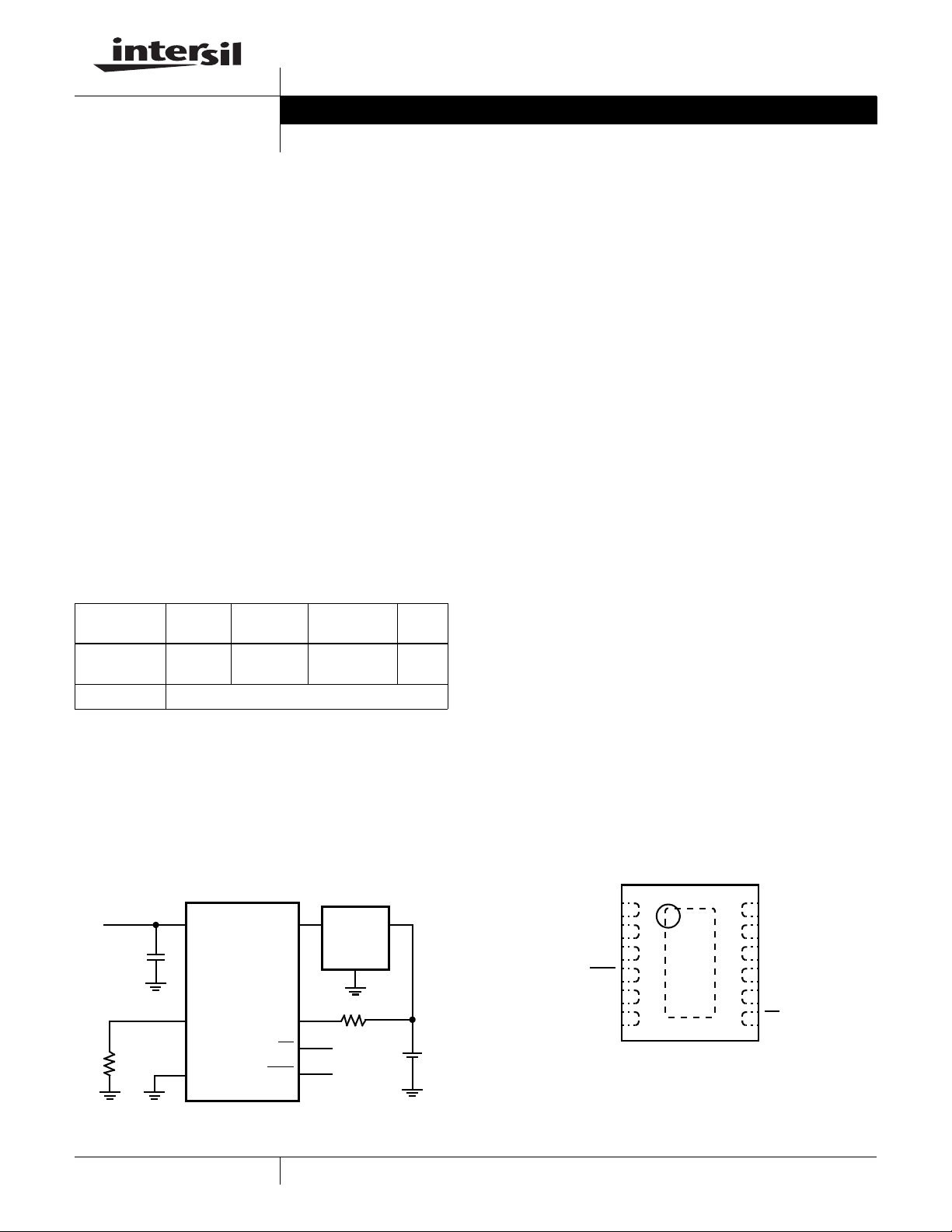
Typical Application Circuit
FN9241.0
Features
• Fully Integrated Protection Circuit for Three Protection
Var iable s
- User Programmable Overcurrent Protection Threshold
- Input Overvoltage Protection in Less Than 1µs
- Battery Overvoltage Protection
• High Immunity of False Triggering Under Transients
• High Accuracy Protection Thresholds
• Warning Output to Indicate the Occurrence of Faults
• Enable Input
• Thermal Enhanced DFN Package
• Pb-Free Plus Anneal Available (RoHS Compliant)
Applications
• Cell Phones
• Digital Still Cameras
• PDAs and Smart Phones
• Portable Instruments
• Desktop Chargers
Related Literature
• Technical Brief TB363 “Guidelines for Handling and
Processing Moisture Sensitive Surface Mount Devices
(SMDs)”
• Technical Brief TB379 “Thermal Characterization of
Packaged Semiconductor Devices”
• Technical Brief TB389 “PCB Land Pattern Design and
Surface Mount Guidelines for QFN Packages”
Pinout
ISL9200 (4x3 DFN)
TOP VIEW
INPUT
R
C
ILIM
VIN
VIN
1
ISL9200
ILIM
GND
OUT
VB
EN
WRN
1
ISL6292
BATTERY
CHARGER
R
VB
BATTERY
PAC K
+
NOTE: EPAD must be electrically connected to the GND pin.
CAUTION: These devices are sensitive to electrostatic discharge; follow proper IC Handling Procedures.
1-888-INTERSIL or 1-888-468-3774
| Intersil (and design) is a registered trademark of Intersil Americas Inc.
All other trademarks mentioned are the property of their respective owners.
1
2
VIN
3
GND
4
WRN
NC
5
NC EN
6 7
Copyright © Intersil Americas Inc. 2005. All Rights Reserved.
EPAD
NC
12
11
OUT
10
OUT
9
ILIM
VB
8
Page 2
ISL9200
Absolute Maximum Ratings (Reference to GND) Thermal Information
Supply Voltage (VIN) . . . . . . . . . . . . . . . . . . . . . . . . . . . . -0.3 to 30V
Output and VB Pin (OUT, VB) (Note 1) . . . . . . . . . . . . . . . -0.3 to 7V
Other Pins (ILIM, WRN
, EN) . . . . . . . . . . . . . . . . . . . . . -0.3 to 5.5V
ESD Rating
Human Body Model (Per JESD22-A114-B) . . . . . . . . . . . . .3000V
Machine Model (Per EIA/JESD22 A115-A) . . . . . . . . . . . . . .200V
Recommended Operating Conditions
Ambient Temperature Range . . . . . . . . . . . . . . . . . . . . -40°C to 85°C
Supply Voltage, VIN. . . . . . . . . . . . . . . . . . . . . . . . . . . 4.3V to 6.5V
CAUTION: Stresses above those listed in “Absolute Maximum Ratings” may cause permanent damage to the device. This is a stress only rating and operation of the
device at these or any other conditions above those indicated in the operational sections of this specification is not implied.
NOTES:
1. The maximum voltage rating for the VB pin under continuous operating conditions is 5.5V. All other pins are allowed to operate continuously at
the absolute maximum ratings.
is measured in free air with the component mounted on a high effective thermal conductivity test board with “direct attach” features. See
2. θ
JA
Tech Brief TB379.
, “case temperature” location is at the center of the exposed metal pad on the package underside. See Tech Brief TB379.
3. θ
JC
Electrical Specifications Typical values are tested at VIN = 5V and 25°C Ambient Temperature, maximum and minimum values are
guaranteed over the recommended operating conditions, unless otherwise noted.
PARAMETER SYMBOL TEST CONDITIONS MIN TYP MAX UNITS
POWER-ON RESET
Rising VIN Threshold V
POR Hysteresis - 100 - mV
VIN Bias Current I
VIN Bias Current When disabled 30 60 100 µA
PROTECTIONS
Input Overvoltage Protection (OVP) V
Input OVP Hysteresis - 60 100 mV
Input OVP Falling Threshold 6.55 - - V
Input OVP Propagation Delay --1µs
Overcurrent Protection I
Overcurrent Protection Blanking Time BT
Battery Overvoltage Protection Threshold V
Battery OVP Threshold Hysteresis 75 - mV
Battery OVP Falling Threshold 4.225 - - V
Battery OVP Blanking Time BT
VB Pin Leakage Current V
Over Temperature Protection Rising Threshold 140 - °C
Over Temperature Protection Falling Threshold - 90 - °C
LOGIC
Input Logic HIGH 1.5 - - V
EN
EN Input Logic LOW --0.4V
EN Internal Pull Down Resistor 100 200 400 kΩ
WRN Output Logic Low Sink 5mA current - 0.35 0.8 V
WRN Output Logic High Leakage Current - - 1 µA
POWER MOSFET
On Resistance R
POR
VIN
OVP
OCP
OCP
BOVP
BOVP
DS(ON)
When enabled 0.75 0.9 1.05 mA
VVB = 3V, R
= 4.4V - 20 nA
VB
Measured at 500mA, 4.3V < V
Thermal Resistance (Notes 2, 3) θ
(°C/W) θJC (°C/W)
JA
4x3 DFN Package . . . . . . . . . . . . . . . . 41 3.5
Maximum Junction Temperature (Plastic Package) . . . . . . . . 150°C
Maximum Storage Temperature Range. . . . . . . . . . . -65°C to 150°C
Maximum Lead Temperature (Soldering 10s) . . . . . . . . . . . . . 300°C
2.4 2.58 2.7 V
6.65 6.8 7.0 V
= 25kΩ 0.93 1.0 1.07 A
ILIM
- 170 - µs
4.325 4.4 4.475 V
180 - µs
< 6.5V - 250 450 mΩ
IN
2
FN9241.0
October 4, 2005
Page 3
ISL9200
Pin Descriptions
VIN (Pins 1, 2)
The input power source. The VIN can withstand 30V input.
GND (Pin 3)
System ground reference.
WRN (Pin 4)
WRN is an open-drain logic output that turns LOW when any
protection event occurs.
NC (Pins 5, 6, 12)
No connection and must be left floating.
EN (Pin 7)
Enable input. Pull this pin to low or leave it floating to enable
the IC and force it to high to disable the IC.
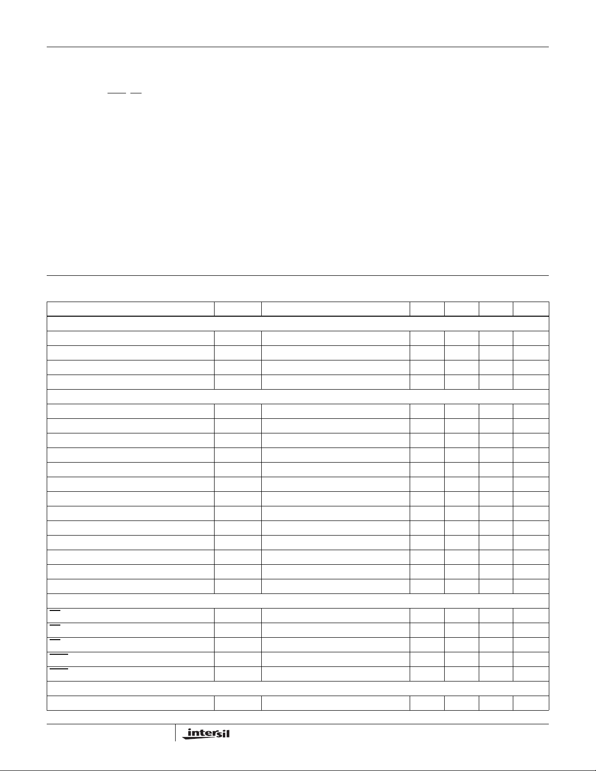
Typical Applications
INPUT
R
C
ILIM
1
VIN
ILIM
GND
ISL9200
OUT
VB
EN
WRN
ISL6292
BATTERY
CHARGER
R
VB
BATTERY
PACK
VB (Pin 8)
Battery voltage monitoring input. This pin is connected to the
battery pack positive terminal via an isolation resistor.
ILIM (Pin 9)
Overcurrent protection threshold setting pin. Connect a
resistor between this pin and GND to set the OCP threshold.
OUT (Pins 10, 11)
Output pin.
EPAD
The exposed pad at the bottom of the DFN package for
enhancing thermal performance. Must be electrically
connected to the GND pin.
PART DESCRIPTION
R
ILIM
R
VB
+
C1 1µF/16V X5R ceramic capacitor
25kΩ
200kΩ to 1MΩ
Block Diagram
INPUT
VIN
OUT
Q
1
Q
2 Q
POR
PRE-REG
WRN
1. 2V
REF
Q
CP1
4
R
1
R
2
GND
FET
DRIV ER
LOGIC
CP2
CP3
Q
5
R
5
EN
3
EA
0.8V
R
3
R
4
ILIM
VB
BUF
I SL6292
BATT ERY
CHARGE R
R
ILIM
R
VB
+
FIGURE 1. BLOCK DIAGRAM
3
FN9241.0
October 4, 2005
Page 4
ISL9200
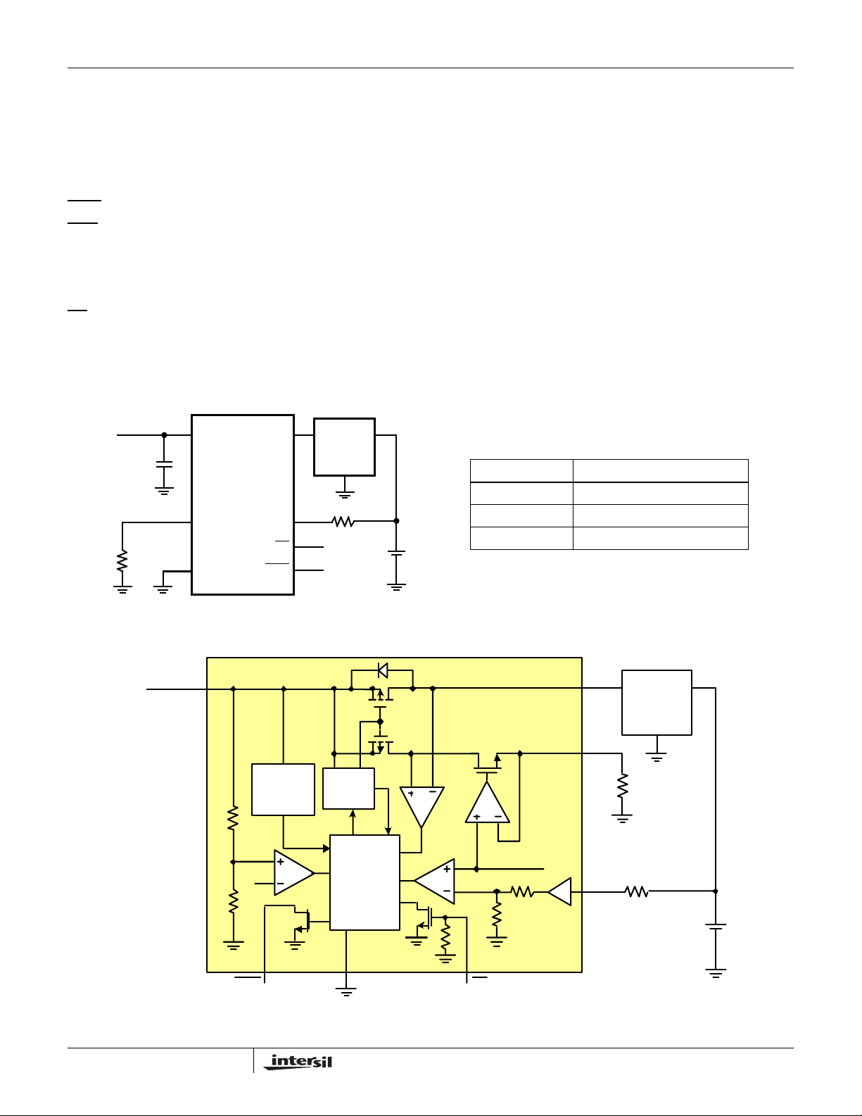
Typical Operating Performance The test conditions for the Typical Operating Performance are: V
R
= 25.5kΩ, RVB = 200kΩ, Unless Otherwise Noted.
ILIM
VIN (1V/div)
OUT (1V/div)
Load Current
(200mA/div)
Time: 5ms/div
FIGURE 2. CAPTURED WAVEFORMS FOR POWER-UP. THE
OUTPUT IS LOADED WITH A 10Ω RESISTOR
Time: 200ms/div
VIN (2V/div)
FIGURE 3. CAPTURED WAVEFORMS WHEN THE INPUT
WRN (5V/div)
VOLTAGE STEPS FROM 6.5V TO 10.5V
VIN (2V/div)
= 5V, TA = 25°C,
IN
VIN (2V/div)
OUT (2V/div)
Time: 2µs/div
OUT (2V/div)
WRN (5V/div)
FIGURE 4. CAPTURED WAVEFORMS WHEN THE INPUT
GRADUALLY RISES TO THE INPUT
OVERVOLTAGE THRESHOLD
VIN (2V/div)
ILIM (1V/div)
WRN (5V/div)
OUT (2V/div)
Time: 500µs/div
OUT (2V/div)
WRN (5V/div)
FIGURE 5. TRANSIENT WHEN THE INPUT VOLTAGE STEPS
FROM 7.5V TO 6.5V
Time: 20s/div
Time: 5ms/div
VIN (1V/div)
VB (1V/div)
OUT (1V/div)
WRN (5V/div)
FIGURE 6. TRANSIENT WAVEFORMS WHEN INPUT STEPS
FROM ZERO TO 9V
4
FIGURE 7. BATTERY OVERVOLTAGE PROTECTION. THE IC
IS LATCHED OFF AFTER 16 COUNTS OF
PROTECTION. VB VOLTAGE VARIES BETWEEN
4.3V TO 4.5V
FN9241.0
October 4, 2005
Page 5
ISL9200
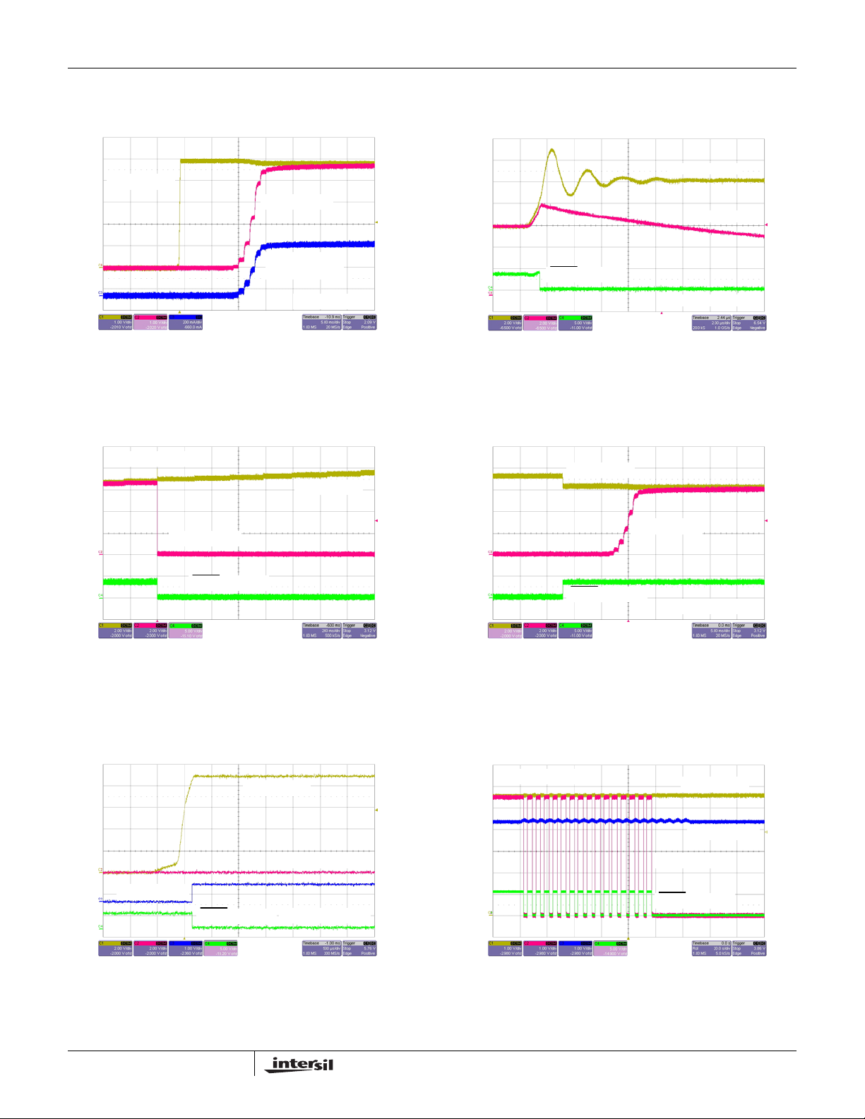
Typical Operating Performance The test conditions for the Typical Operating Performance are: V
R
= 25.5kΩ, RVB = 200kΩ, Unless Otherwise Noted. (Continued)
ILIM
Time: 200ms/div
VIN (1V/div)
OUT (1V/div)
Load Current
(500mA/div)
WRN (5V/div)
FIGURE 8. POWER-UP WAVEFORMS WHEN OUTPUT IS
SHORT-CIRCUITED
1200
1000
800
600
400
INPUT BIAS CURRENT (µA)
200
0
0 5 10 15 20 25 30 35
INPUT VOLTAGE (V)
ENABLED
DISABLED
FIGURE 10. INPUT BIAS CURRENT vs INPUT VOLTAGE
WHEN ENABLED AND DISABLED
Time: 10ms/div
Load Current
(500mA/div)
OUT (1V/div)
WRN (5V/div)
FIGURE 9. ZOOMED-IN VIEW OF FIGURE 8 (BLUE: LOAD
CURRENT; PINK: OUT PIN VOLTAGE)
1000
6.5V/ENABLED
900
800
700
600
500
400
CURRENT (µA)
300
200
100
0
-50 -20 10 40 70 100 130
5V/ENABLED
30V/ENABLED
30V/DISABLED
6.5V/DISABLED
5V/DISABLED
TEMPERATURE (°C)
FIGURE 11. INPUT BIAS CURRENT AT DIFFERENT INPUT
VOLTAGES WHEN ENABLED AND DISABLED
= 5V, TA = 25°C,
IN
VIN (1V/div)
4.3V/ENABLED
4.3V/DISABLED
2.6
2.58
2.56
2.54
(V)
POR
2.52
V
2.5
2.48
2.46
-50 -20 10 40 70 100 130
FIGURE 12. V
RISING THRESHOLD
FALLING THRESHOLD
TEMPERATURE (°C)
vs TEMPERATURE FIGURE 13. INPUT OVERVOLTAGE PROTECTION
POR
5
6.95
6.9
6.85
(V)
6.8
OVP
V
6.75
6.7
6.65
-50 -20 10 40 70 100 130
RISING THRESHOLD
FALLING THRESHOLD
TEMPERATURE (°C)
THRESHOLDS vs TEMPERATURE
FN9241.0
October 4, 2005
Page 6

ISL9200
Typical Operating Performance The test conditions for the Typical Operating Performance are: V
R
= 25.5kΩ, RVB = 200kΩ, Unless Otherwise Noted. (Continued)
ILIM
1050
CURRENT
1040
LIMIT = 1A
1030
1020
1010
(mA)
OCP
I
1000
990
980
970
960
5V
4.3V
-50 -20 10 40 70 100 130
3V
TEMPERATURE (°C)
6.5V
FIGURE 14. OVERCURRENT PROTECTION THRESHOLDS vs
TEMPERATURE AT VARIOUS INPUT VOLTAGES
515
510
505
500
495
(mA)
490
OCP
I
485
480
475
470
-50 -20 10 40 70 100 130
4.3V
6.5V
3V
5V
TEMPERATURE (°C)
FIGURE 16. OVERCURRENT PROTECTION THRESHOLDS vs
TEMPERATURE AT VARIOUS INPUT VOLTAGES
FIGURE 15. OVERCURRENT PROTECTION BLANKING TIME
FIGURE 17. BATTERY VOLTAGE OVP THRESHOLDS vs
200
195
190
185
180
(µs)
175
OCP
170
BT
165
160
155
150
-50 -20 10 40 70 100 130
TEMPERATURE (°C)
vs TEMPERATURE
4.42
4.41
4.4
4.39
4.38
(V)
4.37
BOVP
V
4.36
4.35
4.34
4.33
4.32
-50 -20 10 40 70 100 130
RISING THRESHOLDS FOR
4.5V, 5V AND 6.5V INPUT
FALLING THRESHOLDS FOR
4.5V, 5V AND 6.5V INPUT
TEMPERATURE (°C)
TEMPERATURE AT VARIOUS INPUT VOLTAGES
= 5V, TA = 25°C,
IN
200
195
190
185
180
(µs)
175
BOVP
170
BT
165
160
155
150
-50 -20 10 40 70 100 130
TEMPERATURE (°C)
3.0
TESTED AT 5V
2.5
2.0
1.5
1.0
0.5
VB PIN LEAKAGE CURRENT (nA)
0
-50 -20 10 40 70 100 130
TEMPERATURE (°C)
FIGURE 18. BATTERY OVP BLANKING TIME FIGURE 19. VB PIN LEAKAGE CURRENT vs TEMPERATURE
6
October 4, 2005
FN9241.0
Page 7

ISL9200
Typical Operating Performance The test conditions for the Typical Operating Performance are: V
R
= 25.5kΩ, RVB = 200kΩ, Unless Otherwise Noted. (Continued)
ILIM
2.0
1.8
1.6
1.4
1.2
1.0
0.8
0.6
EN THRESHOLD (V)
0.4
0.2
0
-50 -20 10 40 70 100 130
TEMPERATURE (°C)
250
240
230
220
210
200
190
180
170
160
EN PIN INTERNAL PULL-DOWN (kΩ)
150
-50 -20 10 40 70 100 130
TEMPERATURE (°C)
= 5V, TA = 25°C,
IN
FIGURE 20. EN INPUT THRESHOLD vs TEMPERATURE FIGURE 21. EN PIN INTERNAL PULL-DOWN RESISTANCE
0.5
0.4
3V
4.3V
0.3
(Ω)
DS(ON)
0.2
R
0.1
0
-50 -20 10 40 70 100 130
FIGURE 22. ON RESISTANCE vs TEMPERATURE AT DIFFERENT INPUT VOLTAGES
Theory of Operation
The ISL9200 is an integrated circuit (IC) optimized to provide
a redundant safety protection to a Li-ion battery from
charging system failures. The IC monitors the input voltage,
the battery voltage, and the charge current. When any of the
above three parameters exceeds its limit, the IC turns off an
internal P-channel MOSFET to remove the power from the
charging system. In addition to the above protected
parameters, the IC also monitors its own internal
temperature and turns off the P-channel MOSFET when the
temperature exceeds 140°C. Together with the battery
charger IC and the protection module in a battery pack, the
charging system has triple-level protection from overcharging the Li-ion battery and is two-fault tolerant. The
ISL9200 protects up to 30V input voltage.
5V
6.5V
TEMPERATURE (°C)
Power-Up
The ISL9200 has a power-on reset (POR) threshold of 2.6V
with a built-in hysteresis of 100mV. Before the input voltage
reaches the POR threshold, the internal power PFET is off.
Approximately 10ms after the input voltage exceeds the
POR threshold, the IC resets itself and begins the soft-start.
The 10ms delay allows any transients at the input during a
hot insertion of the power supply to settle down before the IC
starts to operate. The soft-start slowly turns on the power
PFET to reduce the inrush current as well as the input
voltage drop during the transition. The power-up behavior is
illustrated in Figure 2.
Input Overvoltage Protection (OVP)
The input voltage is monitored by the comparator CP1 in the
Block Diagram (Figure 1). CP1 has an accurate reference of
1.2V from the bandgap reference. The OVP threshold is set
by the resistive divider consisting of R1 and R2. The
7
FN9241.0
October 4, 2005
Page 8

ISL9200
protection threshold is set to 6.8V. When the input voltage
exceeds the threshold, the CP1 outputs a logic signal to turn
off the power PFET within 1µs (see Figure 3) to prevent the
high input voltage from damaging the electronics in the
handheld system. The hysteresis for the input OVP
threshold is given in the Electrical Specification. When the
input overvoltage condition is removed, the ISL9200 reenables the output by running through the soft-start, as
shown in Figure 5. Because of the 10ms second delay
before the soft-start, the output is never enabled if the input
rises above the OVP threshold quickly, as shown in Figure 6.
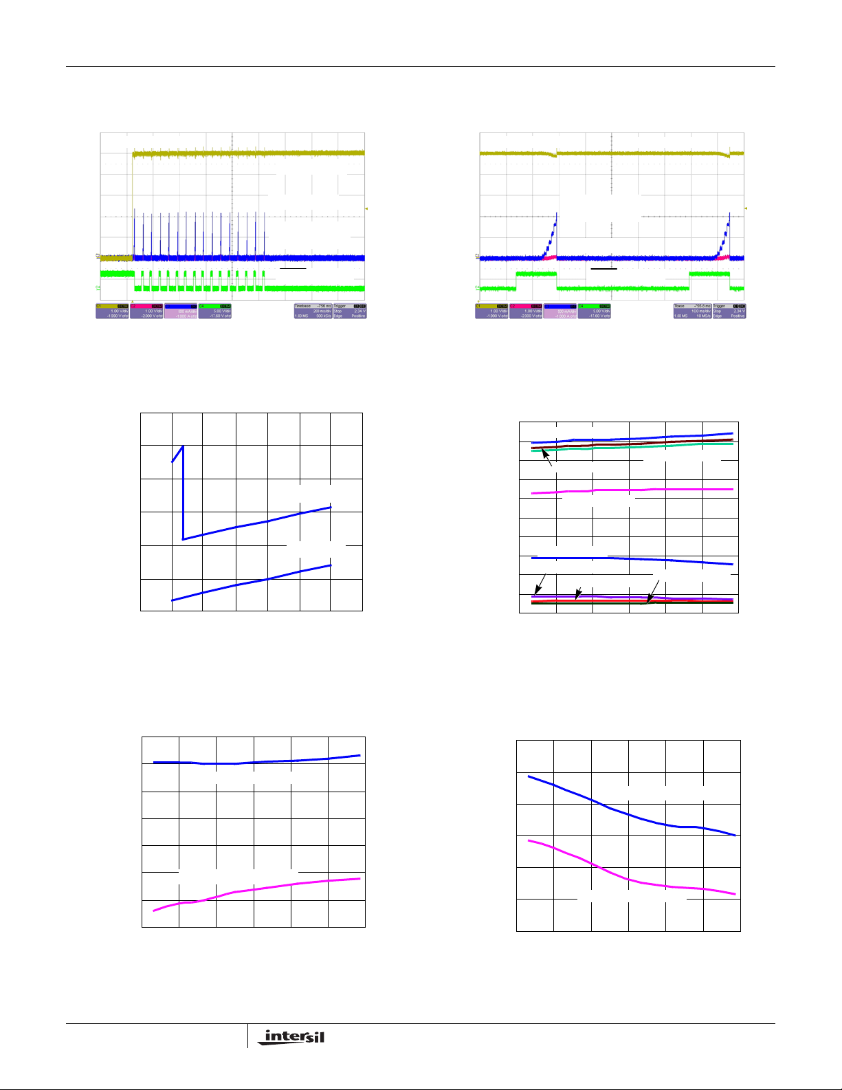
Battery Overvoltage Protection
The battery voltage OVP is realized with the VB pin. The
comparator CP3, as shown in Figure 1, monitors the VB pin
and issues an overvoltage signal when the battery voltage
exceeds the 4.4V battery OVP threshold. The threshold has
75mV built-in hysteresis. The comparator CP3 has a built-in
180µs blanking time to prevent any transient voltage from
triggering the OVP. If the OVP situation still exists after the
blanking time, the power PFET is turned off. The control
logic contains a 4-bit binary counter that if the battery
overvoltage event occurs 16 times, the power PFET is
turned off permanently, as shown in Figure 7. Recycling the
input power or toggling the enable (EN
) input will reset the
counter and restart the ISL9200.
The resistor between the VB pin and the battery, R
VB
, as
shown in the Typical Applications circuit, is an important
component. This resistor provides a current limit in case the
VB pin is shorted to the input voltage under a failure mode.
The VB pin leakage current under normal operation is
negligible to allow a resistance of 200kΩ to 1MΩ be used.
Overcurrent Protection (OCP)
The current in the power PFET is limited to prevent charging
the battery with an excessive current. The current is sensed
using the voltage drop across the power FET after the FET is
turned on. The reference of the OCP is generated using a
sensing FET Q2, as shown in Figure 1. The current in the
sensing FET is forced to the value programmed by the ILIM
pin. The size of the power FET Q1 is 31,250 times the size
of the sensing FET. Therefore, when the current in the power
FET is 31,250 times the current in the sensing FET, the drain
voltage of the power FET falls below that of the sensing FET.
The comparator CP2 then outputs a signal to turn off the
power FET.
The OCP threshold can be calculated using the following
equation:
0.8V
---------------
I
LIM
R
31250
ILIM
where the 0.8V is the regulated voltage at the ILIM pin. The
OCP comparator CP2 has a built-in 170µs delay to prevent
false triggering by transient signals. The OCP function also
has a 4-bit binary counter that accumulates during an OCP
25000
----------------=⋅=
R
ILIM
event. When the total count reaches 16, the power PFET is
turned off permanently unless the input power is recycled or
the enable pin is toggled. Figure 8 and Figure 9 illustrate the
waveforms during the power-up when the output is shortcircuited to ground.
Internal Over Temperature Protection
The ISL9200 monitors its own internal temperature to
prevent thermal failures. When the internal temperature
reaches 140°C, the IC turns off the P-channel power
MOSFET. The IC does not resume operation until the
internal temperature drops below 90°C.
External Enable Control
The ISL9200 offers an enable (EN) input. When the EN pin
is pulled to logic HIGH, the protection IC is shut down. The
internal control circuit as well as the power PFET are turned
off. Both 4-bit binary counters for the battery OVP and the
OCP are reset to zero when the IC is re-enabled. The EN
has an internal 200kΩ pull-down resistor. Leaving the EN
pin
pin
floating or driving it to below 0.4V enables the IC.
Warning Indication Output
The WRN pin is an open-drain output that indicates a LOW
signal when any of the three protection events happens. This
allows the microprocessor to give an indication to the user to
further enhance the safety of the charging system.
Applications Information
The ISL9200 is designed to meet the “Lithium-Safe” criteria
when operating together with the ISL6292 family Li-ion
battery chargers. The “Lithium-Safe” criteria requires the
charger output to fall within the green region shown in
Figure 23 under normal operating conditions and NOT to fall
in the red region when there is a single fault in the charging
system. Taking into account the safety circuit in a Li-ion
battery pack, the charging system is allowed to have two
faults without creating hazardous conditions for the battery
cell. The output of any ISL6292 family chargers, such as the
ISL6292C, has a typical I-V curve shown with the blue lines
under normal operation, which is within the green region.
The function of the ISL9200 is to add an redundant
protection layer such that, under any single fault condition,
the charging system output does not exceed the I-V limits
shown with the red lines. As a result, the charging system
adopting the ISL9200 and the ISL6292C chip set can easily
pass the “Lithium-Safe” criteria test procedures.
The ISL9200 is a simple device that requires only three
external components, in addition to the ISL6292 charger
circuit, to meet the “Lithium-Safe” criteria, as shown in the
Typical Application Circuit. The selection of the current limit
resistor R
is given in the Overcurrent Protection section.
ILIM
8
FN9241.0
October 4, 2005
Page 9

ISL9200
RVB Selection
The RVB prevents a large current from the VB pin to the
battery terminal, in case the ISL9200 fails. The
recommended value should be between 200kΩ to 1MΩ.
With 200kΩ resistance, the worst case current flowing from
the VB pin to the charger output is,
(30V - 4.2V)/200kΩ = 130µA,
assuming the VB pin voltage is 30V under a failure mode
and the battery voltage is 4.2V. Such a small current can be
easily absorbed by the bias current of other components in
the handheld system. Increasing the R
worst case current, but at the same time increases the error
for the 4.4V battery OVP threshold.
The error of the battery OVP threshold is the original
accuracy at the VB pin given in the Electrical Specification
plus the voltage built across the R
current. The VB pin leakage current is less than 20nA, as
given in the Electrical Specification. With the 200kΩ resistor,
the worst-case additional error is 4mV and with a 1MΩ
resistor, the worst-case additional error is 20mV.
1000
ISL 9200
LIMITS
ISL 6292C
LIMITS
CHARG E CURRE NT (mA)
value reduces the
VB
by the VB pin leakage
VB
ISL9200 MCU
Q
4
Q
5
FIGURE 24. DIGITAL SIGNAL INTERFACE BETWEEN ISL9200
AND MCU
WRN
EN
R
5
VIO
R
PU
R
WRN
R
EN
Capacitor Selection
The input capacitor (C1 in the Typical Application Circuit) is
for decoupling. Higher value reduces the voltage drop or the
over shoot during transients.
Two scenarios can cause the input voltage over shoot. The
first one is when the AC adapter is inserted live (hot
insertion) and the second one is when the current in the
power PFET of the ISL9200 has a step-down change. Figure
25 shows an equivalent circuit for the ISL9200 input. The
cable between the AC/DC converter output and the
handheld system input has a parasitic inductor. The parasitic
resistor is the lumped sum of various components, such as
the cable, the adapter output capacitor ESR, the connector
contact resistance, and so on.
12 34
BATTERY VOL TAGE (V)
FIGURE 23. LITHIUM-SAFE OPERATING REGIONS
50
6
Interfacing to MCU
The ISL9200 has the enable (EN) and the warning (WRN)
digital signals that can be interfaced to a microcontroller unit
(MCU). Both signals can be left floating if not used. When
interfacing to an MCU, it is highly recommended to insert a
resistor between the ISL9200 signal pin and the MCU GPIO
pin, as shown in Figure 24. The resistor creates an isolation
to limit the current, in case a high voltage shows up at the
ISL9200 pins under a failure mode. The recommended
resistance ranges from 10kΩ to 100kΩ. The selection of the
R
is dependent on the IO voltage (VIO) of the MCU. REN
EN
should be selected so that the ISL9200 EN
above the disable threshold when the GPIO output of the
MCU is high.
9
pin voltage is
C1 L R C2
AC/D C ISL9200
ADAPT ER CABLE HANDHELD S YS T EM
FIGURE 25. EQUIVALENT CIRCUIT FOR THE ISL9200 INPUT
During the load current step-down transient, the energy
stored in the parasitic inductor is used to charge the input
decoupling capacitor C2. The ISL9200 is designed to turn off
the power PFET slowly during the OCP, the battery OVP
event, and when the device is disabled via the EN
pin.
Because of such design, the input over shoot during those
events is not significant. During an input OVP, however, the
PFET is turned in less than 1µs and can lead to significant
over shoot. Higher capacitance reduces this type of over
shoot.
FN9241.0
October 4, 2005
Page 10

The over shoot caused by a hot insertion is not very
dependent on the decoupling capacitance value. Especially
when ceramic type capacitors are used for decoupling. In
theory, the over shoot can rise up to twice of the DC output
voltage of the AC adapter. The actual peak voltage is
dependent on the damping factor that is mainly determined
by the parasitic resistance (R in Figure 25).
In practice, the input decoupling capacitor is recommended
to use a 16V X5R dielectric ceramic capacitor with a value
between 0.1µF to 1µF.
The output of the ISL9200 and the input of the charging
circuit typically share one decoupling capacitor. The
selection of that capacitor is mainly determined by the
requirement of the charging circuit. When using the ISL6292
family chargers, a 1µF, 6.3V, X5R capacitor is
recommended.
Layout Recommendation
The ISL9200 uses a thermally enhanced DFN package. The
exposed pad under the package should be connected to the
ground plane electrically as well as thermally. A grid of
1.0mm to 1.2mm pitch thermal vias in two rows and 4 to 5
vias per row is recommended (refer to the ISL9200EVAL1
evaluation board layout). The vias should be about 0.3mm to
0.33mm in diameter. Use some copper on the component
layer if possible to further improve the thermal performance
but it is not mandatory.
ISL9200
Since the ISL9200 is a protection device, the layout should
also pay attention to the spacing between tracks. When the
distance between the edges of two tracks is less than
0.76mm, an FMEA (failure mechanism and effect analysis)
should be performed to ensure that a short between those
two tracks does not lead to the charger output exceeding the
“Lithium-Safe” region limits. Intersil will have the FMEA
document for the solution using the ISL9200 and the
ISL6292C chip set but the layout FMEA should be added as
part of the analysis.
10
FN9241.0
October 4, 2005
Page 11

Dual Flat No-Lead Plastic Package (DFN)
ISL9200
(DATUM B)
6
INDEX
AREA
(DATUM A)
NX (b)
5
A
6
INDEX
AREA
C
SEATING
PLANE
12
NX L
8
SECTION "C-C"
D
TOP VIEW
SIDE VIEW
D2
N
N-1
e
(Nd-1)Xe
REF.
BOTTOM VIEW
(A1)
TERMINAL TIP
D2/2
5
2X
A3
NX b
0.10
87
E2/2
E
A
NX k
E2
C
L
2X
ABC0.15
//
e
0.15
0.08
BAMC
CB
C0.10
L
L12.4x3
12 LEAD DUAL FLAT NO-LEAD PLASTIC PACKAGE
(COMPLIANT TO JEDEC MO-229-VGED-4 ISSUE C)
MILLIMETERS
SYMBOL
A 0.80 0.90 1.00 -
A1 - - 0.05 -
A3 0.20 REF -
b 0.18 0.23 0.30 5,8
D 4.00 BSC -
D2 3.15 3.30 3.40 7,8
E 3.00 BSC -
E2 1.55 1.70 1.80 7,8
e 0.50 BSC -
C
k0.20 - - -
L 0.30 0.40 0.50 8
N122
Nd 6 3
NOTES:
1. Dimensioning and tolerancing conform to ASME Y14.5-1994.
2. N is the number of terminals.
3. Nd refers to the number of terminals on D.
4. All dimensions are in millimeters. Angles are in degrees.
5. Dimension b applies to the metallized terminal and is measured
between 0.15mm and 0.30mm from the terminal tip.
6. The configuration of the pin #1 identifier is optional, but must be
located within the zone indicated. The pin #1 identifier may be
either a mold or mark feature.
7. Dimensions D2 and E2 are for the exposed pads which provide
improved electrical and thermal performance.
8. Nominal dimensions are provided to assist with PCB Land
Pattern Design efforts, see Intersil Technical Brief TB389.
NOTESMIN NOMINAL MAX
Rev. 1 2/05
FOR EVEN TERMINAL/SIDE
All Intersil U.S. products are manufactured, assembled and tested utilizing ISO9000 quality systems.
Intersil Corporation’s quality certifications can be viewed at www.intersil.com/design/quality
Intersil products are sold by description only. Intersil Corporation reserves the right to make changes in circuit design, software and/or specifications at any time without
notice. Accordingly, the reader is cautioned to verify that data sheets are current before placing orders. Information furnished by Intersil is believed to be accurate and
reliable. However, no responsibility is assumed by Intersil or its subsidiaries for its use; nor for any infringements of patents or other rights of third parties which may result
from its use. No license is granted by implication or otherwise under any patent or patent rights of Intersil or its subsidiaries.
For information regarding Intersil Corporation and its products, see www.intersil.com
11
FN9241.0
October 4, 2005
 Loading...