

Page 1
User Guide 023
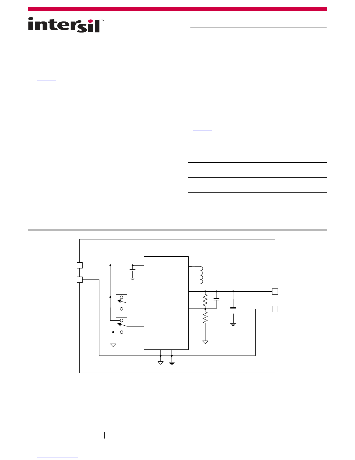
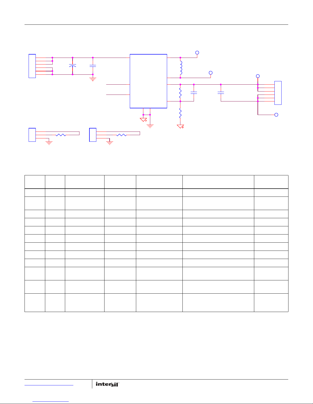
FIGURE 1. ISL9120IIA-EVZ BLOCK DIAGRAM
VOUT
VOUT
FB
VIN
VIN
BYP
ISL9120IIAZ
SGND
PGND
LX1
LX2
EN
GND
GND
ISL9120IIx-EVZ Evaluation Board User Guide
Description
The ISL9120 is a highly integrated buck-boost switching
regulator for systems using new battery chemistries. It uses
Intersil’s proprietary buck-boost algorithm to maintain voltage
regulation, while providing excellent efficiency and very low
output voltage ripple when the input voltage is close to the
output voltage. The ISL9120IIx-EVZ platforms allow quick
evaluation of the high performance features of the ISL9120
buck-boost regulator series.
Specifications
The boards are designed to operate under the following
conditions:
• Input voltage rating from 1.8V to 5.5V
• Resistor programmable output voltage on the ISL9120IIA-EVZ
• Fixed 3.3V output voltage on the ISL9120IIN-EVZ
• Up to 800mA output current (V
= 2.5V, V
IN
• Operating temperature range: -40°C to +85°C
OUT
= 3.3V)
Key Features
•Small, compact design
• Jumper selectable EN (enabled/disabled)
• Jumper selectable BYP (buck-boost/forced bypass)
• Connectors, test points and jumpers for easy probing
References
• ISL9120 Datasheet
Ordering Information
PART NUMBER DESCRIPTION
ISL9120IIN-EVZ Evaluation Board for ISL9120IINZ, fixed 3.3V
output
ISL9120IIA-EVZ Evaluation Board for ISL9120IIAZ, adjustable
output
May 28, 2015
UG023.1
1
CAUTION: These devices are sensitive to electrostatic discharge; follow proper IC Handling Procedures.
1-888-INTERSIL or 1-888-468-3774
Intersil (and design) is a trademark owned by Intersil Corporation or one of its subsidiaries.
All other trademarks mentioned are the property of their respective owners.
| Copyright Intersil Americas LLC 2015. All Rights Reserved
Page 2
User Guide 023
EN (2V/DIV)
V
OUT
(1V/DIV)
IL (500mA/DIV)
400µs/DIV
400µs/DIV
EN (2V/DIV)
V
OUT
(1V/DIV)
IL (500mA/DIV)
Functional Description
The ISL9120IIx-EVZ evaluation boards provide simple platforms
to demonstrate the feature of the ISL9120 buck-boost regulator.
The ISL9120IIN-EVZ is for the fixed 3.3V output IC ISL9120IINZ.
The ISL9120IIA-EVZ is for the adjustable output IC ISL9120IIAZ.
The evaluation boards have been functionally optimized for best
performance of the ISL9120 IC series. The input power and load
connections are provided through multipin connectors for high
current operations.
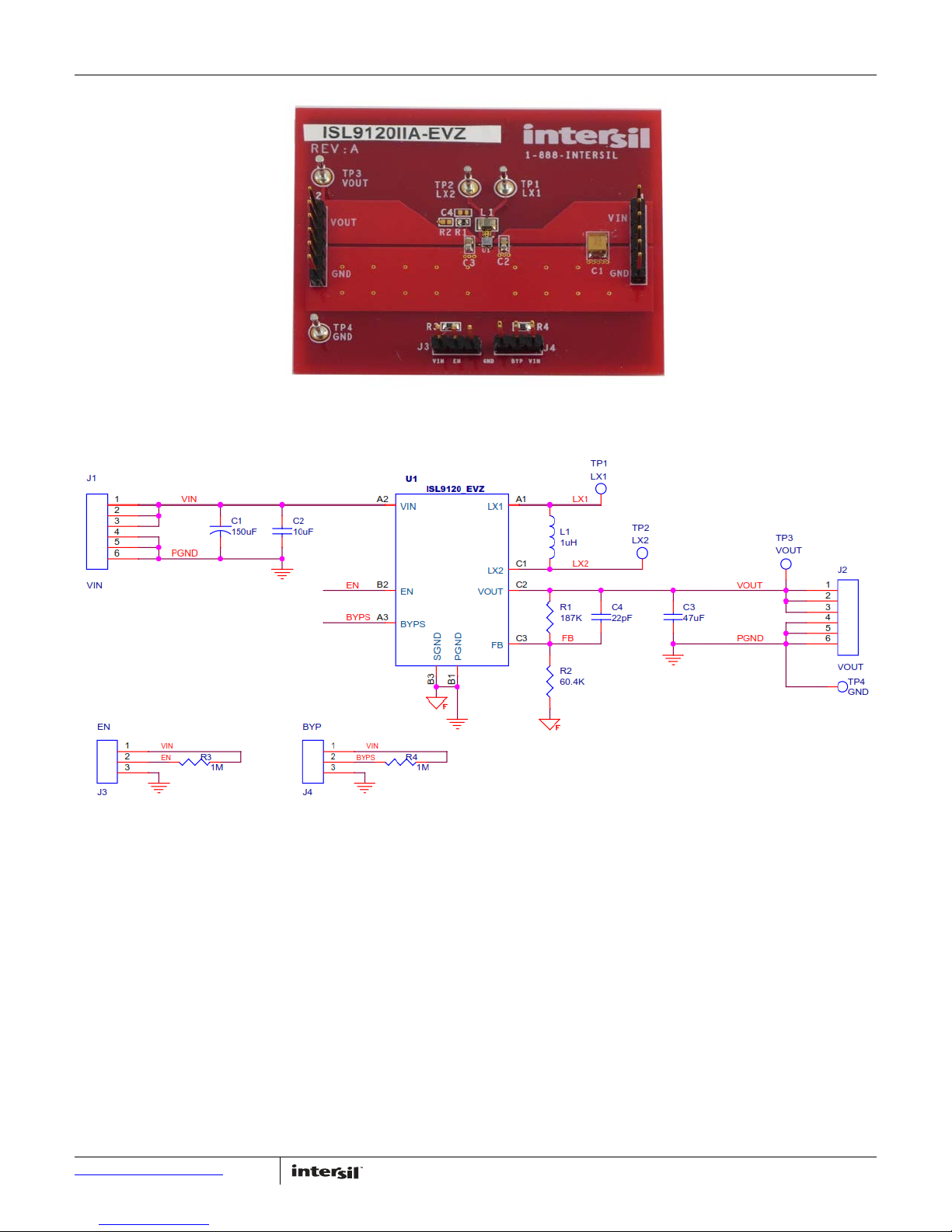
The ISL9120IIA-EVZ evaluation board schematic is shown in
Figure 5, on page 3
. The board’s enable function is controlled by
the on-board jumper header J3. Similarly, the forced bypass
function is controlled by the on-board jumper header J4. The
schematic for the ISL9120IIN-EVZ is shown in Figure 7
. The PCB
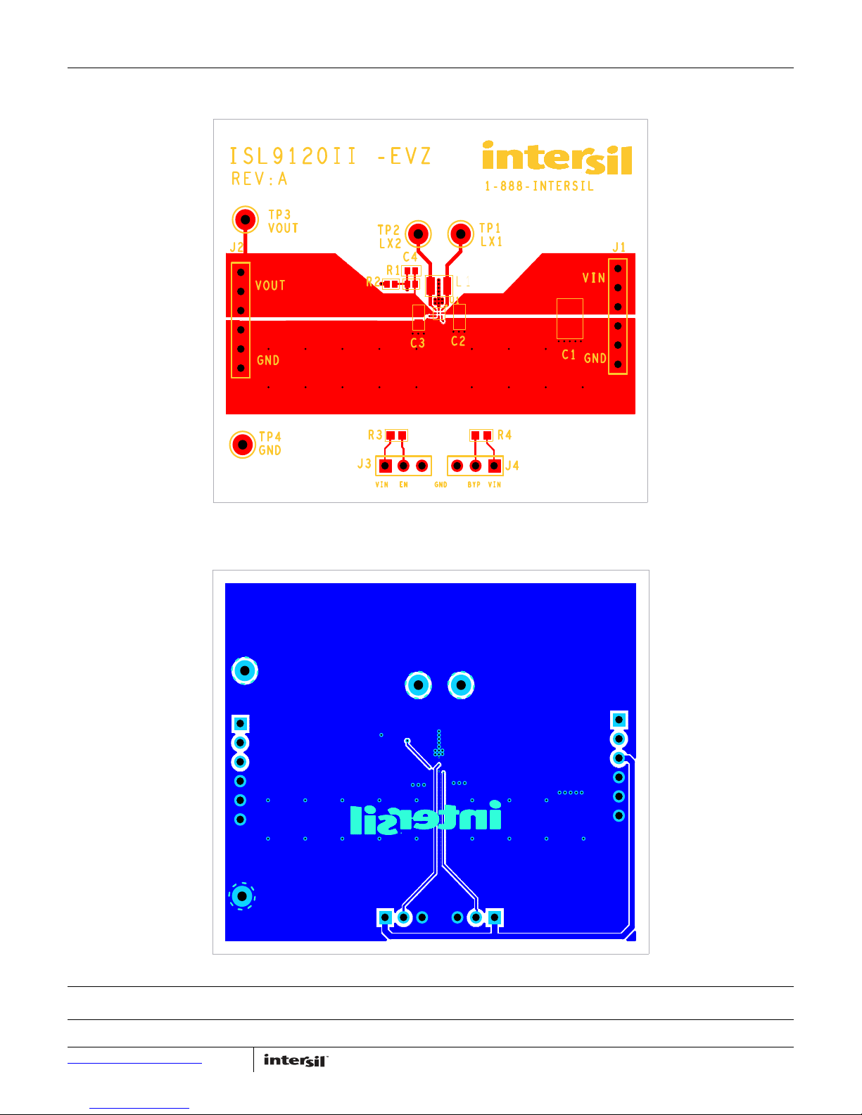
layout images for all layers are shown in Figures 8 and 9. The bill
of materials for the ISL9120IIA-EVZ are shown in Tab l e 2 on
page 4. The bill of materials for the ISL9120IIN-EVZ are shown in
Table 3 on pa ge 5 .
Operating Range
The VIN range of the boards is 1.8V to 5.5V. The V
ISL9120IIA-EVZ is 2V to 5V. The I
range of the boards is 0 to 1A.
OUT
The operating ambient temperature range is -40°C to +85°C.
range for the
OUT
TABLE 1. OUTPUT VOLTAGE PROGRAMMING For ISL9120IIA-EVZ
DESIRED OUTPUT VOLTAGE
(V)
2.0 124
2.5 88.7
3.0 68.1
3.3 60.4
3.4 57.6
4.0 46.4
4.5 40.2
5.0 35.7
RESISTOR VALUE
R
2
(k)
Quick Start Guide
For the ISL9120IIA-EVZ board, the default output voltage is set at
3.3V. Should other output voltages are desired, resistor R2 can
be changed to set to a desired voltage as shown in Table 1 (use a
resistor with 1% accuracy).
Refer to the following Quick Setup Guide to configure and power
up the board for proper operation
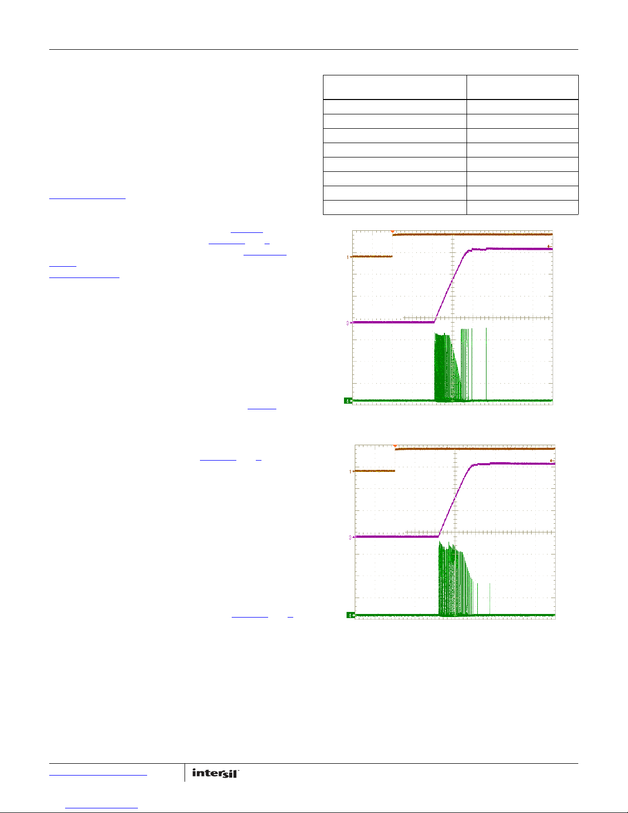
the expected waveforms are shown in Figures 2
Quick Setup Guide
1. Install jumper on J3, shorting EN to VIN.
2. Install jumper on J4, shorting BYP to GND.
3. Connect power supply to J1, with voltage setting between
1.8V and 5.5V.
4. Connect electronic load to J2.
5. Place scope probes on the V
points of interest.
6. Turn on the power supply.
7. Monitor the output voltage start-up sequence on the scope. The
waveforms will look similar to that shown in Figures 2 and 3.
8. Turn on the electronic load.
9. Measure the output voltage with the voltmeter. The voltage
should regulate within datasheet spec limits.
. During the power-on process,
and 3.
test point and other test
OUT
FIGURE 2.
FIGURE 3.
SOFT-START (V
SOFT-START (V
= 3V, V
IN
= 4V, V
IN
= 3.3V, NO LOAD)
OUT
= 3.3V, NO LOAD)
OUT
Recommended PCB Layout
Submit Document Feedback
2
Correct PCB layout is critical for proper operation of the ISL9120.
The input and output capacitors should be positioned as closely
to the IC as possible. The ground connections of the input and
output capacitors should be kept as short as possible and should
be on the component layer to avoid problems that are caused by
high switching currents flowing through PCB vias.
UG023.1
May 28, 2015
Page 3
User Guide 023
FIGURE 4. ISL9120IIA-EVZ EVALUATION BOARD
FIGURE 5. ISL9120IIA-EVZ EVALUATION BOARD SCHEMATIC
Submit Document Feedback
3
UG023.1
May 28, 2015
Page 4
User Guide 023
TABLE 2. ISL9120IIA-EVZ EVALUATION BOARD BILL OF MATERIALS
ITEM# QTY
1 1 U1 ISL9120IIAZ W3x3.9E; WLCSP Intersil ISL9120 Buck-boost Regulator
2 1 L1 1µH 0806 Power Inductor Toko DFE201610R
3 1 C1 150µF 1210 Capacitor, Tantalum ANY
4 1 C2 10µF/16V/X5R 0603 Capacitor, Generic ANY
5 1 C3 47µF/6.3V/X5R 0603 Capacitor, Generic ANY
6 1 C4 22pF 0402 Capacitor, Generic ANY
71 R1 187kΩ1% 0402 Resistor, Generic ANY
8 1 R2 60.4kΩ1% 0402 Resistor, Generic ANY
9 2 R3, R4 1MΩ5% 0603 Resistor, Generic ANY
10 2 J1, J2 HDR-6 HDR-6 Vert. Pin Header, 6-Pin, 0.1” Spacing,
11 2 J3, J4 HDR-3 HDR-3 Vert. Pin Header, 3-Pin, 0.1” Spacing,
12 4 TP1, TP2, TP3, TP4 Terminal Pin 0.052" hole Test Point, Terminal Pin Turret 0.082"
REFERENCE
DESIGNATOR PART TYPE FOOTPRINT DESCRIPTION MANUFACTURER
with Adjustable Output Voltage
series, 2.7A (typ), 80mΩ (typ)
Generic
Generic
[2110-2-00-80-00-00-07-0]
MANUFACTURING
INTERSIL
TOKO
ANY
ANY
MILL MAX
CORP.
Submit Document Feedback
4
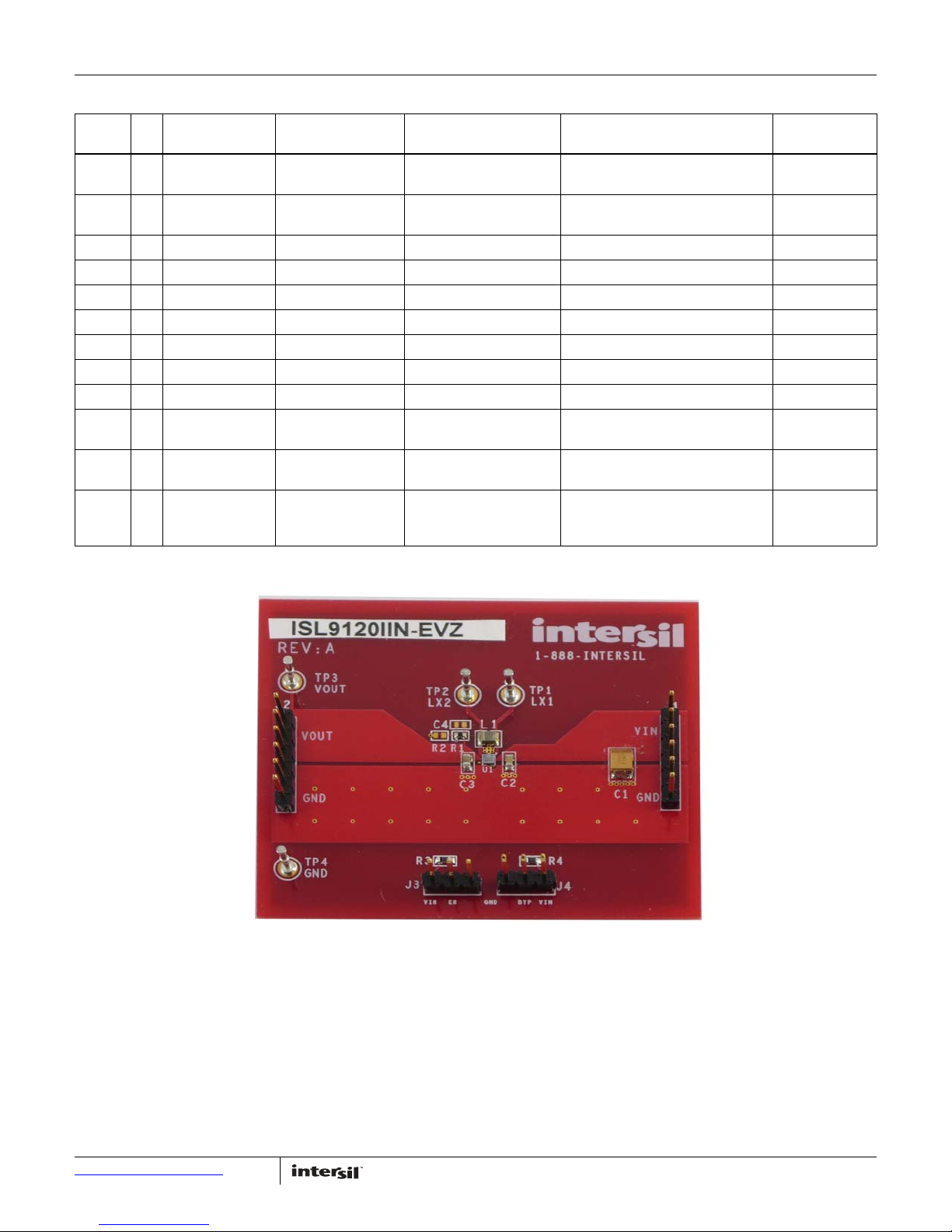
FIGURE 6. ISL9120IIN-EVZ EVALUATION BOARD
UG023.1
May 28, 2015
Page 5
User Guide 023
FB
VIN
PGND
EN
BYP
EN
VIN
BYP
VIN
VOUT
PGND
LX2
LX1
TP1
LX1
J3
EN
1
2
3
L1
1uH
J4
BYP
1
2
3
C1
150uF
J2
VOUT
1
2
3
4
5
6
R4
1M
TP4
GND
R3
1M
R2
DNP
R1
0
TP3
VOUT
C3
47uF
C2
10uF
U1
ISL9120_EVZ
LX1
A1
LX2
C1
VOUT
C2
FB
C3
VIN
A2
EN
B2
BYP
A3
SGNDB3PGND
B1
TP2
LX2
C4
DNP
J1
VIN
1
2
3
4
5
6
ISL9120IIN-EVZ Evaluation Board Schematic
FIGURE 7. ISL9120IIN-EVZ EVALUATION BOARD SCHEMATIC
TABLE 3. ISL9120IIN-EVZ EVALUATION BOARD BILL OF MATERIALS
REFERENCE
ITEM# QTY
DESIGNATOR PART TYPE FOOTPRINT DESCRIPTION MANUFACTURER
1 1 U1 ISL9120IINZ, W3x3.9E; WLCSP Intersil ISL9120 Buck-Boost Regulator INTERSIL
2 1 L1 1µH 0806 Power Inductor Toko DFE201610R
3 1 C1 150µF 1210 Capacitor, Tantalum ANY
4 1 C2 10µF/16V/X5R 0603 Capacitor, Generic ANY
5 1 C3 47µF/6.3.V/X5R 0603 Capacitor, Generic ANY
6 1 C4 DNP 0402 ANY
71 R1 0Ω 0402 Resistor, Generic ANY
8 1 R2 DNP 0402 ANY
9 2 R3, R4 1MΩ5% 0603 Resistor, Generic ANY
10 2 J1, J2 HDR-6 HDR-6 Vert. Pin Header, 6-Pin, 0.1” Spacing,
11 2 J3, J4 HDR-3 HDR-3 Vert. Pin Header, 3-Pin, 0.1” Spacing,
12 4 TP1, TP2, TP3, TP4 Terminal Pin 0.052" hole Test Point, Terminal Pin Turret 0.082"
5
Submit Document Feedback
series, 2.7A (typ), 80mΩ (typ)
TOKO
ANY
Generic
ANY
Generic
[2110-2-00-80-00-00-07-0]
MILL MAX
MANUFACTURING
CORP.
May 28, 2015
UG023.1
Page 6
PCB Layout
User Guide 023
FIGURE 8. TOP LAYER
Intersil Corporation reserves the right to make changes in circuit design, software and/or specifications at any time without notice. Accordingly, the reader is
cautioned to verify that the document is current before proceeding.
For information regarding Intersil Corporation and its products, see www.intersil.com
Submit Document Feedback
6
FIGURE 9. BOTTOM LAYER
UG023.1
May 28, 2015
 Loading...