®
www.BDTIC.com/Intersil
ISL90843
Quad Digital Controlled Potentiometers (XDCP™)
Data Sheet March 29, 2006
Low Noise, Low Power, I2C® Bus,
256 Taps
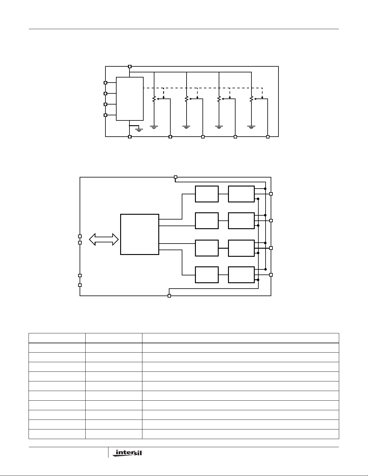
The ISL90843 integrates four digitally controlled
potentiometers (XDCP) on a monolithic CMOS integrated
circuit.
The digitally controlled potentiometers are implemented with
a combination of resistor elements and CMOS switches. The
position of the wipers are controlled by the user through the
2
I
C bus interface. Each potentiometer has an associated
Wiper Register (WR) that can be directly written to and read
by the user. The contents of the WR controls the position of
the wiper.
The DCPs can be used as a voltage divider in a wide variety
of applications including control, AC measurement, and
signal processing.
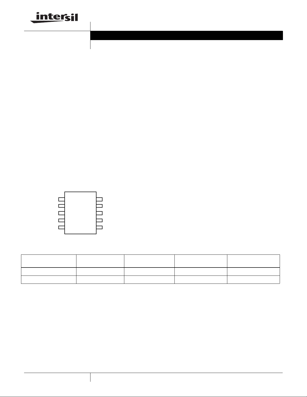
Pinout
ISL90843
(10 LD MSOP)
TOP VIEW
FN8095.2
Features
• Four potentiometers in one package
• 256 resistor taps–0.4% resolution
•I2C serial interface
- Two address pins allow up to four devices/bus
• Wiper resistance: 70Ω typical @ 3.3V
• Standby current <5µA max
• Power supply: 2.7V to 5.5V
•10kΩ or 50kΩ total resistance
• 10 Ld MSOP package
• Pb-free plus anneal product (RoHS compliant)
RW3
SCL
SDA
GND
RW2
1
2
3
4
5
RW0
10
V
9
CC
A1
8
A0
7
RW1
6
Ordering Information
PART NUMBER
(Note) PART MARKING
ISL90843WIU1027Z* DET 10 -40 to +85 10 Ld MSOP
ISL90843UIU1027Z* DES 50 -40 to +85 10 Ld MSOP
*Add "-TK" suffix for tape and reel.
NOTE: Intersil Pb-free plus anneal products employ special Pb-free material sets; molding compounds/die attach materials and 100% matte tin plate
termination finish, which are RoHS compliant and compatible with both SnPb and Pb-free soldering operations. Intersil Pb-free products are MSL
classified at Pb-free peak reflow temperatures that meet or exceed the Pb-free requirements of IPC/JEDEC J STD-020.
RESISTANCE OPTION
(kΩ)
TEMP RANGE
(°C)
PACKAGE
(Pb-Free)
1
CAUTION: These devices are sensitive to electrostatic discharge; follow proper IC Handling Procedures.
1-888-INTERSIL or 1-888-468-3774
XDCP is a trademark of Intersil Americas Inc. Copyright Intersil Americas Inc. 2005, 2006. All Rights Reserved
| Intersil (and design) is a registered trademark of Intersil Americas Inc.
All other trademarks mentioned are the property of their respective owners.

Functional Diagram
www.BDTIC.com/Intersil
ISL90843
V
CC
Block Diagram
SDA
SCL
SCL
SDA
A0
A1
2
C
I
INTERFACE
I2C
INTERFACE
GND R
POWER-UP,
INTERFACE,
CONTROL AND
STATUS LOGIC
R
H
R
L
W0
R
H
R
L
R
W1
V
CC
WR3
WR2
WR1
R
H
R
L
R
W2
DCP3
DCP2
DCP1
R
H
R
L
R
W3
R
W3
R
W2
R
W1
A1
A0
GND
WR0
Pin Descriptions
MSOP PIN SYMBOL DESCRIPTION
1 RW3 “Wiper” terminal of DCP3
2
2SCLI
3 SDA Serial data I/O for the I
4 GND Device ground pin
5 RW2 “Wiper” terminal of DCP2
6 RW1 “Wiper” terminal of DCP1
7 A0 Device address for the I
8 A1 Device address for the I
9V
CC
10 RW0 “Wiper” terminal of DCP0
C interface clock
Power supply pin
2
C interface
2
C interface
2
C interface
DCP0
R
W0
2
FN8095.2
March 29, 2006

ISL90843
www.BDTIC.com/Intersil
Absolute Maximum Ratings Recommended Operating Conditions
Storage Temperature . . . . . . . . . . . . . . . . . . . . . . . .-65°C to +150°C
Voltage at any Digital Interface Pin
with Respect to GND . . . . . . . . . . . . . . . . . . . . . -0.3V to V
. . . . . . . . . . . . . . . . . . . . . . . . . . . . . . . . . . . . . . . . -0.3V to +6V
V
CC
Voltage at any DCP Pin with
Respect to GND . . . . . . . . . . . . . . . . . . . . . . . . . . . . -0.3V to V
Lead Temperature (Soldering, 10s) . . . . . . . . . . . . . . . . . . . . . 300°C
I
(10s) . . . . . . . . . . . . . . . . . . . . . . . . . . . . . . . . . . . . . . . . . . ±6mA
W
CAUTION: Stresses above those listed in “Absolute Maximum Ratings” may cause permanent damage to the device. This is a stress only rating and operation of the
device at these or any other conditions above those indicated in the operational sections of this specification is not implied.
Analog Specifications Over recommended operating conditions unless otherwise stated.
SYMBOL PARAMETER TEST CONDITIONS MIN
R
TOTAL
R
W
C
W
VOLTAGE DIVIDER MODE (0V @ RLi; VCC @ RHi; measured at RWi, unloaded; i = 0, 1, 2, or 3)
(Note 6) Integral Non-Linearity -1 1 LSB
INL
(Note 5) Differential Non-Linearity Monotonic over all tap positions -0.5 0.5 LSB
DNL
ZSerror
(Note 3)
FSerror
(Note 4)
V
MATCH
(Note 7)
TC
(Note 8) Ratiometric Temperature Coefficient DCP register set to 80 hex ±4 ppm/°C
V
RH to RL Resistance W, U versions respectively 10, 50 kΩ
RH to RL Resistance Tolerance -20 +20 %
Wiper Resistance VCC = 3.3V @ 25°C 70 Ω
Potentiometer Capacitance (Note 15) 25 pF
Zero-Scale Error W option 0 1 7 LSB
Full-Scale Error W option -7 -1 0 LSB
DCP to DCP Matching Any two DCPs at same tap position, same
+0.3
CC
CC
U option 0 0.5 2
U option -2 -1 0
voltage at all RH terminals, and same voltage at
all RL terminals
Industrial . . . . . . . . . . . . . . . . . . . . . . . . . . . . . . . . . . -40°C to +85°C
V
. . . . . . . . . . . . . . . . . . . . . . . . . . . . . . . . . . . . . . . . 2.7V to 5.5V
CC
Power Rating of each DCP . . . . . . . . . . . . . . . . . . . . . . . . . . . .5mW
Wiper Current of each DCP . . . . . . . . . . . . . . . . . . . . . . . . . .±3.0mA
TYP
(NOTE 1) MAX UNITS
(Note 2)
(Note 2)
(Note 2)
(Note 2)
-2 2 LSB
(Note 2)
Operating Specifications Over the recommended operating conditions unless otherwise specified.
SYMBOL PARAMETER TEST CONDITIONS MIN
I
CC1
I
CC2
I
I
LkgDig
t
DCP
(Note 15)
Vpor Power-On Recall Voltage Minimum V
VCC Supply Current
(Volatile write/read)
VCC Supply Current
(Volatile write/read)
VCC current (standby) V
SB
Leakage Current, at Pins A0, A1,
SDA and SCL Pins
DCP Wiper Response Time SCL falling edge of last bit of DCP Data Byte to wiper
10k DCPs, f
Read and Write States)
50k DCPs, f
Read and Write States)
= +5.5V, 10k DCPs, I2C Interface in Standby State 2.8 mA
CC
= +5.5V, 50k DCPs, I2C Interface in Standby State 0.6 mA
V
CC
= +3.6V, 10k DCPs, I2C Interface in Standby State 1.9 mA
V
CC
= +3.6V, 50k DCPs, I2C Interface in Standby State 0.4 mA
V
CC
Voltage at pin from GND to V
change
= 400kHz; SDA = Open; (for I2C, Active,
SCL
= 400kHz; SDA = Open; (for I2C, Active,
SCL
CC
at which memory recall occurs 1.8 2.6 V
CC
3
TYP
(NOTE 1) MAX UNITS
3.8 mA
2.9 mA
-10 10 µA
1µs
FN8095.2
March 29, 2006
 Loading...