®
www.BDTIC.com/Intersil
Quad Digitally Controlled Potentiometers (XDCP™)
ISL90840
Data Sheet November 14, 2006
Low Noise, Low Power I2C® Bus, 256 Taps
The ISL90840 integrates four digitally controlled
potentiometers (XDCP) on a monolithic CMOS integrated
circuit.
The digitally controlled potentiometers are implemented with
a combination of resistor elements and CMOS switches. The
position of the wipers are controlled by the user through the
2
I
C bus interface. Each potentiometer has an associated
volatile Wiper Register (WR) that can be directly written to
and read by the user. The contents of the WR controls the
position of the wiper. When powered on the ISL90810’s
wiper will always commence at mid-scale (128 tap position).
The DCPs can be used as three-terminal potentiometers or
as two-terminal variable resistors in a wide variety of
applications including control, parameter adjustments, and
signal processing.
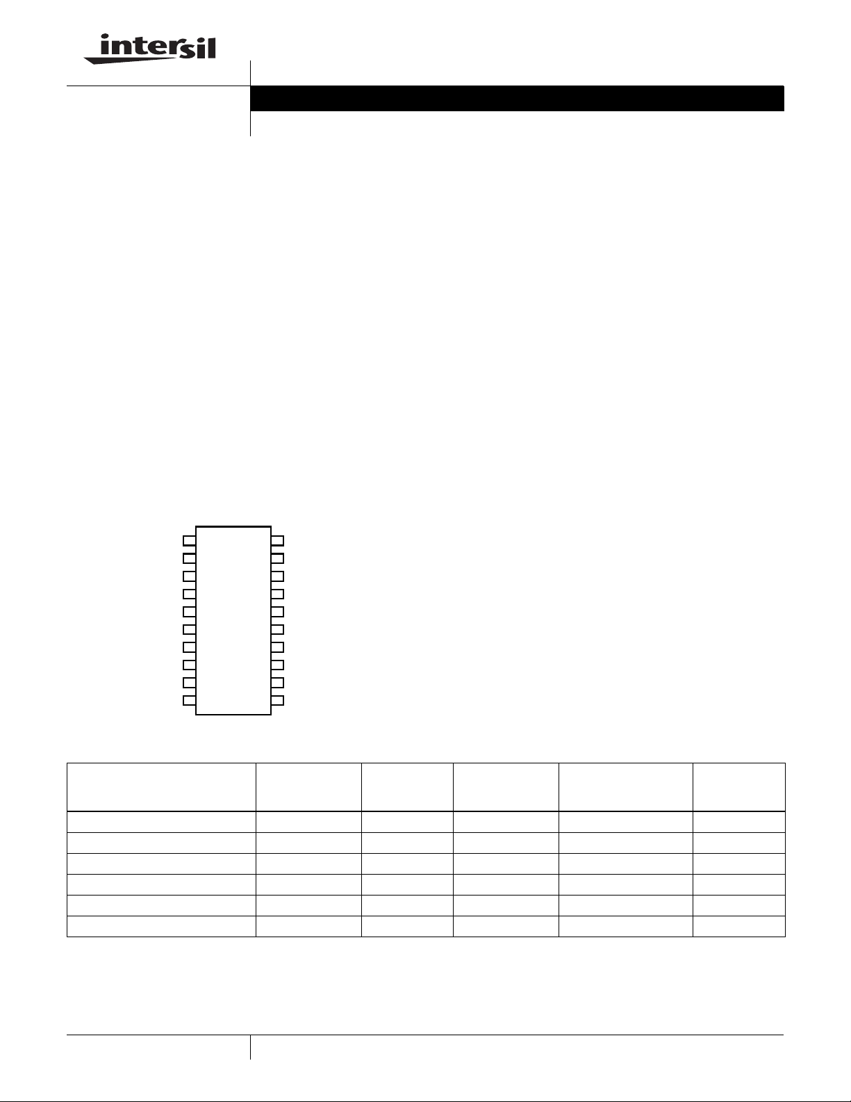
Pinout
ISL90840
(20 LD TSSOP)
TOP VIEW
FN8086.2
Features
• Four potentiometers in one package
• 256 resistor taps - 0.4% resolu ti o n
•I2C serial interface
- Three address pins, up to eight devices/bus
- Write/Read capability
• Power-on preset to mid-scale (128 tap position)
• Wiper resistance: 70Ω typical @ 3.3V
• Standby current <5µA max
• Power supply: 2.7V to 5.5V
•50kΩ, 10kΩ total resistance
• 20 Ld TSSOP package
• Pb-free plus anneal available (RoHS compliant)
RW0
RH3
RL3
RW3
A2
SCL
SDA
GND
RW2
RL2
RH2
1
2
3
4
5
6
7
8
9
10
20
RL0
19
RH0
18
D.N.C.
17
VCC
16
A1
15
A0
14
RH1
13
RL1
12
RW1
11
Ordering Information
RESIST-ANCE
OPTION
PART NUMBER PART MARKING
ISL90840UIV2027Z (Notes 1 and 2) ISL90840UI27Z 50k -40 to +85 20 Ld TSSOP (Pb-free) MDP0044
ISL90840UIV2027 ISL90840UI27 50k -40 to +85 20 Ld TSSOP MDP0044
ISL90840UAV2027Z (Notes 1 and 2) ISL90840UA27Z 50k -40 to +105 20 Ld TSSOP (Pb-free) MDP0044
ISL90840WIV2027Z (Notes 1 and 2) ISL90840WI27Z 10k -40 to +85 20 Ld TSSOP (Pb-free) MDP0044
ISL90840WIV2027 ISL90840WI27 10k -40 to +85 20 Ld TSSOP MDP0044
ISL90840WAV2027Z (Notes 1 and 2) ISL90840WA27Z 10k -40 to +105 20 Ld TSSOP (Pb-free) MDP0044
NOTES:
1. Intersil Pb-free plus anneal products employ special Pb-free material sets; molding compounds/die attach materials and 100% matte tin plate
termination finish, which are RoHS compliant and compatible with both SnPb and Pb-free soldering operations. Intersil Pb-free products are
MSL classified at Pb-free peak reflow temperatures that meet or exceed the Pb-free requirements of IPC/JEDEC J STD-020.
2. Add “T2” suffix for tape and reel.
(Ω)
TEMP
RANGE
(°C) PACKAGE PKG. DWG #
1
1-888-INTERSIL or 1-888-468-3774
CAUTION: These devices are sensitive to electrostatic discharge; follow proper IC Handling Procedures.
| Intersil (and design) and XDCP are registered trademarks of Intersil Americas Inc.
All other trademarks mentioned are the property of their respective owners.
Copyright Intersil Americas Inc. 2005-2006. All Rights Reserved

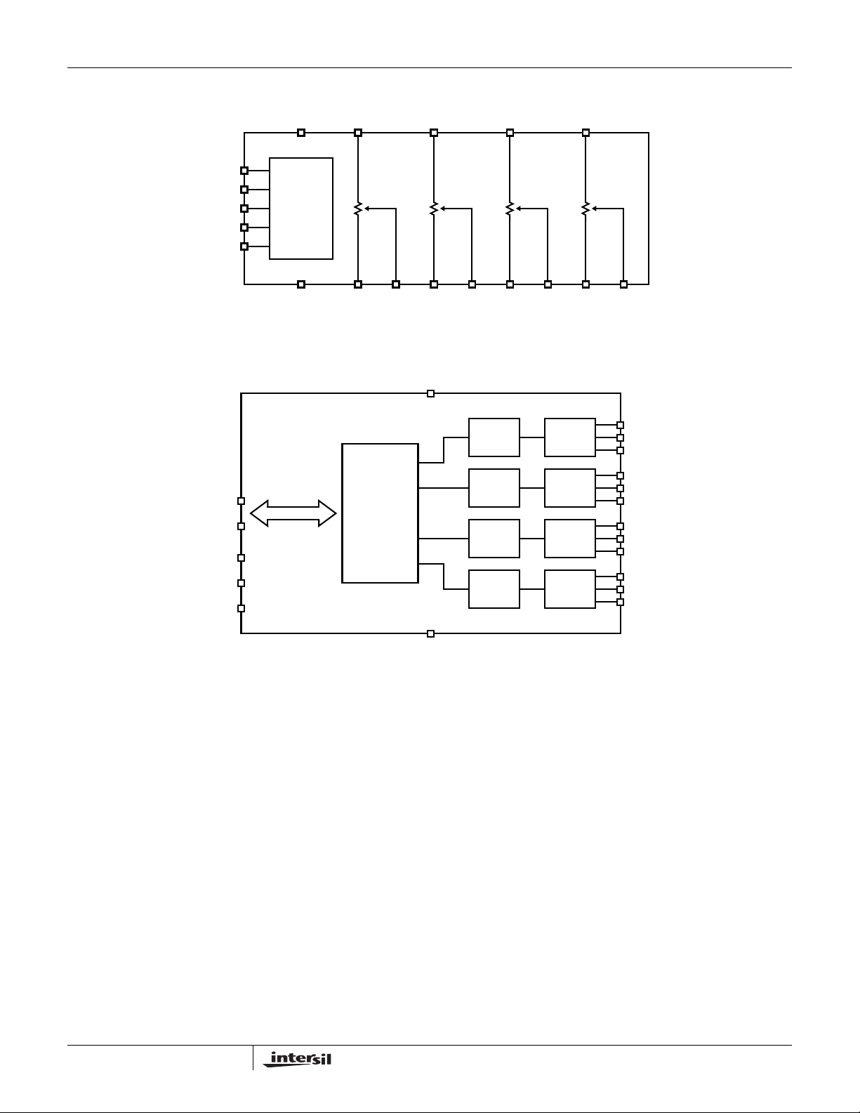
Functional Diagram
www.BDTIC.com/Intersil
ISL90840
Block Diagram
SCL
SDA
SDA
SCL
A2
A1
A0
A0
A1
A2
V
CC
I2C
INTERFACE
GND R
I2C INTERFACE
R
H0
R
L0
W0
POWER-UP,
INTERFACE,
CONTROL
AND STATUS
LOGIC
R
H1
R
L1
V
CC
R
H2
R
R
W1
L2
WR3
WR2
WR1
WR0
R
H3
R
R
W2
DCP3
DCP2
DCP1
DCP0
R
L3
W3
R
H3
R
W3
R
L3
R
H2
R
W2
R
L2
R
H1
R
W1
R
L1
R
H0
R
W0
R
L0
GND
2
FN8086.2
November 14, 2006

ISL90840
www.BDTIC.com/Intersil
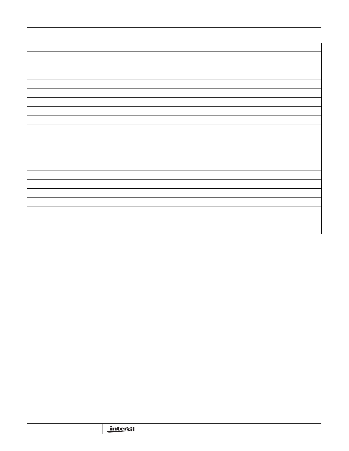
Pin Descriptions
TSSOP PIN SYMBOL DESCRIPTION
1 RH3 “High” terminal of DCP3
2 RL3 “Low” terminal of DCP3
3 RW3 “Wiper” terminal of DCP3
2
4 A2 Device address for the I
5SCLI
6 SDA Serial data I/O for the I
7 GND Device ground pin
8 RW2 “Wiper” terminal of DCP2
9 RL2 “Low” terminal of DCP2
10 RH2 “High” terminal of DCP2
11 RW1 “Wiper” terminal of DCP1
12 RL1 “Low” terminal of DCP1
13 RH1 “High” terminal of DCP1
14 A0 Device address for the I
15 A1 Device address for the I
16 VCC Power supply pin
17 D.N.C. Do not connect
18 RH0 “High” terminal of DCP0
19 RL0 “Low” terminal of DCP0
20 RW0 “Wiper” terminal of DCP0
2
C interface clock
C interface
2
C interface
2
C interface
2
C interface
3
FN8086.2
November 14, 2006

ISL90840
www.BDTIC.com/Intersil
Absolute Maximum Ratings Thermal Information
Storage Temperature. . . . . . . . . . . . . . . . . . . . . . . .-65°C to +150°C
Voltage at Any Digital Interface Pin
With Respect to V
. . . . . . . . . . . . . . . . . . . . . . . . . . . . . . . . . . . . . . . .-0.3V to +6V
V
CC
Voltage at Any DCP Pin
With Respect to V
Lead Temperature (Soldering, 10s) . . . . . . . . . . . . . . . . . . . .+300°C
I
(10s) . . . . . . . . . . . . . . . . . . . . . . . . . . . . . . . . . . . . . . . . . . ±6mA
W
Latchup . . . . . . . . . . . . . . . . . . . . . . . . . Class II, Level A @ +105°C
ESD
HBM . . . . . . . . . . . . . . . . . . . . . . . . . . . . . . . . . . . . . . . . . . . 2.5kV
CAUTION: Stresses above those listed in “Absolute Maximum Ratings” may cause permanent damage to the device. This is a stress only rating and operation of the
device at these or any other conditions above those indicated in the operational sections of this specification is not implied.
NOTES:
3. θ
is measured with the component mounted on a high effective thermal conductivity test board in free air. See Tech Brief TB379 for details.
JA
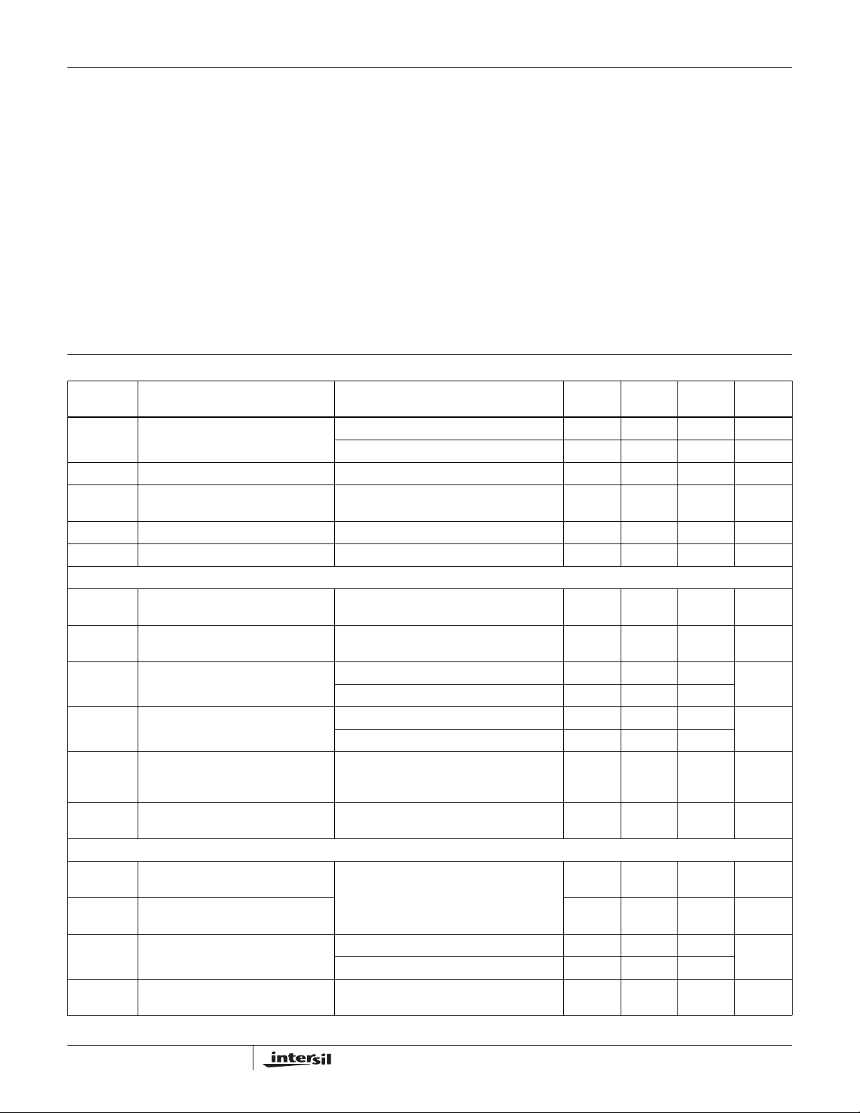
Analog Specifications Over recommended operating conditions unless otherwise stated.
SYMBOL PARAMETER TEST CONDITIONS MIN
R
TOTAL
R
W
C
H/CL/CW
I
LkgDCP
VOLTAGE DIVIDER MODE (0V @ R
INL
(Note 9)
DNL
(Note 8)
ZSerror
(Note 6)
FSerror
(Note 7)
MATCH
TC
V
RINL
RDNL
Roffset
MATCH
V
(Note 10)
(Note 11)
RESISTOR MODE (Measurements between R
(Note 15)
(Note 14)
(Note 13)
R
(Note 16)
. . . . . . . . . . . . . . . . . . . .-0.3V to VCC+0.3V
SS
. . . . . . . . . . . . . . . . . . . . . . . . -0.3V to V
SS
RH to RL resistance W option 10 kΩ
U option 50 kΩ
to RL resistance tolerance -20 +20 %
R
H
Wiper resistance VCC = 3.3V @ +25°C,
wiper current = V
Potentiometer capacitance (Note 18) 10/10/25 pF
Leakage on DCP pins (Note 18) Voltage at pin from GND to V
i; VCC @ RHi; measured at RWi, unloaded; i = 0, 1, 2, or 3)
L
Integral non-linearity -1 1 LSB
Differential non-linearity Monotonic over all tap positions -0.5 0.5 LSB
Zero-scale error W option 0 1 7 LSB
U option 0 0.5 2
Full-scale error W option -7 -1 0 LSB
U option -2 -1 0
DCP to DCP matching Any two DCPs at same tap position, same
voltage at all RH terminals, and same voltage
at all R
Ratiometric temperature coefficient DCP register set to 80 hex ±4 ppm/°C
i and RLi with RHi not connected, or between RWi and RHi with RLi not connected. i = 0, 1, 2 or 3)
W
Integral non-linearity DCP register set between 20 hex and FF
hex; monotonic over all tap positions
Differential non-linearity -0.5 0.5 MI
Offset W option 0 1 7 MI
U option 0 0.5 2
DCP to DCP matching Any two DCPs at the same tap position with
the same terminal voltages
CC
terminals
L
Thermal Resistance (Typical, Note 3)
20 Ld TSSOP Package . . . . . . . . . . . . . . . . . . . . . . 90
Maximum Junction Temperature (Plastic Package). . . . . . . .+150°C
Recommended Operating Conditions
Industrial . . . . . . . . . . . . . . . . . . . . . . . . . . . . . . . . . .-40°C to +85°C
Automotive. . . . . . . . . . . . . . . . . . . . . . . . . . . . . . . .-40°C to +105°C
. . . . . . . . . . . . . . . . . . . . . . . . . . . . . . . . . . . . . . . . 2.7V to 5.5V
V
CC
Power Rating. . . . . . . . . . . . . . . . . . . . . . . . . . . . . . . . . . . . . . .5mW
Wiper Current . . . . . . . . . . . . . . . . . . . . . . . . . . . . . . . . . . . .±3.0mA
TYP
(NOTE 4) MAX UNIT
70 200 Ω
CC/RTOTAL
CC
-2 2 LSB
-1 1 MI
-2 2 MI
0.1 1 µA
θ
JA
(Note 5)
(Note 5)
(Note 5)
(Note 5)
(Note 5)
(Note 12)
(Note 12)
(Note 12)
(Note 12)
(°C/W)
4
FN8086.2
November 14, 2006
 Loading...