®
www.BDTIC.com/Intersil
ISL90727, ISL90728
Single Volatile 128-Tap XDCP
Data Sheet August 2, 2006
Digitally Controlled Potentiometer
(XDCP™)
The Intersil ISL90727 and ISL90728 are digitally controlled
potentiometers (XDCP). Each device consists of a resistor
array, wiper switches, and a control section. The wiper
position is controlled by an I
2
C interface.
The potentiometer is implemented by a resistor array
composed of 127 resistive elements and a wiper switching
network. Between each element and at either end are tap
points accessible to the wiper terminal. The position of the
wiper element is controlled by the SDA and SCL inputs.
The device can be used in a wide variety of applications
including:
• Mechanical potentiometer replacement
• Transducer adjustment of pressure, temperature, position,
chemical, and optical sensors
• RF amplifier biasing
• LCD brightness and contrast adjustment
• Gain control and offset adjustment
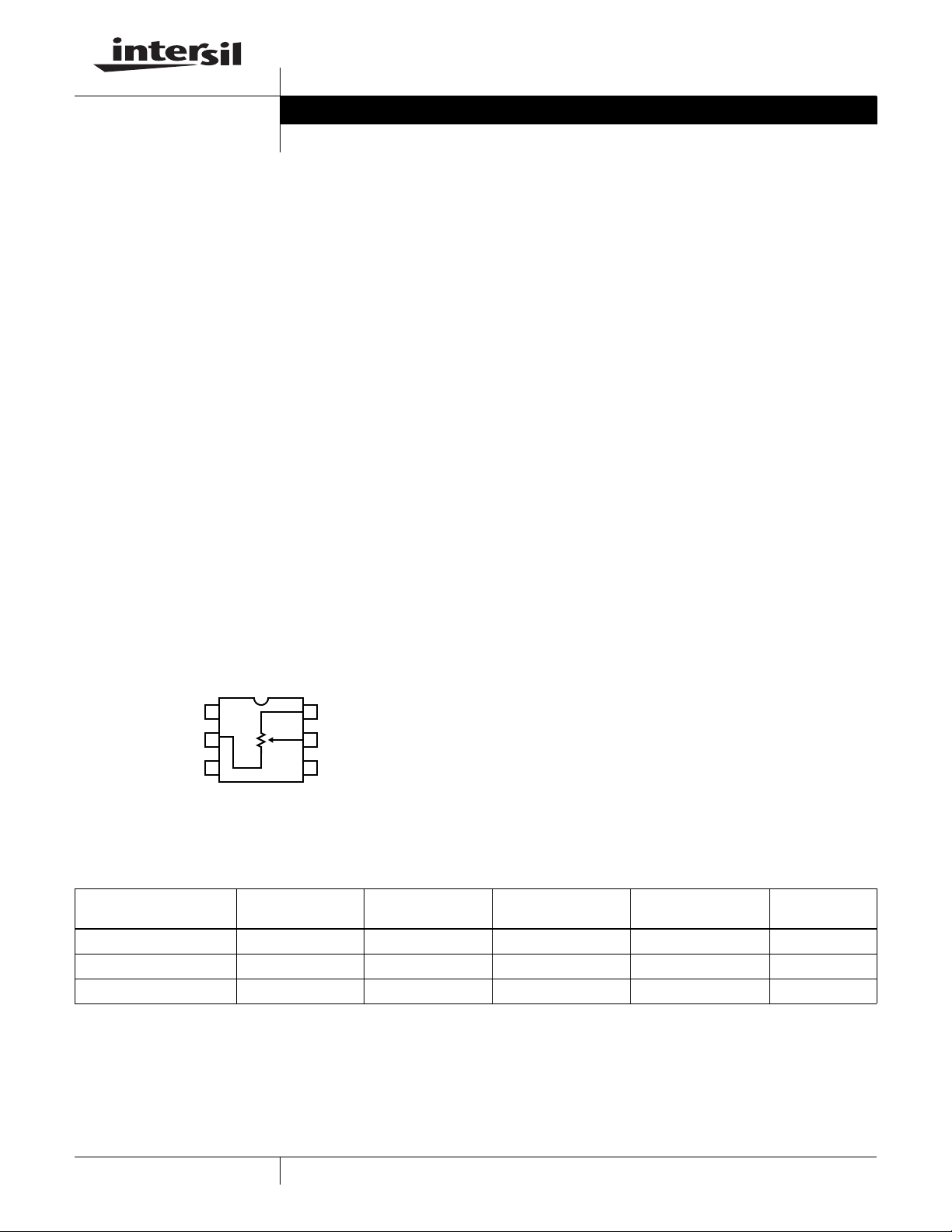
Pinout
ISL90727, ISL90728
(6 LD SC-70)
TOP VIEW
FN8247.4
Features
• Volatile Solid-State Potentiometer
2
•I
C Serial Bus Interface
• DCP Terminal Voltage, 2.7V to 5.5V
•Low Tempco
- Rheostat - 45 ppm/
- Divider - 15 ppm/°C typical
• 128 Wiper Tap Poin ts
- Wiper resistance 70Ω typ at V
• Low Power CMOS
- Active current, 200µA max
- Standby current, 500nA max
• Available R
TOTAL
• Power on Preset to Midscale
• Direct Replacement for AD5247
• Packaging
- 6 Ld SC-70
• Pb-Free Plus Anneal Available (RoHS Compliant)
°C typical
= 3.3V
CC
Values = 50kΩ, 10kΩ
VDD
GND
SCL
1
2
3
6
RH
5
RW
SDA
4
Ordering Information
PART NUMBER
(See Notes 1, 2) PART MARKING R
ISL90727WIE627Z-TK ANH 10 -40 to +85 6 Ld SC-70 P6.049
ISL90727UIE627Z-TK ANI 50 -40 to +85 6 Ld SC-70 P6.049
ISL90728WIE627Z-TK CCF 10 -40 to +85 6 Ld SC-70 P6.049
NOTES:
1. Intersil Pb-free plus anneal products employ special Pb-free material sets; molding compounds/die attach materials and 100% matte tin plate
termination finish, which are RoHS compliant and compatible with both SnPb and Pb-free soldering operations. Intersil Pb-free products are
MSL classified at Pb-free peak reflow temperatures that meet or exceed the Pb-free requirements of IPC/JEDEC J STD-020
2. ISL90727 has an I
2
C address 5Ch and ISL90728 has an I2C address 7Ch
TOTAL
(kΩ)
TEMP RANGE
(°C)
PACKAGE
(Pb-Free) PKG. DWG. #
1
CAUTION: These devices are sensitive to electrostatic discharge; follow proper IC Handling Procedures.
1-888-INTERSIL or 1-888-468-3774
XDCP is a trademark of Intersil Americas Inc. Copyright Intersil Americas Inc. 2005-2006. All Rights Reserved
| Intersil (and design) is a registered trademark of Intersil Americas Inc.
All other trademarks mentioned are the property of their respective owners.

ISL90727, ISL90728
www.BDTIC.com/Intersil
Pin Descriptions
PIN NUMBER SYMBOL DESCRIPTION
1 VDD Supply Voltage
2 GND Ground
3 SCL Open drain Serial Clock input
4 SDA Open drain Serial Data I/O
5 RW Potentiometer Wiper Terminal
6 RH Potentiometer High Terminal
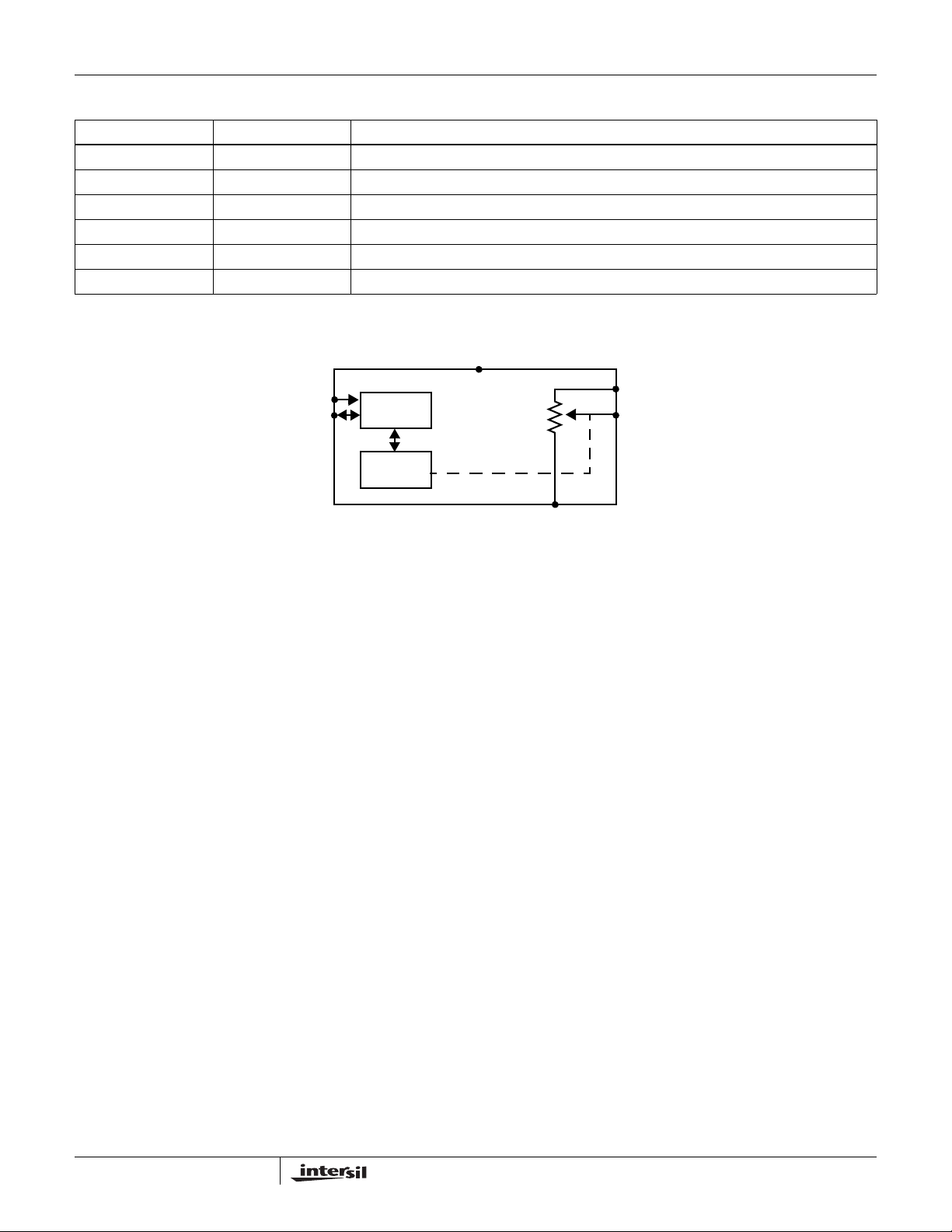
Block Diagram
VDD
SCL
SDA
I2C
INTERFACE
WIPER
REGISTER
RH
RW
RL
GND
2
FN8247.4
August 2, 2006

ISL90727, ISL90728
www.BDTIC.com/Intersil
Absolute Maximum Ratings Recommended Operating Conditions
Storage Temperature. . . . . . . . . . . . . . . . . . . . . . . .-65°C to +150°C
Voltage at any Digital Interface Pin
with Respect to V
. . . . . . . . . . . . . . . . . . . . . . . . . . . . . . . . . . . . . . . .-0.3V to +7V
V
CC
Voltage at any DCP Pin with
Respect to V
. . . . . . . . . . . . . . . . . . . . . . -0.3V to VCC+0.3
SS
. . . . . . . . . . . . . . . . . . . . . . . . . . . . -0.3V to V
SS
CC
Lead Temperature (soldering, 10s) . . . . . . . . . . . . . . . . . . . . .300°C
I
(10s) . . . . . . . . . . . . . . . . . . . . . . . . . . . . . . . . . . . . . . . . . . ±6mA
W
Latchup . . . . . . . . . . . . . . . . . . . . . . . . . . . Class II, Level B at 85°C
ESD . . . . . . . . . . . . . . . . . . . . . . . . . . . . . >2kV Human Body Model
CAUTION: Stresses above those listed in “Absolute Maximum Ratings” may cause permanent damage to the device. This is a stress only rating and operation of the
device at these or any other conditions above those indicated in the operational sections of this specification is not implied .
Analog Specifications Over recommended operating conditions unless otherwise stated.
SYMBOL PARAMETER TEST CONDITIONS MIN
R
TOTAL
RH to RL Resistance W option 10 kΩ
U option 50 kΩ
to RL Resistance Tolerance -20 +20 %
R
H
R
W
C
H/CL/CW
I
LkgDCP
Wiper Resistance VCC = 3.3V @ 25°C 85 200 Ω
Potentiometer Capacitance 10/10/
Leakage on DCP Pins
Voltage at pin from GND to V
VOLTAGE DIVIDER MODE
INL Integral Non-linearity -1 ±0.2 1 LSB
DNL Differential Non-linearity Monotonic over all tap positions W option -1 ±0.1 1 LSB
ZSerror
(Note 5)
FSerror
(Note 6)
(Note 12) Ratiometric Temperature Coefficient DCP Register set to 80 hex ±15 ppm/°C
TC
V
Zero-scale Error W option 0 1 3 LSB
U option 0 0.5 1
Full-scale Error W option -3 -1 0 LSB
U option -1 -0.5 0
RESISTOR MODE
RINL
(Note 10)
RDNL
(Note 9)
Integral Non-linearity DCP register set between 20 hex and FF hex.
Monotonic over all tap positions
Differential Non-linearity DCP register set between 20 hex
and FF hex. Monotonic over all tap
positions
Roffset
Offset W option 0 1 3 MI
(Note 8)
U option 0 0.5 1 MI
TC
Resistance Temperature Coefficient DCP register set between 20 hex and FF hex ±45 ppm/°C
R
(Notes 11, 12)
Industrial . . . . . . . . . . . . . . . . . . . . . . . . . . . . . . . . . .-40°C to +85°C
. . . . . . . . . . . . . . . . . . . . . . . . . . . . . . . . . . . . . . . . 2.7V to 5.5V
V
CC
Power Rating of Each DCP . . . . . . . . . . . . . . . . . . . . . . . . . . . .5mW
TYP
(Note 3) MAX UNIT
pF
25
CC
0.1 µA
(Note 4)
(Note 4)
U option -1 ±0.1 1 LSB
(Note 4)
(Note 4)
(Note 4)
-2 ±0.25 2 MI
(Note 7)
W option -1 ±0.1 1 MI
(Note 7)
U option -1 ±0.1 1 MI
(Note 7)
(Note 7)
(Note 7)
3
FN8247.4
August 2, 2006
 Loading...