®
www.BDTIC.com/Intersil
ISL90461
Digitally Controlled Potentiometer (XDCP™)
Data Sheet October 14, 2005
Single Volatile 32-Tap XDCP
The Intersil ISL90461 is a digitally controlled potentiometer
(XDCP). Configured as a variable resistor, the device
consists of a resistor array, wiper switches, a control section,
and volatile memory. The wiper position is controlled by a 2pin Up /Down interface.
The potentiometer is implemented by a resistor array
composed of 31 resistive elements and a wiper switching
network. Between each element and at either end are tap
points accessible to the wiper terminal. The position of the
wiper element is controlled by the CS
The device can be used in a wide variety of applications
including:
• LCD contrast control
• Parameter and bias adjustments
• Industrial and Automotive Control
• Transducer adjustment of pressure, temperature, position,
chemical, and optical sensors
• Laser Diode driver biasing
• Gain control and offset adjustment
and U/D inputs.
FN8229.3
Features
• Volatile solid-state potentiometer
• 2-pin UP/DN interface
• DCP terminal voltage, 2.7V to 5.5V
• Tempco 35 ppm/
°C typical
• 32 wiper tap points
• Low power CMOS
- Active current, 25µA max.
- Supply current 0.3µA
• Available R
• Temperature Range
values = 10kΩ, 50kΩ, 100kΩ
TOTAL
-40°C to +85°C
• Packages
- 6 Ld SC-70, SOT-23
• Pb-Free Plus Anneal Available (RoHS Compliant)
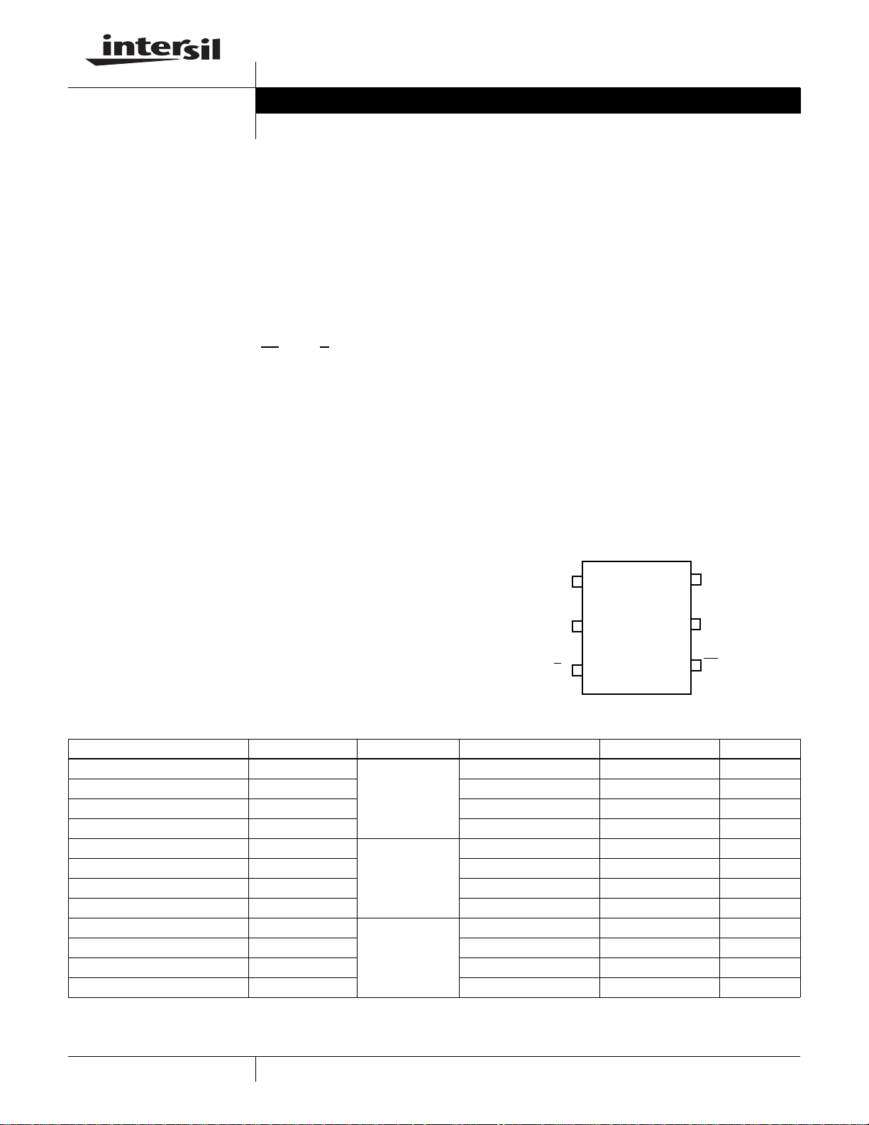
Pinout
ISL90461
(SOT-23, SC-70)
TOP VIEW
VDD
RH
GND
U/D
RL
CS
Ordering Information
PAR T N UM BE R PAR T M AR KI NG R
ISL90461WIE627-TK AJP 10 -40 to +85 6 Ld SC-70 P6.049
ISL90461WIE627Z-TK (See Note) DEE -40 to +85 6 Ld SC-70 (Pb-free) P6.049
ISL90461WIH627-TK AJY -40 to +85 6 Ld SOT-23 P6.064
ISL90461WIH627Z-TK (See Note) DEF -40 to +85 6 Ld SOT-23 (Pb-free) P6.064
ISL90461UIE627-TK AJR 50 -40 to +85 6 Ld SC-70 P6.049
ISL90461UIE627Z-TK (See Note) DEC -40 to +85 6 Ld SC-70 (Pb-free) P6.049
ISL90461UIH627-TK AKA -40 to +85 6 Ld SOT-23 P6.064
ISL90461UIH627Z-TK (See Note) DED -40 to +85 6 Ld SOT-23 (Pb-free) P6.064
ISL90461TIE627-TK AJQ 100 -40 to +85 6 Ld SC-70 P6.049
ISL90461TIE627Z-TK (See Note) DEA -40 to +85 6 Ld SC-70 (Pb-free) P6.049
ISL90461TIH627-TK AJZ -40 to +85 6 Ld SOT-23 P6.064
ISL90461TIH627Z-TK (See Note) DEB -40 to +85 6 Ld SOT-23 (Pb-free) P6.064
NOTE: Intersil Pb-free plus anneal products employ special Pb-free material sets; molding compounds/die attach materials and 100% matte tin plate termination finish, which are
RoHS compliant and compatible with both SnPb and Pb-free soldering operations. Intersil Pb-free products are MSL classified at Pb-free peak reflow temperatures that meet or exceed
the Pb-free requirements of IPC/JEDEC J STD-020
(K) TEMP RANGE (°C) PACKAGE PKG. DWG. #
TOTAL
1
CAUTION: These devices are sensitive to electrostatic discharge; follow proper IC Handling Procedures.
1-888-INTERSIL or 1-888-468-3774
XDCP is a trademark of Intersil Americas Inc. Copyright Intersil Americas Inc. 2005. All Rights Reserved
| Intersil (and design) is a registered trademark of Intersil Americas Inc.
All other trademarks mentioned are the property of their respective owners.

ISL90461
www.BDTIC.com/Intersil
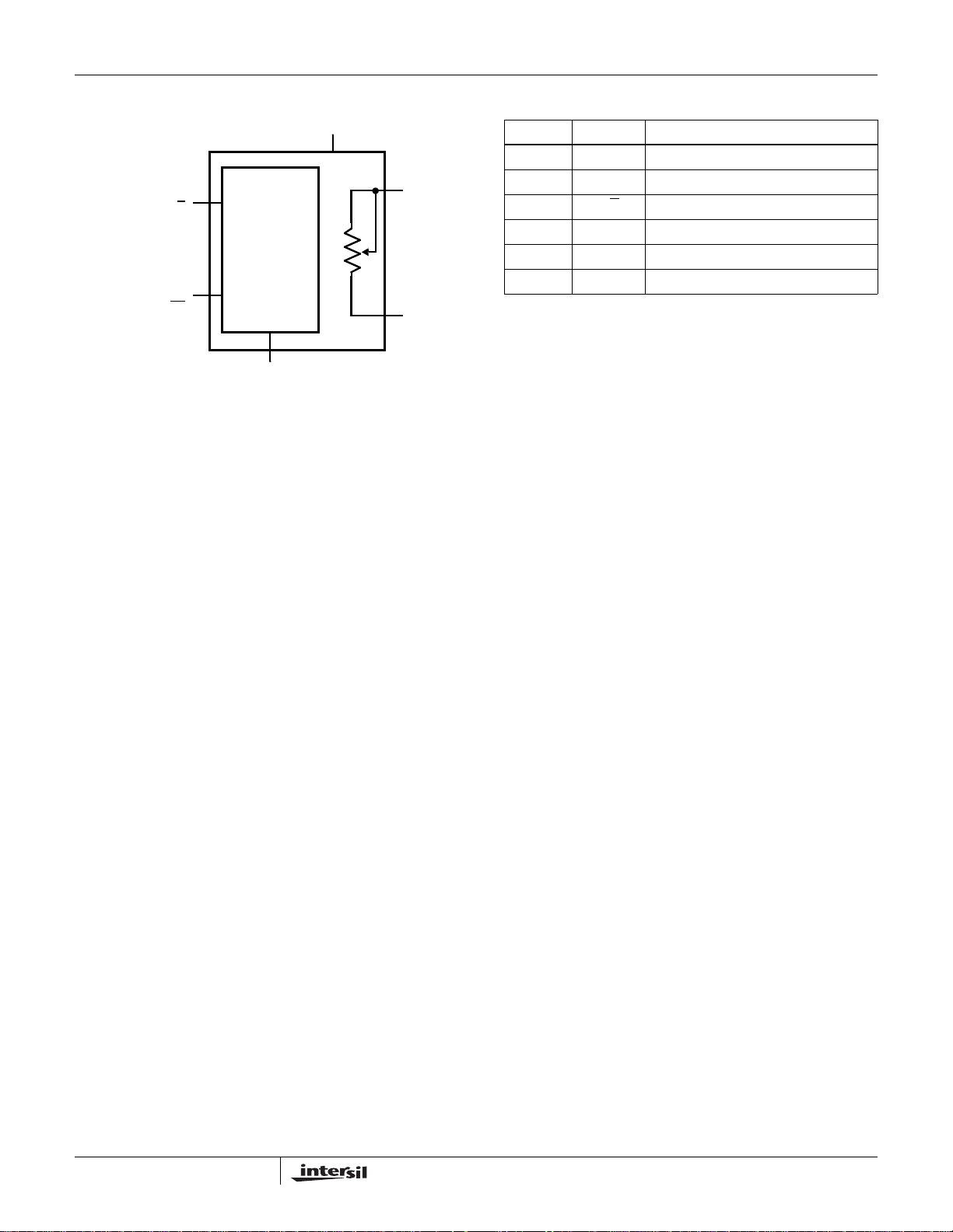
Block Diagram
UP/DOWN
(U/D
)
DEVICE SELECT
)
(CS
CONTROL
AND
MEMORY
GND (GROUND)
GENERAL
VCC
RH
RL
Pin Descriptions
6-PIN SYMBOL DESCRIPTION
1 VDD Supply voltage
2 GND Ground
3U/D
4 CS Chip select
5 RL Low terminal
6 RH High terminal/ Wiper terminal
Up - Down
2
FN8229.3
October 14, 2005

ISL90461
www.BDTIC.com/Intersil
Absolute Maximum Ratings Recommended Operating Conditions
Storage temperature . . . . . . . . . . . . . . . . . . . . . . . .-65°C to +150°C
Voltage on CS
, U/D and VCC
with respect to GND . . . . . . . . . . . . . . . . . . . . . . . . . . . -1V to +7V
Lead temperature (soldering 10s) . . . . . . . . . . . . . . . . . . . . . .300°C
(10s) . . . . . . . . . . . . . . . . . . . . . . . . . . . . . . . . . . . . . . . . . . ±6mA
I
W
Power rating. . . . . . . . . . . . . . . . . . . . . . . . . . . . . . . . . . . . . . . .1mW
CAUTION: Stresses above those listed in “Absolute Maximum Ratings” may cause permanent damage to the device. This is a stress only rating and operation of the
device at these or any other conditions above those indicated in the operational sections of this specification is not implied.
Potentiometer Specifications Over recommended operating conditions unless otherwise stated.
SYMBOL PARAMETER TEST CONDITIONS/NOTES MIN
R
TOT
V
R
R
W
I
W
CH/CL/C
NOTES:
1. Absolute linearity is utilized to determine actual wiper voltage versus expected voltage = (R
n = 1 .. 29 only
2. Relative linearity is a measure of the error in step size between taps = R
3. 1 Ml = Minimum Increment = R
4. Typical values are for T
End to end resistance W version 8 10 12 kΩ
U version 405060kΩ
T version 80 100 120 kΩ
RH, RL terminal voltages 0 V
Noise Ref: 1kHz -120 dBV
Wiper Resistance 600 Ω
Wiper Current 0.6 mA
Resolution 132Taps
Absolute linearity (Note 1) R
Relative linearity (Note 2) R
temperature coefficient ±35 ppm/°C
R
TOTAL
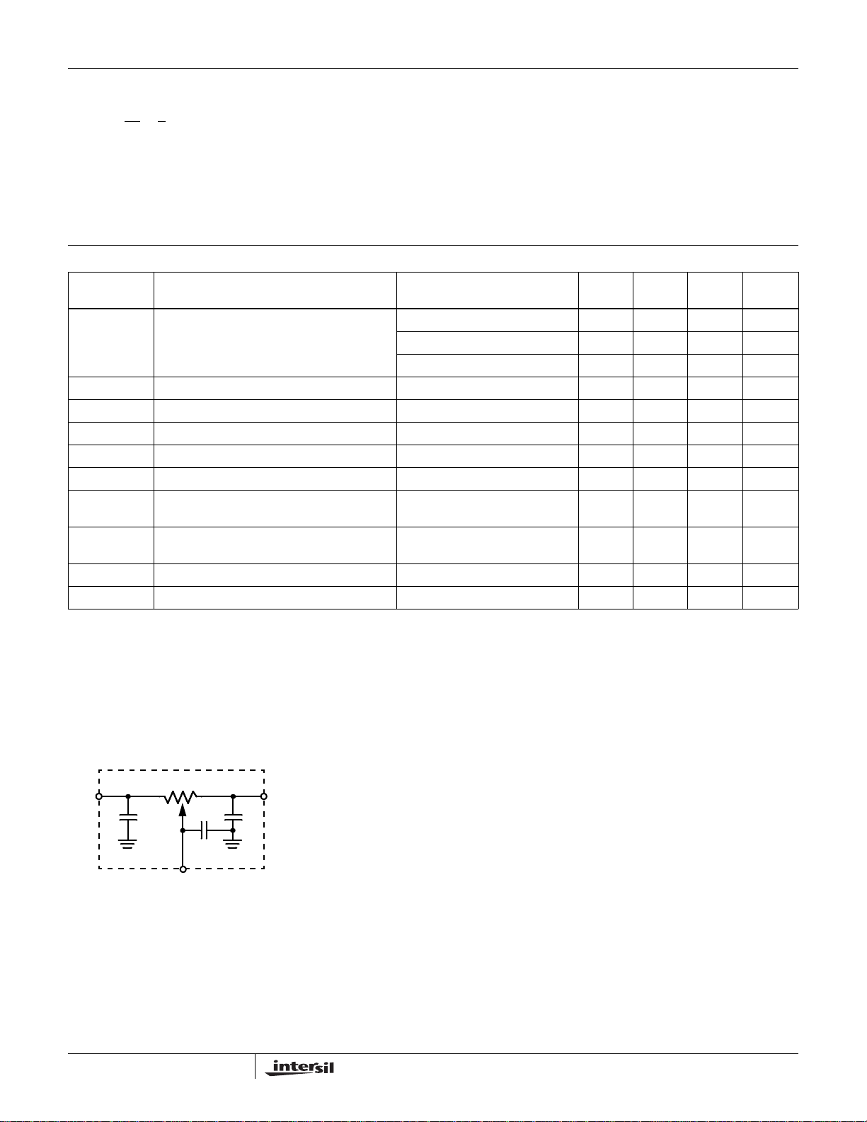
Potentiometer capacitances See equivalent circuit 10/10/25 pF
W
/31.
TOT
= 25°C and nominal supply voltage.
A
H(n)(actual)-RH(n)(expected)
H(n+1)
Temperature Range (Industrial) . . . . . . . . . . . . . . . . .-40°C to +85°C
Supply Voltage (V
) . . . . . . . . . . . . . . . . . . . . . . . . . . 2.7V to 5.5V
CC
TYP
(Note 4) MAX UNIT
CC
±1 MI
(Note 3)
-[R
H
]±0.5MI
H(n)+MI
(n+1)
(actual) - R
(n)
H
-[R
+ Ml] = ±0.5 Ml, n = 1 .. 29 only.
(n)
H
(expected)) = ±1 Ml Maximum.
(n)
H
(Note 3)
V
Equivalent Circuit
R
TOTAL
R
H
C
H
C
W
R
W
R
L
C
L
3
FN8229.3
October 14, 2005
 Loading...