

®
ISL9021
Datasheet January 14, 2010
250mA Single LDO with Low IQ, Low
Noise and High PSRR LDO
The ISL9021 is a single LDO providing high performance
low input voltage, high PSRR. It delivers guaranteed
continuous 250mA load current and is stable with 1µF to
4.7µF of output capacitance (±30%) with an ESR range of
5mΩ to 400mΩ.
The input voltage range for the ISL9021 is between 1.5V to
5.5V and the output voltage comes in many fixed voltage
options with ±1.8% accuracy over temperature, line and load
ranges. Other output voltage within the range of 0.9V to 3.3V
may be available upon request. The ISL9021 has typical
PSRR of 75dB @ 10kHz and 50dB @ 1MHz.
The reverse current protection feature prevents current from
flowing back to the power source when the output voltage is
pulled higher than the input.
The ISL9021 is offered in tiny 4-bump 1.155mmx0.975mm
WLCSP and 1.6mmx1.6mm 6 Ld µTDFN packages.
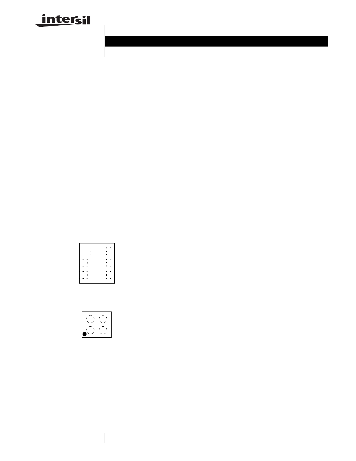
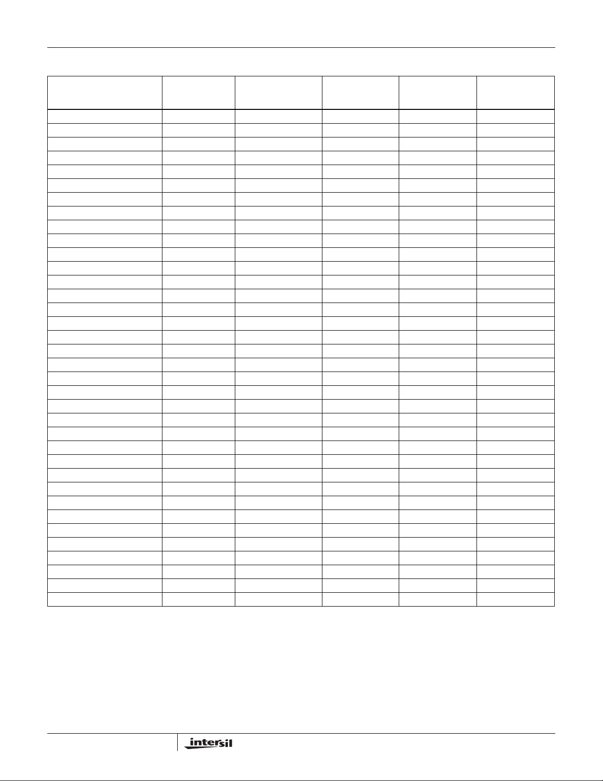
Pinouts
ISL9021
(6 LD 1.6x1.6 µTDFN)
TOP VIEW
FN6867.2
Features
• High Performance LDO with 250mA guaranteed
continuous output current
• Input Voltage Range: 1.5V to 5.5V
• Output Voltage Range: 0.9V to 3.3V
• High PSRR: 75dB @ 10kHz, 50dB @ 1MHz
• Low Quiescent Current: 35µA
• Dropout Voltage: <150mV @ 250mA
• Stable with 1µF to 4.7µF Output Capacitance (±30%) with
an ESR range of 5mΩ to 400mΩ
• ±1.8% Output Accuracy Over-Temperature/Load/Line
• Soft-start Limits Input Current Surge During Enable
• Current Limit and Overheat Protection
• -40°C to +85°C Operating Temp e r at ure Range
• Available in 1.155mmx0.975mm 4-bump WLCSP
Package and 1.6mmx1.6mm 6 Ld µTDFN
• Pb-free (RoHS compliant)
Applications
• PDAs, Cell Phones and Smart Phones
B2
6
5
4
VOUT
VIN
VO
NC
GND
VIN
1
NC
2
EN
3
ISL9021
(4 BALL 1.155x0.975 WLCSP)
TOP VIEW
GND
A2
EN
A1 B1
• Portable Instruments, MP3 Players
• Handheld Devices including Medical Handhelds
1
CAUTION: These devices are sensitive to electrostatic discharge; follow proper IC Handling Procedures.
1-888-INTERSIL or 1-888-468-3774
| Intersil (and design) is a registered trademark of Intersil Americas Inc.
Copyright Intersil Americas Inc. 2009, 2010. All Rights Reserved
All other trademarks mentioned are the property of their respective owners.
ISL9021
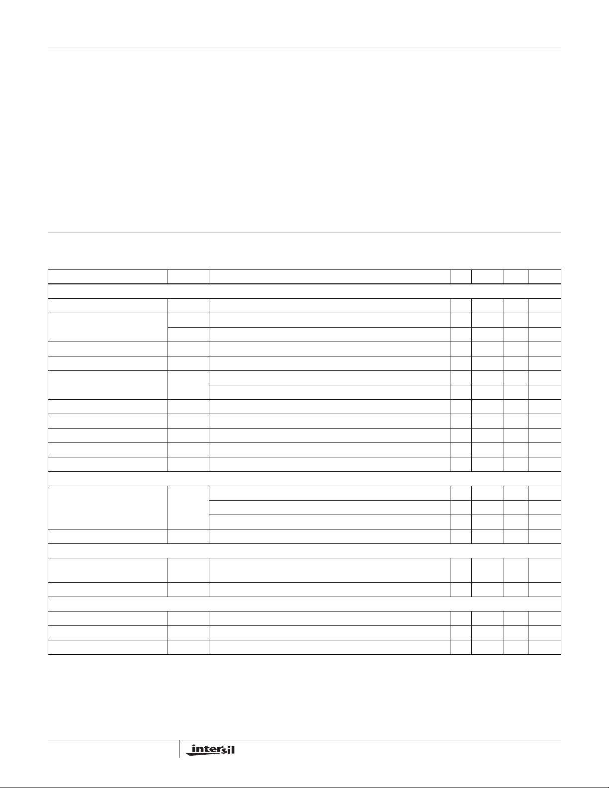
Ordering Information
PACKAGE
PART NUMBER PART
MARKING
ISL9021II1Z-T (Notes 1, 3) 0211 1.1 -40 to +85 4 Ball WLCSP W2x2.4
ISL9021II2Z-T (Notes 1, 3) 0212 2.1 -40 to +85 4 Ball WLCSP W2x2.4
ISL9021II3Z-T (Notes 1, 3) 0213 1.3 -40 to +85 4 Ball WLCSP W2x2.4
ISL9021II4Z-T (Notes 1, 3) 0214 1.0 -40 to +85 4 Ball WLCSP W2x2.4
ISL9021IIBZ-T (Notes 1, 3) 021B 1.5 -40 to +85 4 Ball WLCSP W2x2.4
ISL9021IICZ-T (Notes 1, 3) 021C 1.8 -40 to +85 4 Ball WLCSP W2x2.4
ISL9021IIFZ-T (Notes 1, 3) 021F 2.5 -40 to +85 4 Ball WLCSP W2x2.4
ISL9021IIGZ-T (Notes 1, 3) 021G 2.7 -40 to +85 4 Ball WLCSP W2x2.4
ISL9021IIJZ-T (Notes 1, 3) 021J 2.8 -40 to +85 4 Ball WLCSP W2x2.4
ISL9021IIKZ-T (Notes 1, 3) 021K 2.85 -40 to +85 4 Ball WLCSP W2x2.4
ISL9021IIMZ-T (Notes 1, 3) 021M 3.0 -40 to +85 4 Ball WLCSP W2x2.4
ISL9021IINZ-T (Notes 1, 3) 021N 3.3 -40 to +85 4 Ball WLCSP W2x2.4
ISL9021IIPZ-T (Notes 1, 3) 021P 1.85 -40 to +85 4 Ball WLCSP W2x2.4
ISL9021IIRZ-T (Notes 1, 3) 021R 2.6 -40 to +85 4 Ball WLCSP W2x2.4
ISL9021IISZ-T (Notes 1, 3) 021S 1.6 -40 to +85 4 Ball WLCSP W2x2.4
ISL9021IITZ-T (Notes 1, 3) 021T 1.9 -40 to +85 4 Ball WLCSP W2x2.4
ISL9021IIWZ-T (Notes 1, 3) 021W 1.2 -40 to +85 4 Ball WLCSP W2x2.4
ISL9021IIYZ-T (Notes 1, 3) 021Y 0.9 -40 to +85 4 Ball WLCSP W2x2.4
ISL9021IRU1Z-T (Notes 1, 4) S1 1.1 -40 to +85 6 Ld µTDFN L6.1.6x1.6
ISL9021IRU2Z-T (Notes 1, 4) S9 2.1 -40 to +85 6 Ld µTDFN L6.1.6x1.6
ISL9021IRU3Z-T (Notes 1, 4) S3 1.3 -40 to +85 6 Ld µTDFN L6.1.6x1.6
ISL9021IRU4Z-T (Notes 1, 4) S0 1.0 -40 to +85 6 Ld µTDFN L6.1.6x1.6
ISL9021IRUBZ-T (Notes 1, 4) S4 1.5 -40 to +85 6 Ld µTDFN L6.1.6x1.6
ISL9021IRUCZ-T (Notes 1, 4) S6 1.8 -40 to +85 6 Ld µTDFN L6.1.6x1.6
ISL9021IRUFZ-T (Notes 1, 4) T0 2.5 -40 to +85 6 Ld µTDFN L6.1.6x1.6
ISL9021IRUGZ-T (Notes 1, 4) T2 2.7 -40 to +85 6 Ld µTDFN L6.1.6x1.6
ISL9021IRUJZ-T (Notes 1, 4) T3 2.8 -40 to +85 6 Ld µTDFN L6.1.6x1.6
ISL9021IRUKZ-T (Notes 1, 4) T4 2.85 -40 to +85 6 Ld µTDFN L6.1.6x1.6
ISL9021IRUMZ-T (Notes 1, 4) T5 3.0 -40 to +85 6 Ld µTDFN L6.1.6x1.6
ISL9021IRUNZ-T (Notes 1, 4) R8 3.3 -40 to +85 6 Ld µTDFN L6.1.6x1.6
ISL9021IRUPZ-T (Notes 1, 4) S7 1.85 -40 to +85 6 Ld µTDFN L6.1.6x1.6
ISL9021IRURZ-T (Notes 1, 4) T1 2.6 -40 to +85 6 Ld µTDFN L6.1.6x1.6
ISL9021IRUSZ-T (Notes 1, 4) S5 1.6 -40 to +85 6 Ld µTDFN L6.1.6x1.6
ISL9021IRUTZ-T (Notes 1, 4) S8 1.9 -40 to +85 6 Ld µTDFN L6.1.6x1.6
ISL9021IRUWZ-T (Notes 1, 4) S2 1.2 -40 to +85 6 Ld µTDFN L6.1.6x1.6
ISL9021IRUYZ-T (Notes 1, 4) R9 0.9 -40 to +85 6 Ld µTDFN L6.1.6x1.6
NOTES:
1. Please refer to TB347 for details on reel specifications.
2. For other output voltages, contact Intersil Marketing.
3. These Intersil Pb-free WLCSP and BGA packaged products employ special Pb-free material sets; molding compounds/die attach materials and
SnAgCu - e1 solder ball terminals, which are RoHS compliant and compatible with both SnPb and Pb-free soldering operations. Intersil Pb-free
WLCSP and BGA packaged products are MSL classified at Pb-free peak reflow temperatures that meet or exceed the Pb-free requirements of
IPC/JEDEC J STD-020.
4. These Intersil Pb-free plastic packaged products employ special Pb-free material sets; molding compounds/die attach materials and NiPdAu
plate - e4 termination finish, which is RoHS compliant and compatible with both SnPb and Pb-free soldering operations. Intersil Pb-free products
are MSL classified at Pb-free peak reflow temperatures that meet or exceed the Pb-free requirements of IPC/JEDEC J STD-020.
VO Voltage
(Note 2)
TEMP RANGE
(°C)
Tape & Reel
(Pb-free)
PACKAGE
DWG. #
2
FN6867.2
January 14, 2010
ISL9021
Absolute Maximum Ratings Thermal Information
Supply Voltage (VIN) . . . . . . . . . . . . . . . . . . . . . . . . . . . . . . . . +6.5V
All Other Pins . . . . . . . . . . . . . . . . . . . . . . . . . . -0.3 to (VIN + 0.3)V
Thermal Resistance (Typical, Note 5) θ
4 Ball WLCSP . . . . . . . . . . . . . . . . . . . . . . . . . . . . . 135.64
6 Lead µTDFN . . . . . . . . . . . . . . . . . . . . . . . . . . . . . 140
Recommended Operating Conditions
Ambient Temperature Range (TA) . . . . . . . . . . . . . . .-40°C to +85°C
Supply Voltage (V
) . . . . . . . . . . . . . . . . . . . . . . . . . . . . 1.5 to 5.5V
IN
Junction Temperature Range . . . . . . . . . . . . . . . . .-40°C to +125°C
Operating Temperature Range . . . . . . . . . . . . . . . . .-40°C to +85°C
Storage Temperature Range . . . . . . . . . . . . . . . . . .-65°C to +150°C
Pb-Free Reflow Profile. . . . . . . . . . . . . . . . . . . . . . . . .see link below
http://www.intersil.com/pbfree/Pb-FreeReflow.asp
CAUTION: Do not operate at or near the maximum ratings listed for extended periods of time. Exposure to such conditions may adversely impact product reliability and
result in failures not covered by warranty.
NOTE:
is measured in free air with the component mounted on a high effective thermal conductivity test board with “direct attach” features. See
5. θ
JA
Tech Brief TB379.
(°C/W)
JA
Electrical Specifications T
= -40°C to +85°C; V
A
with MIN and/or MAX limits are 100% tested at +25°C, unless otherwise specified. Temperature limits
= (VO + 0.5V) to 5.5V with a minimum VIN of 1.5V; C
IN
= 1µF; CO = 1µF; Parameters
IN
established by characterization and are not production tested.
PARAMETER SYMBOL TEST CONDITIONS MIN TYP MAX UNIT
DC CHARACTERISTICS
Supply Voltage V
Undervoltage Lockout
V
IN
Threshold
Ground Current I
Shutdown Current I
IN
V
UVLO+VIN
V
UVLO-VIN
DD
DDS
Output Voltage Accuracy V
Maximum Output Current I
Internal Current Limit I
Dropout Voltage (Notes 6, 7) V
Thermal Shutdown Temperature T
MAX
LIM
DOIO
SD
Rising 1.425 1.5 V
Falling 1.3 1.375 V
Output Enabled; IO = 0; V
V
= 5.5V, EN = Low, IO = 0 0.1 1.0 µA
IN
= VO + 0.5V to 5.5V, IO = 1mA to 150mA, TJ = +25°C -0.8 +0.8 %
IN
= VO + 0.5V to 5.5V , IO = 1mA to 150mA, TJ = -40°C to +125°C -1.8 +1.8
V
IN
= 1.5V to 5.5V 35 50 µA
IN
Continuous 250 mA
260 mA
= 250mA; VO > 1.8V 150 250 mV
1.5 5.5 V
160 °C
Thermal Shutdown Hysteresis 20 °C
AC CHARACTERISTICS
Ripple Rejection (Note 6) V
Output Noise Voltage (Note 6) V
= 4.5V, VO = 3.3V @ 1kHz 60 dB
IN
V
= 4.5V, VO = 3.3V @ 10kHz 75 dB
IN
V
= 4.5V, VO = 3.3V @ 1MHz 50 dB
IN
= 4.2V, TA = +25°C, BW = 10Hz to 100kHz, IO = 10mA 8.5*V
IN
O
µV
DEVICE START-UP CHARACTERISTICS
Device Enable Time t
LDO Soft-start Ramp Rate t
SSR
Time from assertion of the EN pin to when the output voltage
EN
reaches 95% of the V
(nom)
O
250 600 µs
Slope of linear portion of LDO output voltage ramp during start-up 30 60 µs/V
EN LOGIC CHARACTERISTICS
Input Low Voltage V
Input High Voltage V
Input Leakage Current I
IL, IIH
IL
IH
1.1 V
0.4 V
0.1 µA
NOTES:
6. Limits established by characterization and are not production tested.
7. Dropout voltage is measured as V
- VO, when VO is 4% lower than the value of VO; when VIN = VO + 0.5V.
IN
RMS
3
FN6867.2
January 14, 2010

Typical Operating Performance
45
T = ROOM TEMP
40
35
30
25
20
15
T = -40°C
10
QUIESCENT CURRENT (µA)
5
0
1.52.53.54.55.5
T = +45°C
T = -25°C
INPUT VOLTAGE (V)
FIGURE 1. QUIESCENT CURRENT vs INPUT VOLTAGE
(V
= 0.9V)
OUT
T = +85°C
T = 0°C
ISL9021
45
T = ROOM TEMP
40
35
30
25
20
15
10
QUIESCENT CURRENT (µA)
T = -40°C
5
0
1.5 2.5 3.5 4.5 5.5
T = +45°C
T = -25°C
INPUT VOLTAGE (V)
T = +85°C
T = 0°C
FIGURE 2. QUIESCENT CURRENT vs INPUT VOLTAGE
(V
= 1.85V)
OUT
50
T = ROOM TEMP
40
30
20
T = -40°C
10
0
QUIESCENT CURRENT (µA)
-10
3.5 4.0 4.5 5.0 5.5 6.0
T = -25°C
INPUT VOLTAGE (V)
T = +45°C
T = +85°C
T = 0°C
FIGURE 3. QUIESCENT CURRENT vs INPUT VOLTAGE
= 3.3V)
(V
OUT
2.00
1.95
1.90
1.85
1.80
1.75
Vo (V)
1.70
1.65
1.60
1.55
1.50
+25°C
+85°C
2.53.54.55.56.5
-40°C
V
(V)
IN
FIGURE 5. LINE REGULA TION vs TEMPERA TU RE
= 1.85V)
(V
OUT
1.95
1.90
1.85
1.80
Vo (V)
1.75
1.70
1.65
1.60
+85°C
0 50 100 150 200 250 300
+25°C
-40°C
Io (mA)
FIGURE 4. LOAD REGULA TION vs TEMPERA T URE
(V
=1.85V)
OUT
3.5
3.4
+25°C
3.3
3.2
Vo (V)
3.1
3.0
2.9
2.8
0 50 100 150 200 250 300
-40°C
Io (mA)
+85°C
FIGURE 6. LOAD REGULA TION vs TEMPERA T URE
=3.3V)
(V
OUT
4
FN6867.2
January 14, 2010

Typical Operating Performance (Continued)
3.50
3.45
3.40
3.35
3.30
3.25
Vo (V)
3.20
3.15
3.10
3.05
3.00
FIGURE 7. LINE REGULA TION vs TEMPERA TU RE
+25°C
-40°C
3.5 4.0 4.5 5.0 5.5 6.0
(V)
V
IN
(V
=3.3V)
OUT
+85°C
ISL9021
1.05
1.00
+25°C
0.95
0.90
0.85
0.80
Vo (V)
0.75
0.70
0.65
0.60
0 50 100 150 200 250 300
-40°C
Io (mA)
+85°C
FIGURE 8. LOAD REGULA TION vs TEMPERA T URE
(V
=0.9V)
OUT
1.00
0.95
0.90
0.85
Vo (V)
0.80
0.75
0.70
+25°C
-40°C
3.0 3.5 4.0 4.5 5.0 5.5 6.0
(V)
V
IN
+85°C
FIGURE 9. LINE REGULA TION vs TEMPERA TU RE
=0.9V)
(V
OUT
VIN = 2.7V
= 4.7µF
C
OUT
V
OUT
V
= 1.85V
OUT
V
= 1.85V
OUT
V
OUT
I
OUT
I
= 1mA TO 250mA
OUT
FIGURE 10. LOAD TRANSIENT RESPONSE
VIN = 2.7V
C
= 1µF
OUT
I
OUT
I
= 1mA TO 250mA
OUT
FIGURE 11. LOAD TRANSIENT RESPONSE
5
FIGURE 12. ENABLE FUNCTION (V
C
1µF)
OUT
= 3.6V , V
IN
= 1.85V ,
OUT
January 14, 2010
FN6867.2

ISL9021
Typical Operating Performance (Continued)
-20
VIN = 4.5VDC + 50mVAC
-30
C
= 1µF
OUT
-40
-50
-60
PSRR (dB)
-70
-80
-90
100 1k 10k 100k 1M
IO = 10mA
IO = 0A
FREQUENCY (Hz)
FIGURE 13. POWER SUPPLY REJECTION vs FREQUENCY
Pin Descriptions
PIN
NAME DESCRIPTION
VIN IC Supply/LDO Input. Connect a 1µF capacitor to GND.
GND System ground pin.
EN LDO Enable. When this signal goes high, the LDO is turned on.
VO LDO Output. Connect a 1µF to 4.7µF capacitor to GND.
E-Pad For µTDFN package option only. Connect it to the system ground.
Typical Application
VIN (1.5V TO 5.5V)
ENABLE
OFF
ON
ISL9021
VIN
EN
C1 C2
VO
GND
VOUT
C1, C2: 1µF X5R CERAMIC CAPACITOR
6
FN6867.2
January 14, 2010

Block Diagram
ISL9021
VIN
EN
TEMP
SENSOR
CONTROL
LOGIC
VOLTAGE
AND
REFERENCE
GENERATOR
BANDGAP
PASS ELEMENT
SHORT-CIRCUIT
PROTECTION
THERMAL PROTECTION
SOFT-START
+
VOUT
GND
7
FN6867.2
January 14, 2010

ISL9021
Functional Description
The ISL9021 is a high performance low-dropout regulator
(LDO) with 250mA sourcing capability. The extra low ground
current makes this part a good choice for handheld product
applications. The device also incorporates overcurrent,
thermal shutdown, reverse current protections, and soft-start
features.
Thermal shutdown protects the device against overheating.
Soft-start limits the start-up input current surges. In some
applications, the output voltage may be externally pulled
higher than input, or the input voltage could be connected to
ground, or connected to some voltage lower than the output
side. The ISL9021 features reverse current protection; that
can block the reverse current from output to input.
Enable Control
The ISL9021 has an enable pin. When EN is low, the IC is in
shutdown mode. In this condition, all on-chip circuits are off,
and the device draws minimum current, typically less than
0.1µA(typ). Driving this pin high will turn on the device.
LDO Protections
The ISL9021 offers several protection functions, making it ideal
for use in battery-powered applications.The ISL9021 provides
short-circuit protection by limiting the output current at current
limit of 260mA(min). If the short circuit lasts long enough, the
die temperature increases, and the over-temperature protection
circuit will shut down the output. When the die temperature
reaches about +145°C, thermal protection starts to work with
output being loaded with at least 50mA. Once the die
temperature drops to about +1 10°C, the LDO will resume
operation beginning with a soft-start.
The ISL9021’s reverse current protection is intended to
block reverse conduction if output voltage is higher than
input voltage.
Input and Output Capacitors
The ISL9021 provides a linear regulator that has low
quiescent current, fast transient response, and overall stable
operation across the recommended operating conditions. A
ceramic capacitor (X5R or X7R) with a capacitance of 1µF to
4.7µF with an ESR up to 400mΩ is suitable for the ISL9021
to maintain its output stability. The ground connection of the
output capacitor should be routed directly to the GND pin of
the device, and also placed close to the IC. Similarly for the
input capacitor, usually a 1µF ceramic capacitor (X5R or 7R)
is suitable for most cases, but if a large, fast rising load
transient condition is expected, a higher value input
capacitor may be necessary to achieve satisfactory
performance.
Board Layout Recommendations
A good PCB layout is an important step to achieve good
performance. It is recommended to design the board with
separate ground planes for input and output, and connect
both ground planes at the GND pin of the IC. Consideration
should be taken when placing the components and routing
the trace to minimize the ground impedance, and keep the
parasitic inductance low. Usually the input/output capacitors
should be placed as close to the IC as possible with a good
ground connection.
8
FN6867.2
January 14, 2010

ISL9021
Wafer Level Chip Scale Package
(WLCSP 0.4mm Ball Pitch)
D
E
PIN 1
TOP VIEW
A2
A1
b
SIDE VIEW
W2x2.4
2x2 ARRAY 4 BALL WAFER LEVEL CHIP SCALE PACKAGE
SYMBOL MILLIMETERS
A 0.44 Min, 0.495 Nom, 0.55 Max
A1 0.190 ±0.030
A2 0.305 ±0.025
b 0.270 ±0.030
D 1.155 ±0.020
D1 0.400 BASIC
E 0.975 ±0.020
E1 0.400 BASIC
e 0.400 BASIC
SD 0.200 BASIC
SE 0.00 BASIC
NUMBER OF BUMPS: 4
Rev. 2 6/08
A
NOTES:
1. All dimensions are in millimeters.
e ( D1 )
2
SE
b
SD
BOTTOM VIEW
e ( E1 )
1
AB
All Intersil U.S. products are manufactured, assembled and tested utilizing ISO9000 quality systems.
Intersil Corporation’s quality certifications can be viewed at www.intersil.com/design/quality
Intersil products are sold by description only. Intersil Corporation reserves the right to make changes in circuit design, software and/or specifications at any time without
notice. Accordingly, the reader is cautioned to verify that data sheets are current before placing orders. Information furnished by Intersil is believed to be accurate and
reliable. However, no responsibility is assumed by Intersil or its subsidiaries for its use; nor for any infringements of patents or other rights of third parties which may result
from its use. No license is granted by implicat ion or oth erwise u nde r any p a tent or p at ent r ights of Intersil or its subsidiaries.
For information regarding Intersil Corporation and its products, see www.intersil.com
9
FN6867.2
January 14, 2010

ISL9021
Package Outline Drawing
L6.1.6x1.6
6 LEAD ULTRA THIN DUAL FLAT NO-LEAD COL PLASTIC PACKAGE (UTDFN COL)
Rev 1, 11/07
(4X)
( 1 . 4 )
0.15
6
PIN 1
INDEX AREA
TOP VIEW
1.60
A
B
1.60
( 6X 0 . 25 )
( 1X 0 .70 )
PIN #1 INDEX AREA
6
1X 0.5 ±0.1
0 . 55 MAX
2X 1.00
0.50
4X
1
6
BOTTOM VIEW
SIDE VIEW
3
5X 0 . 40 ± 0 . 1
4
0.104CAMB
0.25 +0.05 / -0.07
SEE DETAIL "X"
BASE PLANE
C
0.10
C
SEATING PLANE
0.08
C
( 4X 0 . 5 )
TYPICAL RECOMMENDED LAND PATTERN
10
( 5X 0 . 60 )
C
0 . 2 REF
0 . 00 MIN.
0 . 05 MAX.
DETAIL "X"
NOTES:
Dimensions are in millimeters.1.
Dimensions in ( ) for Reference Only.
2.
Dimensioning and tolerancing conform to AMSE Y14.5m-1994.
3.
Unless otherwise specified, tolerance : Decimal ± 0.05
4.
Dimension b applies to the metallized terminal and is measured
between 0.15mm and 0.30mm from the terminal tip.
Tiebar shown (if present) is a non-functional feature.
5.
The configuration of the pin #1 identifier is optional, but must be
6.
located within the zone indicated. The pin #1 identifier may be
either a mold or mark feature.
FN6867.2
January 14, 2010
 Loading...