

Page 1
®
ISL9016
FN6832.0Data Sheet January 22, 2009
150mA Dual LDO with Low Noise, High
PSRR, and Low I
ISL9016 is a high performance dual LDO capable o f providing
up to 150mA current on each channel. It features a low
standby current and very high PSRR and is sta ble with output
capacitance of 1µF to 4.7µF with an ESR of up to 200mΩ.
The device integrates a separate enable function for each
output. The quiescent current is typically 49µA when only
one LDO is enabled and typically 80µA when both LDOs are
enabled. When both LDOs are under shutdown condition,
the drawing current is typically less than 1µA.
ISL9016 provides a wide input voltage range from 1.8V to
6.5V. It also has a high PSRR of 80dB at 1kHz and 45dB at
1MHz. ISL9016 also provides output current limit, overheat
protection, reverse current protection, as well as excellent
load transient response.
ISL9016 is offered in a tiny 1.6mmx1.6mm 6 Ld µTDFN
package. Output voltage options are available from 1.2V to
3.3V. Several combinations of voltage outputs are standard
and others may be available upon request.
Q
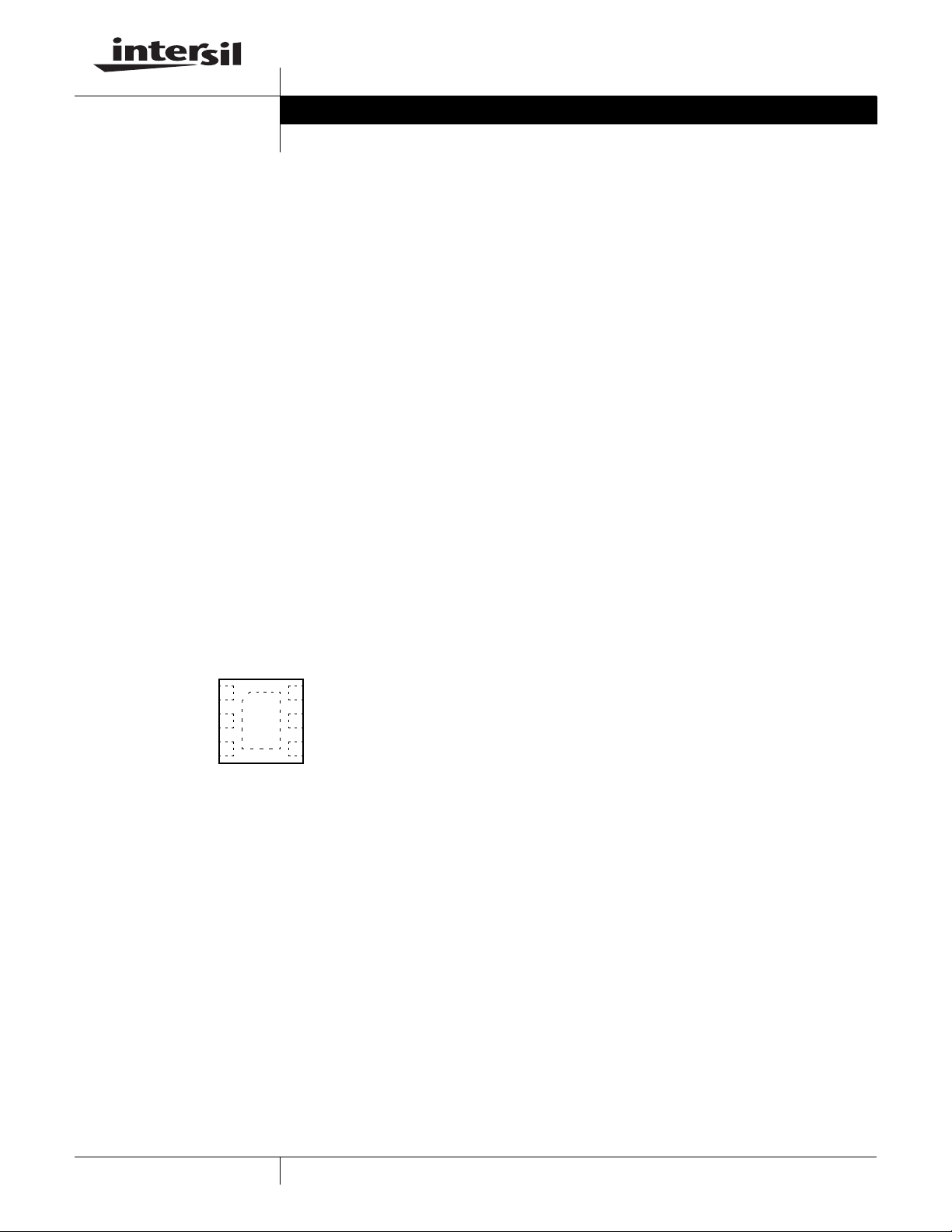
Pinout
ISL9016
(6 LD 1.6x1.6 µTDFN)
TOP VIEW
VIN
GND
1
2
6
5
VOUT1
VOUT2
Features
• Dual Integrated 150mA High Performance LDOs
• High PSRR: 80dB @ 1kHz and 45dB @ 1MHz
• Reverse Current Protection
• Low Quiescent Current
- 49µA (Single LDO Enabled)/80µA (Dual LDOs Enabled)
• Excellent Load Transient Response
• Typically ±0.8% Output Voltage Accuracy
• Low Output Noise: Typically 25µV
RMS
• Wide Input Voltage Capability: 1.8V to 6.5V
• Low Dropout Voltage: Typically 120mV @ 150mA
• Separate Enable Control for each LDO
• Stable with 1µF to 4.7µF Ceramic Output Capacitors
• Soft-start to Limit Input Current Surge During Enable
• Current Limit and Overheat Protection
• Tiny 6 Ld 1.6mmx1.6mm µTDFN package
• Pb-free (RoHS Compliant)
Applications
• PDAs, Cell Phones and Smart Phones
• Portable Instruments, MP3/4 Players, PMP, DSC
• Handheld Devices including Medical Handhelds
EN2
3
1
EN1
4
CAUTION: These devices are sensitive to electrostatic discharge; follow proper IC Handling Procedures.
1-888-INTERSIL or 1-888-468-3774
| Intersil (and design) is a registered trademark of Intersil Americas Inc.
All other trademarks mentioned are the property of their respective owners.
Copyright © Intersil Americas Inc. 2009. All Rights Reserved.
Page 2
Ordering Information
ISL9016
PART NUMBER
(Notes 1, 3) PART MARKING
ISL9016IRUWCZ-T N7 1.2 1.8 -40 to +85 6 Ld µTDFN L6.1.6x1.6A
ISL9016IRUWGZ-T N6 1.2 2.7 -40 to +85 6 Ld µTDFN L6.1.6x1.6A
ISL9016IRUWJZ-T N2 1.2 2.8 -40 to +85 6 Ld µTDFN L6.1.6x1.6A
ISL9016IRUWKZ-T N1 1.2 2.85 -40 to +85 6 Ld µTDFN L6.1.6x1.6A
ISL9016IRUBWZ-T R7 1.5 1.2 -40 to +85 6 Ld µTDFN L6.1.6x1.6A
ISL9016IRUBBZ-T R6 1.5 1.5 -40 to +85 6 Ld µTDFN L6.1.6x1.6A
ISL9016IRUCWZ-T R5 1.8 1.2 -40 to +85 6 Ld µTDFN L6.1.6x1.6A
ISL9016IRUCBZ-T R4 1.8 1.5 -40 to +85 6 Ld µTDFN L6.1.6x1.6A
ISL9016IRUFWZ-T R3 2.5 1.2 -40 to +85 6 Ld µTDFN L6.1.6x1.6A
ISL9016IRUFBZ-T N8 2.5 1.5 -40 to +85 6 Ld µTDFN L6.1.6x1.6A
ISL9016IRUFCZ-T N9 2.5 1.8 -40 to +85 6 Ld µTDFN L6.1.6x1.6A
ISL9016IRUFFZ-T P0 2.5 2.5 -40 to +85 6 Ld µTDFN L6.1.6x1.6A
ISL9016IRUGWZ-T P1 2.7 1.2 -40 to +85 6 Ld µTDFN L6.1.6x1.6A
ISL9016IRUGCZ-T R2 2.7 1.8 -40 to +85 6 Ld µTDFN L6.1.6x1.6A
ISL9016IRUGGZ-T N3 2.7 2.7 -40 to +85 6 Ld µTDFN L6.1.6x1.6A
ISL9016IRUJWZ-T P2 2.8 1.2 -40 to +85 6 Ld µTDFN L6.1.6x1.6A
ISL9016IRUJBZ-T P3 2.8 1.5 -40 to +85 6 Ld µTDFN L6.1.6x1.6A
ISL9016IRUJCZ-T N4 2.8 1.8 -40 to +85 6 Ld µTDFN L6.1.6x1.6A
ISL9016IRUJJZ-T N0 2.8 2.8 -40 to +85 6 Ld µTDFN L6.1.6x1.6A
ISL9016IRUKWZ-T P5 2.85 1.2 -40 to +85 6 Ld µTDFN L6.1.6x1.6A
ISL9016IRUKFZ-T P4 2.85 2.5 -40 to +85 6 Ld µTDFN L6.1.6x1.6A
ISL9016IRUKKZ-T N5 2.85 2.85 -40 to +85 6 Ld µTDFN L6.1.6x1.6A
ISL9016IRUMWZ-T P6 3.0 1.2 -40 to +85 6 Ld µTDFN L6.1.6x1.6A
ISL9016IRUMBZ-T P7 3.0 1.5 -40 to +85 6 Ld µTDFN L6.1.6x1.6A
ISL9016IRUMCZ-T P8 3.0 1.8 -40 to +85 6 Ld µTDFN L6.1.6x1.6A
ISL9016IRUMKZ-T P9 3.0 2.85 -40 to +85 6 Ld µTDFN L6.1.6x1.6A
ISL9016IRUNWZ-T R0 3.3 1.2 -40 to +85 6 Ld µTDFN L6.1.6x1.6A
ISL9016IRUNCZ-T R1 3.3 1.8 -40 to +85 6 Ld µTDFN L6.1.6x1.6A
NOTES:
1. Please refer to TB347 for details on reel specifications.
2. For other output voltages, contact Intersil marketing or local sales office.
3. These Intersil Pb-free plastic packaged products employ special Pb-free material sets; molding compounds/die attach materials and NiPdAu plate - e4
termination finish, which is RoHS compliant and compatible with both SnPb and Pb-free soldering operations. Intersil Pb-free products are MSL
classified at Pb-free peak reflow tempera tures th at meet or exceed the Pb-free re quiremen ts of IPC/JEDEC J ST D-020.
VO1 VOLTAGE
(V) (Note 2)
VO2 VOLTAGE
(V) (Note 2)
TEMP RANGE
(°C)
PACKAGE
(Pb-Free)
PKG
DWG. #
2
FN6832.0
January 22, 2009
Page 3
ISL9016
Absolute Maximum Ratings Thermal Information
VIN to GND . . . . . . . . . . . . . . . . . . . . . . . . . . . . . . . . -0.3V to +7.1V
All Other Pins to GND . . . . . . . . . . . . . . . . . . . . -0.3 to (V
+0.3)V
IN
Recommended Operating Conditions
Supply Voltage (VIN) . . . . . . . . . . . . . . . . . . . . . . . . . . .1.8V to 6.5V
Each LDO Load Current . . . . . . . . . . . . . . . . . . . . . . . .up to 150mA
Ambient Temperature Range (T
CAUTION: Do not operate at or near the maximum ratings listed for extended periods of time. Exposure to such conditions may adversely impact product reliability and
result in failures not covered by warranty.
) . . . . . . . . . . . . . . .-40°C to +85°C
A
NOTE:
is measured in free air with the component mounted on a high effective thermal conductivity test board with “direct attach” features. See
4. θ
JA
Tech Brief TB379.
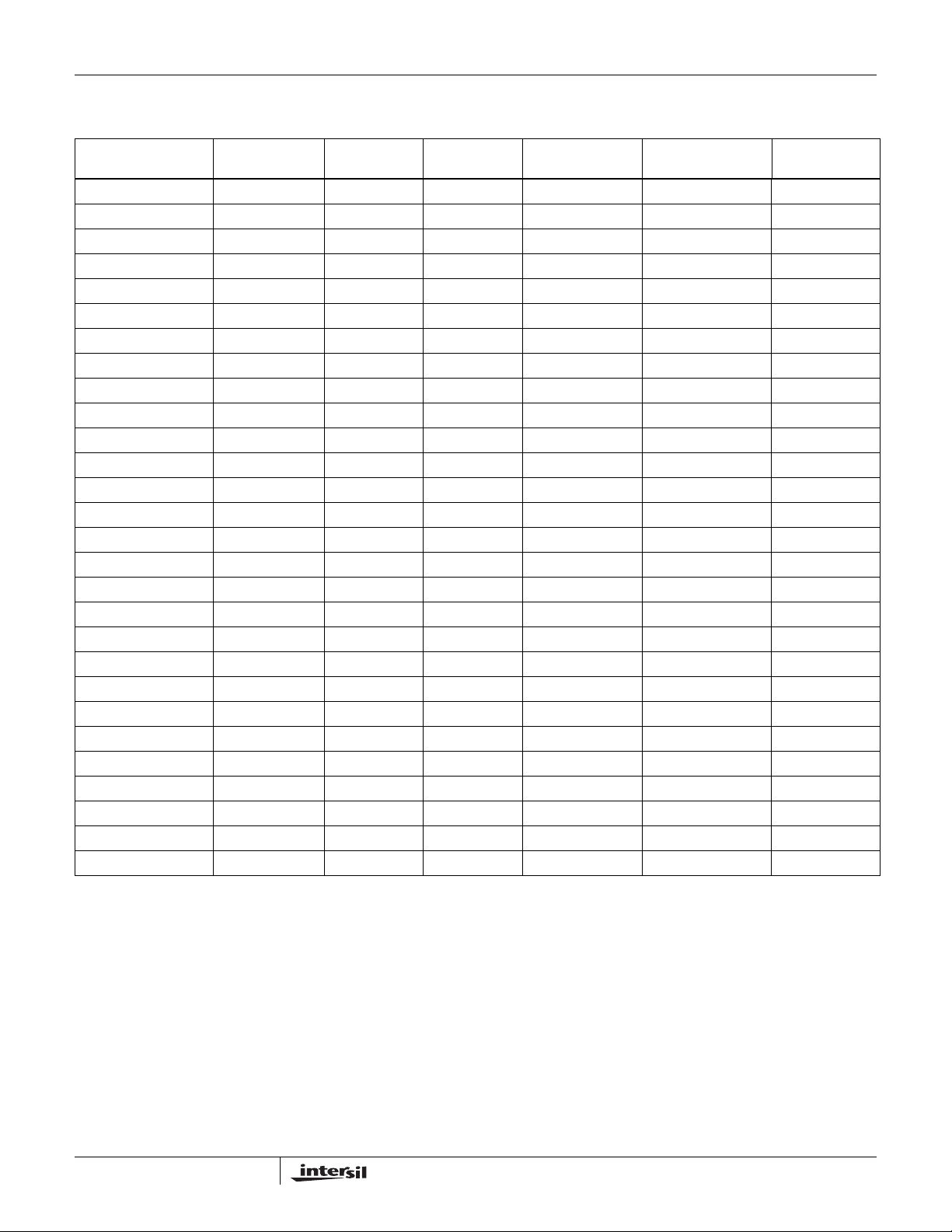
Electrical Specifications Unless otherwise noted, all parameter limits are guaranteed over the recommended operating conditions and
the typical specifications are measured at the following conditions: T
a minimum V
+25°C, unless otherwise specified. Temperature limits established by characterization and are not production
tested.
PARAMETER SYMBOL TEST CONDITIONS MIN TYP MAX UNITS
DC CHARACTERISTICS
Supply Voltage V
UVLO Threshold V
V
IN
UV+
UV-
Input Quiescent Current Quiescent condition: I
I
DD1
I
DD2
Shutdown Current I
DDS
Regulation Voltage Accuracy V
Maximum Output Current I
Internal Current Limit I
Dropout Voltage (Note 5) V
Thermal Shutdown Temperature T
MAX
LIM
DO1IO
V
DO2IO
V
DO3IO
SD+
T
SD-
AC CHARACTERISTICS
Ripple Rejection I
Output Noise Voltage V
DEVICE START-UP CHARACTERISTICS
Device Enable Time t
EN
of 1.8V; CIN = 1µF; CO = 1µF. Parameters with MIN and/or MAX limits are 100% tested at
IN
O1
One LDO active 49 67 µA
Both LDO active 80 100 µA
@ +25°C 0.1 1.0 µA
= VO+ 0.5V to 6.5V, IO = 10µA to 150mA, TA = +25°C -0.8 +0.8 %
IN
V
= VO+ 0.5V to 6.5V, IO = 10µA to 150mA, TA = -40°C to
IN
+85°C
Each LDO, Continuous 150 mA
= 150mA; 1.2V ≤ VO ≤ 2.1V 250 425 mV
= 150mA; 2.1V ≤ VO ≤ 2.8V 200 325 mV
= 150mA; 2.8V ≤ V
= 10mA, VIN = 3.7V(min), VO = 2.7V, TA = +25°C
O
O
@ 1kHz 80 dB
@ 10kHz 60 dB
@ 100kHz 50 dB
@ 1MHz 45 dB
= 4.2V, IO = 10mA, TA = +25°C, BW = 10Hz to 100kHz 25 µV
IN
Time from assertion of the ENx pin to when the output voltage
reaches 95% of the V
O
Thermal Resistance θ
6 Ld μTDFN Package (Note 4). . . . . . . . . . . . . . . 117.5
Junction Temperature Range . . . . . . . . . . . . . . . . .-40°C to +125°C
Operating Temperature Range . . . . . . . . . . . . . . . . .-40°C to +85°C
Storage Temperature Range . . . . . . . . . . . . . . . . . .-65°C to +150°C
Pb-Free Reflow Profile. . . . . . . . . . . . . . . . . . . . . . . . .see link below
http://www.intersil.com/pbfree/Pb-FreeReflow.asp
= +25°C; VIN = (VO+ 0.5V) to 6.5V with
A
1.8 6.5 V
1.710 1.775 V
1.55 1.62
= 0µA; IO2 = 0µA
-1.8 +1.8 %
175 265 355 mA
120 200 mV
145 °C
110 °C
400 600 µs
(nom)
(°C/W)
JA
RMS
3
FN6832.0
January 22, 2009
Page 4
ISL9016
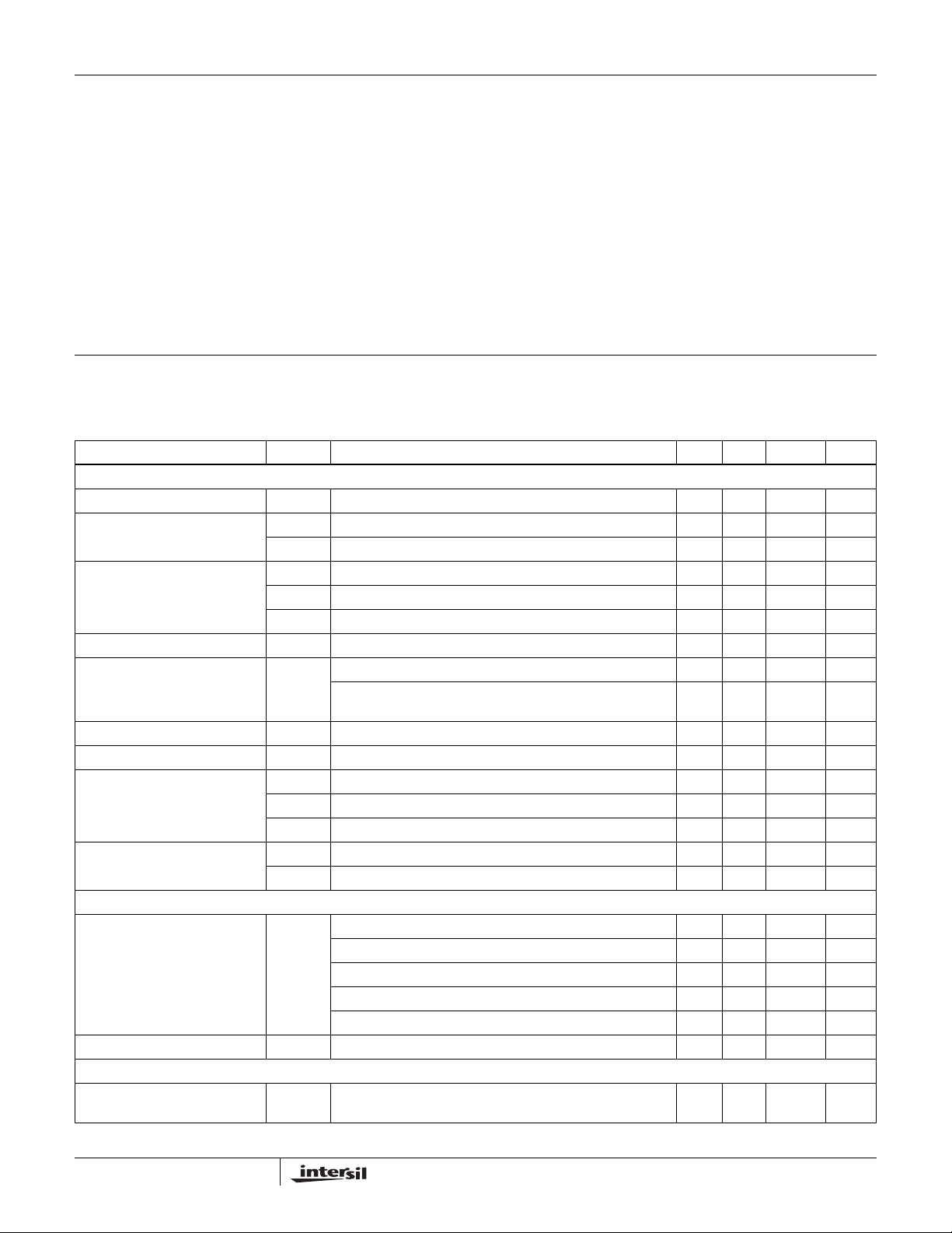
Electrical Specifications Unless otherwise noted, all parameter limits are guaranteed over the recommended operating conditions and
the typical specifications are measured at the following conditions: T
a minimum V
of 1.8V; CIN = 1µF; CO = 1µF. Parameters with MIN and/or MAX limits are 100% tested at
IN
+25°C, unless otherwise specified. Temperature limits established by characterization and are not production
tested. (Continued)
PARAMETER SYMBOL TEST CONDITIONS MIN TYP MAX UNITS
LDO Soft-Start Ramp Rate t
SSR
Slope of linear portion of LDO output voltage ramp during
start-up
EN PIN CHARACTERISTICS
Input Low Voltage V
Input High Voltage V
Input Leakage Current I
IL
TA = -20°C to +85° -0.3 0.4 V
IL
IH
, I
IH
REVERSE CURRENT CHARACTERISTICS
Output Reverse Leakage Current
I
ORLCVIN
= 0V, V
= 5.5V 8 15 µA
OUT
(Note 6)
NOTES:
x = 0.98*VOx(NOM); Valid for VOx greater than 1.80V.
5. V
O
6. Output reverse leakage current is measured with VIN pin grounded and VOUT pin connected to 5.5V.
= +25°C; VIN = (VO+ 0.5V) to 6.5V with
A
30 60 µs/V
1.1 V
+ 0.3 V
IN
0.1 µA
4
FN6832.0
January 22, 2009
Page 5

Typical Operating Performance
ISL9016
55
50
45
40
35
QUIESCENT CURRENT (µA)
30
2.4 3.6 4.8 6.0
T = +25°C
T = -40°C
T = +50°C
T = -25°C
INPUT VOLTAGE (V)
T = +85°C
T = 0°C
FIGURE 1. QUIESCENT CURRENT vs INPUT VOLTAGE
(V
= 2.1V, ONLY LDO1 ENABLED)
OUT1
85
80
75
T = +25°C
T = +50°C
T = +85°C
55
50
45
40
35
QUIESCENT CURRENT (µA)
30
2.4 3.6 4.8 6.0
T = +25°C
T = -40°C
INPUT VOLTAGE (V)
T = +50°C
T = -25°C
T = +85°C
T = 0°C
FIGURE 2. QUIESCENT CURRENT vs INPUT VOLTAGE
(V
= 2.1V, ONLY LDO2 ENABLED)
OUT2
55
T = +25°C
50
45
T = +50°C
T = +85°C
70
65
QUIESCENT CURRENT (µA)
60
2.4 3.6 4.8 6.0
T = -40°C
T = -25°C
INPUT VOLTAGE (V)
T = 0°C
FIGURE 3. QUIESCENT CURRENT vs INPUT VOLTAGE
(V
= V
OUT1
ENABLED)
55
50
45
40
35
QUIESCENT CURRENT (µA)
30
3.6 4.4 5.2 6.0
T = -40°C
= 2.1V, LDO1 AND LDO2
OUT2
T = +25°C
INPUT VOLTAGE (V)
T = +50°C
T = -25°C
T = +85°C
T = 0°C
FIGURE 5. QUIESCENT CURRENT vs INPUT VOLTAGE
(V
= 3.3V, ONLY LDO2 ENABLED)
OUT2
40
35
QUIESCENT CURRENT (µA)
30
3.6 4.4 5.2 6.0
T = -40°C
T = -25°C
INPUT VOLTAGE (V)
T = 0°C
FIGURE 4. QUIESCENT CURRENT vs INPUT VOLTAGE
(V
= 3.3V, ONLY LDO1 ENABLED)
OUT1
85
80
75
70
65
QUIESCENT CURRENT (µA)
60
3.6 4.4 5.2 6.0
T = +25°C
T = +85°C
T = +50°C
T = 0°C
T = -25°C
T = -40°C
INPUT VOLTAGE (V)
FIGURE 6. QUIESCENT CURRENT vs INPUT VOLTAGE
(V
= V
OUT1
ENABLED)
= 3.3V, LDO1 AND LDO2
OUT2
5
FN6832.0
January 22, 2009
Page 6

Typical Operating Performance
15
10
T = +85°C
ISL9016
10
5
T = +85°C
T = +25°C
5
0
(mV)
O
ΔV
-5
-10
-15
1.5 3.0 4.5 6.0
FIGURE 7. ΔV
1.22
1.21
1.20
1.19
OUTPUT VOLTAGE (V)
1.18
0 30 60 90 120 150
OUT
(V
OUT_NOMINAL
T = -40°C
FIGURE 9. LOAD REGULATION (V
T = +25°C
INPUT VOLTAGE (V)
vs INPUT VOL T AGE
= 1.2V, I
T = +85°C
T = +25°C
LOAD CURRENT (mA)
T = -40°C
OUT
= 1.8V, V
IN
= 50mA)
OUT
0
-5
(mV)
O
ΔV
-10
-15
-20
1.5 2.5 3.5 4.5 5.5
FIGURE 8. ΔV
3.32
3.31
3.30
3.29
3.28
3.27
OUTPUT VOLTAGE (V)
3.26
3.25
0 30 60 90 120 150
vs INPUT VOLT AGE
OUT
(V
OUT_NOMINAL
T = -40°C
INPUT VOLTAGE (V)
= 1.2V, I
T = +25°C
T = -40°C
LOAD CURRENT (mA)
= 1.2V) FIGURE 10. LOAD REGULATION (V
OUT
= 4.5V, V
IN
= 150mA)
T = +85°C
OUT
= 3.3V)
5V/DIV
1V/DIV
1V/DIV
V
V
EN1 = EN2
OUT1
OUT2
FIGURE 11. ENABLE OPERATION (V
V
OUT1
= V
OUT1
= 1.2V)
6
= 3.6V ,
IN
100µs/DIV
V
5V/DIV
50mV/DIV
50mV/DIV
200mA/DIV
IN
V
OUT1
V
(AC COUPLED)
OUT2
I
OUT1
(AC COUPLED)
FIGURE 12. LOAD TRANSIENT RESPONSE (V
V
OUT1
= V
OUT2
= 1.2V, I
0.01mA TO 150mA)
OUT1
1ms/DIV
= 3.6V ,
IN
January 22, 2009
FN6832.0
Page 7

Typical Operating Performance
ISL9016
V
5V/DIV
50mV/DIV
50mV/DIV
200mA/DIV
IN
V
(AC COUPLED)
OUT1
I
OUT1
V
(AC COUPLED)
OUT2
1ms/DIV
FIGURE 13. LOAD TRANSIENT RESPONSE (V
V
50mV/DIV
OUT1
V
(AC COUPLED)
OUT1
= V
OUT2
= 1.2V, I
OUT2
1ms/DIV
= 3.6V ,
IN
0.01mA TO 150mA)
V
5V/DIV
50mV/DIV
50mV/DIV
200mA/DIV
IN
V
(AC COUPLED)
OUT2
I
OUT1
V
(AC COUPLED)
OUT1
FIGURE 14. LOAD TRANSIENT RESPONSE (V
V
100mV/DIV
= V
OUT1
V
(AC COUPLED)
OUT
OUT2
= 3.3V, I
0.01mA TO 150mA)
OUT1
= 3.6V ,
IN
1ms/DIV
V
(AC COUPLED)
20mV/DIV
100mA/DIV
OUT2
I
OUT1
FIGURE 15. LOAD TRANSIENT RESPONSE (V
V
OUT1
= V
OUT2
= 1.2V, I
OUT1
1ms/DIV
di/dt = 150mA/µs
= 1.8V ,
IN
0.01mA TO 150mA)
I
100mA/DIV
OUT
FIGURE 16. LOAD TRANSIENT RESPONSE (V
V
OUT1
= V
OUT2
= 1.2V, I
0.01mA TO 150mA)
OUT1
1ms/DIV
di/dt = 150mA/µs
= 3.3V ,
IN
7
FN6832.0
January 22, 2009
Page 8

ISL9016
Pin Descriptions
PIN
PIN #
1 VIN Supply Voltage/LDO Input. Connect a 1µF capacitor to GND.
2 GND GND is the connection to system ground. Connect to PCB Ground plane.
3 EN2 LDO2 Enable pin. Enable = High, Disable = Low. A 100k resistor should be connected between EN2 and the control voltage
4 EN1 LDO1 Enable pin. Enable = High, Disable = Low. A 100k resistor should be connected between EN1 and the control voltage
5VOUT2
6 VOUT1 LDO1 Output. Connect capacitor with a value from 1µF to 4.7µF to GND (1µF recommended).
- E-Pad Connect the e-pad to the system ground.
NAME DESCRIPTION
rail. Do NOT leave it floating.
rail. Do NOT leave it floating.
LDO2 Output. Connect capacitor with a value from 1µF to 4.7µF to GND (1µF recommended).
Typical Application Diagram
VIN (1.8V TO 6.5V)
C1
C1, C2, C3:1µF, X5R (or X7R) CERAMIC CAPACITOR
R1, R2: 100k
ISL9016
VIN
GND
EN2 EN1
R1 R2
ON
OFF
VOUT1
VOUT2
ON
OFF
C2
VOUT1
1.2V~3.3V, 0~150mA
VOUT2
1.2V~3.3V, 0~150mA
C3
8
FN6832.0
January 22, 2009
Page 9

Block Diagram
ISL9016
VIN
EN1
EN2
LDO-2
VIN
UNDERVOLTAGE
EN1
LDO-1
BANDGAP
TEMP-SENSOR
LOCKOUT
VREF1
CONTROL
LOGIC
VREF2
REFERENCE
VOLTAGES
VREF3
SHORT CIRCUIT
THERMAL PROTECTION
SOFT-START
VREF1
+
VOUT2
REVERSE CURRENT
VOUT1
PROTECTION
GND
VOUT1
Functional Description
ISL9016 contains two high performance LDO’s. High
performance is achieved through a circuit which delivers fast
transient response to varying load conditions. In a quiescent
condition, the ISL9016 adjusts its biasing to achieve the
lowest standby current consumption.
The device also integrates current limit protection, thermal
shutdown protection, reverse current protection and soft-st art.
Thermal shutdown protects the device against overheating.
Soft-start limits the start-up input current surges. In some
certain application circuits, the output voltage may be
externally held up, meanwhile, the input voltage could be
connected to ground, or connected to some voltage lower
than the output side, or be left open circuit. ISL9016 features
the reverse current protection; it can limit the current flow from
output to input. This protection will automatically initiate when
V
is detected to be higher than VIN. When VIN is pulled to
OUT
ground and V
to VIN is typically less than 8µA.
Enable Control
The ISL9016 has two separate enable pins, EN1 and EN2,
which independently enable/disable each of the LDO
outputs. When both EN1 and EN2 are low, the whole device
is in shutdown mode. In this condition, all on-chip circuits are
off, and the device draws minimum current, typically less
than 0.1mA. When one or both the EN pins go high, the
is held at 5.5V, the current flow from V
OUT
OUT
LDO1 and/or LDO2 will be enabled accordingly based on the
voltage signal applied on its related EN pin and start from the
soft-start. Likewise, when one or both EN pins go low, LDO1
and/or LDO2 will be disabled based on the signal applied on
its related EN pin. A 100kΩ (or above) pull-up resistor should
be connected between ENx pin and the external control
voltage (as shown in the “Typical Application Diagram” on
page 8).
LDO Protections
ISL9016 offers several protections which make it ideal for
using in battery-powered application circuits.
ISL9016 provides short-circuit protection by limiting the
output current to typical 265mA. When short circuit happens,
the circuit is limited at 265mA (typical). If the short circuit
lasts long enough, the die temperature increases, and the
over-temperature protection circuit will turn off the output.
When the die temperature reaches about +145°C, th e thermal
protection starts working. Under the overheat condition, only
the LDO sourcing more than 50mA will be shut off. This does
not affect the operation of the other LDO. If both LDOs source
more than 50mA and an overheat condition occurs, both LDO
outputs will be disabled. Once the die temperature falls back
to about +1 10°C, the disabled LD O(s) are re-enabled and
soft-start automatically takes place.
In certain applications, the following input/output situations
may occur:
9
FN6832.0
January 22, 2009
Page 10

With output voltage externally held up higher than the input
voltage:
1. Input is pulled to ground ;
2. input is left open circuit; and
3. input is pulled to some intermediate voltage
ISL9016 provides the reverse current protection to limit the
current flow from output to input under these situations. When
input is pulled to ground and output is held to 5.5V, the typical
reverse current from output to input side is less than 8µA.
Input and Output Capacitors
The ISL9016 provides a linear regulator that has low
quiescent current, fast transient response, and overall st ability
across the recommended operating conditions. A ceramic
capacitor (X5R or X7R) with a capacitance of 1µF to 4.7µF
with an ESR up to 200mΩ is suitable for ISL9016 to maint ain
its output stability. The ground connection of the output
capacitor should be connected directly to the GND pin of the
device, and also placed close to the device. Similarly for the
input capacitor, usua lly a 1µF ceramic capacitor (X5R or X7R)
is suitable for most cases, but if large, fast rising-time load
transient condition is expected, a higher value input capacitor
may be necessary to achieve better performance.
ISL9016
Board Layout Recommendations
A good PCB layout will be an important step to achieve good
performance. It is recommended to design the board with
separate ground planes for input and output, and connect
both ground planes at the GND pin of the device.
Consideration should be taken when placing the
components and route the trace to minimize the ground
impedance, as well as keep the parasitic inductance low.
Usually the input/output capacitors should be placed close to
the device with good ground connection.
10
FN6832.0
January 22, 2009
Page 11

ISL9016
Ultra Thin Dual Flat No-Lead Plastic Package (UTDFN)
PIN 1
REFERENCE
2X
0.15 C
2X
6X
E
64
13
0.15 C
TOP VIEW
46
D2
31
BOTTOM VIEW
0.10 C
0.08 C
SIDE VIEW
1.00 REF
CO.2
E2
A
B
D
e
L
DAP SIZE 1.30 x 0.76
b6X
0.10 CAB
DETAIL A
C
A3
SEATING
PLANE
A
L6.1.6x1.6A
6 LEAD ULTRA THIN DUAL FLAT NO-LEAD PLASTIC PACKAGE
MILLIMETERS
SYMBOL
NOTESMIN NOMINAL MAX
A 0.45 0.50 0.55 A1 - - 0.05 A3 0.127 REF -
A1
b 0.15 0.20 0.25 -
D 1.55 1.60 1.65 4
D2 0.40 0.45 0.50 -
E 1.55 1.60 1.65 4
E2 0.95 1.00 1.05 -
e 0.50 BSC -
L 0.25 0.30 0.35 -
M
NOTES:
Rev. 1 6/06
1. Dimensions are in mm. Angles in degrees.
2. Coplanarity applies to the exposed pad as well as the terminals.
Coplanarity shall not exceed 0.08mm.
3. Warpage shall not exceed 0.10mm.
4. Package length/package width are considered as special
characteristics.
5. JEDEC Reference MO-229.
6. For additional information, to assist with the PCB Land Pattern
Design effort, see Intersil Technical Brief TB389.
0.127±0.008
0.127 +0.058
-0.008
TERMINAL THICKNESS
A1
DETAIL A
0.25
0.50
1.00
1.00
1.25
0.45
0.30
LAND PATTERN
2.00
6
All Intersil U.S. products are manufactured, assembled and tested utilizing ISO9000 quality systems.
Intersil Corporation’s quality certifications can be viewed at www.intersil.com/design/quality
Intersil products are sold by description only. Intersil Corporation reserves the right to make changes in circuit design, software and/or specifications at any time without
notice. Accordingly, the reader is cautioned to verify that data sheets are current before placing orders. Information furnished by Intersil is believed to be accurate and
reliable. However, no responsibility is assumed by Intersil or its subsidiaries for its use; nor for any infringements of patents or other rights of third parties which may result
from its use. No license is granted by implicat ion or oth erwise u nde r any p a tent or p at ent r ights of Intersil or its subsidiaries.
For information regarding Intersil Corporation and its products, see www.intersil.com
11
FN6832.0
January 22, 2009
 Loading...