®
www.BDTIC.com/Intersil
ISL9011A
Data Sheet March 7, 2008
Dual LDO with Low Noise, Low IQ and
High PSRR
ISL9011A is a high performance dual LDO capable of
sourcing 150mA current from Channel 1 and 300mA from
Channel 2. The device has a low standby current and
high-PSRR and is stable with output capacitance of 1µF to
10µF with ESR of up to 200mΩ.
A reference bypass pin allows an external capacitor for
adjusting a noise filter for low noise and high PSRR
applications.
The quiescent current is typically only 45µA with both LDOs
enabled and active. Separate enable pins control each
individual LDO output. When both enable pins are low, the
device is in shutdown, typically drawing less than 0.1µA.
Several combinations of voltage outputs are standard.
Output voltage options for each LDO range from 1.5V to
3.3V. Other output voltage options may be available upon
request.
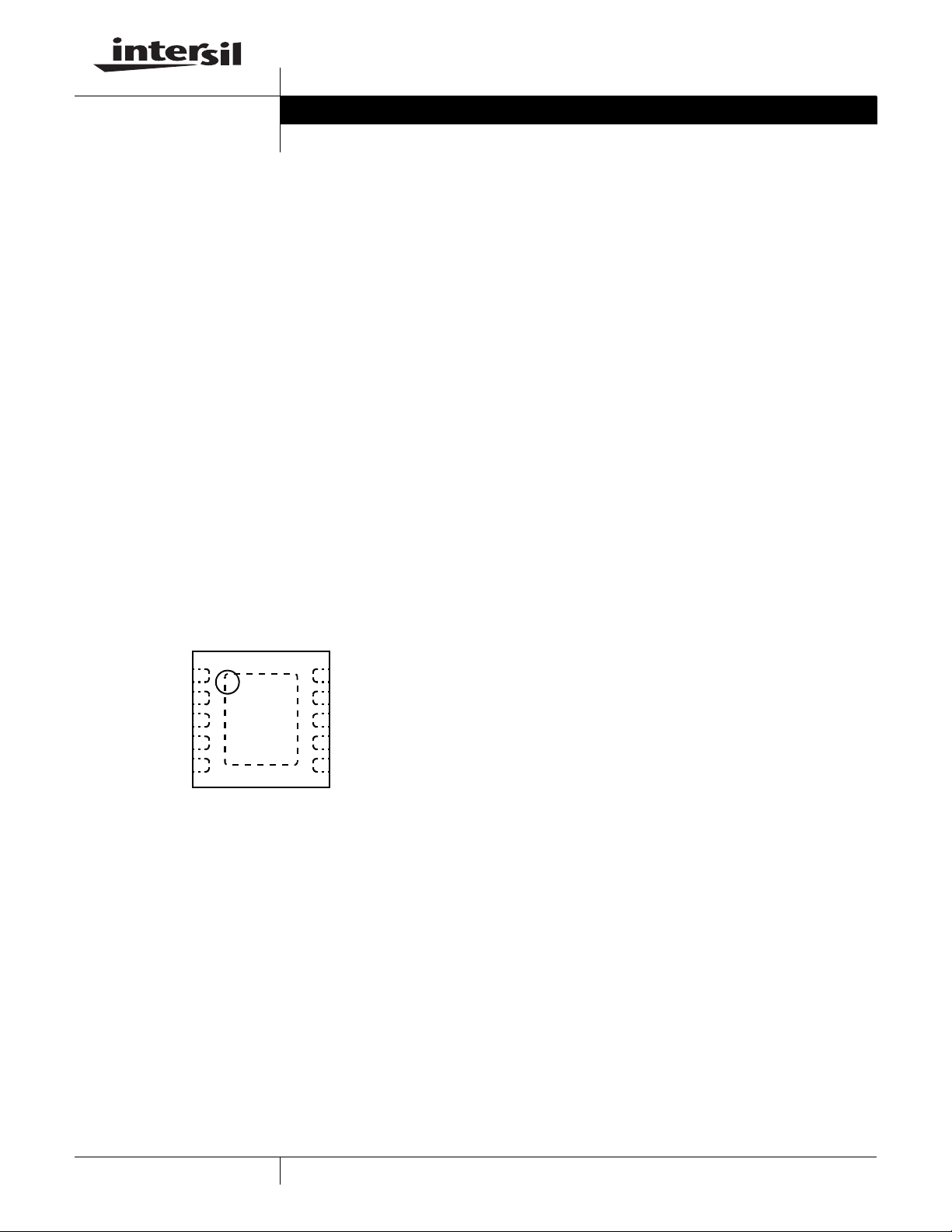
Pinout
ISL9011A
(10 LD 3x3 DFN)
TOP VIEW
VIN
EN1
EN2
CBYP
NC
1
2
3
4
5
10
VO1
9
VO2
8
NC
NC
7
6
GND
FN6437.1
Features
• Integrates two high performance LDOs
- VO1 - 150mA output
- VO2 - 300mA output
• Excellent transient response to large current steps
• Excellent load regulation: <1% voltage change across full
range of load current
• High PSRR: 70dB @ 1kHz
• Wide input voltage capability: 2.3V to 6.5V
• Extremely low quiescent current: 45µA (both LDOs active)
• Low dropout voltage: typically 120mV @ 150mA
• Low output noise: typically 30µV
@ 100µA (1.5V)
RMS
• Stable with 1µF to 10µF ceramic capacitors
• Separate enable pins for each LDO
• Soft-start to limit input current surge during enable
• Current limit and overheat protection
• ±1.8% accuracy over all operating conditions
• Tiny 10 Ld 3mmx3mm DFN package
• -40°C to +85°C operating temperature range
• Pin compatible with Micrel MIC2211
• Pb-free (RoHS compliant)
Applications
• PDAs, Cell Phones and Smart Phones
• Portable Instruments, MP3 Players
• Handheld Devices including Medical Handhelds
1
CAUTION: These devices are sensitive to electrostatic discharge; follow proper IC Handling Procedures.
1-888-INTERSIL or 1-888-468-3774
| Intersil (and design) is a registered trademark of Intersil Americas Inc.
All other trademarks mentioned are the property of their respective owners.
Copyright © Intersil Americas Inc. 2007, 2008. All Rights Reserved.

Ordering Information
www.BDTIC.com/Intersil
ISL9011A
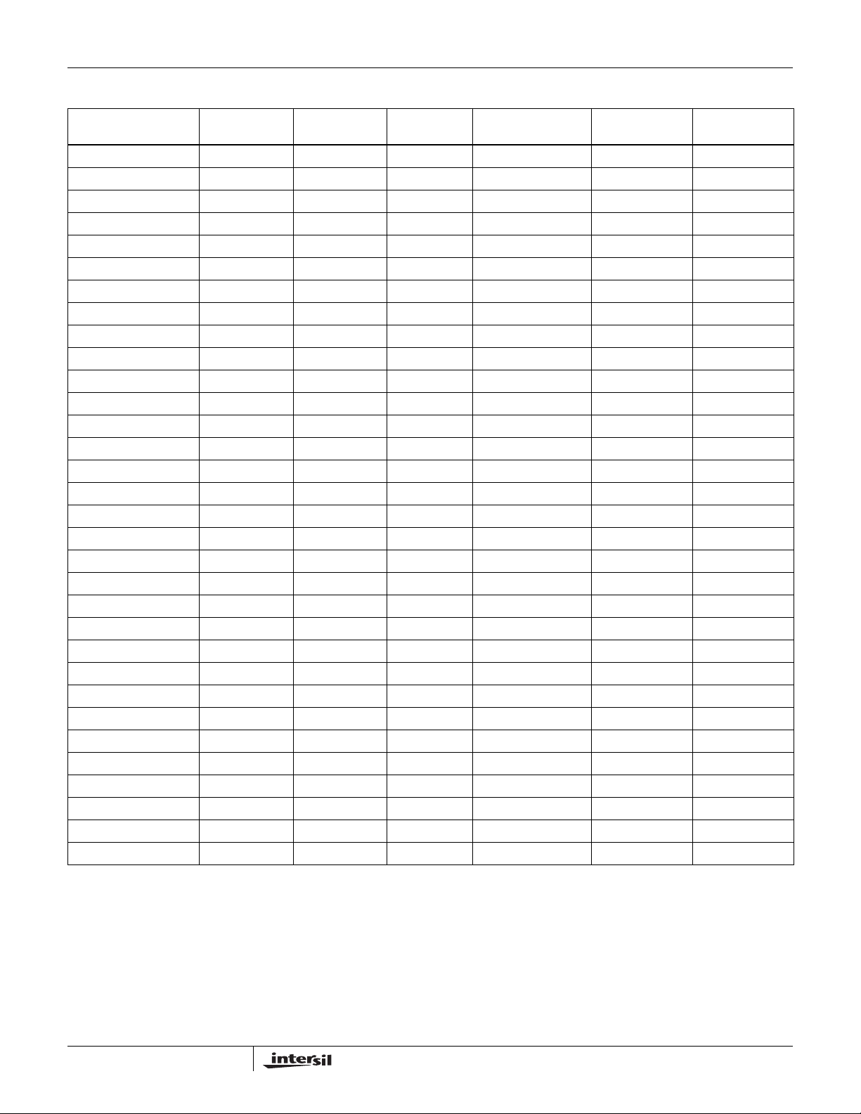
PART NUMBER
(Notes 1, 2, 3) PART MARKING
ISL9011AIRNNZ DGPA 3.3 3.3 -40 to +85 10 Ld 3x3 DFN L10.3x3C
ISL9011AIRNJZ DGNA 3.3 2.8 -40 to +85 10 Ld 3x3 DFN L10.3x3C
ISL9011AIRNFZ DGMA 3.3 2.5 -40 to +85 10 Ld 3x3 DFN L10.3x3C
ISL9011AIRNCZ DGLA 3.3 1.8 -40 to +85 10 Ld 3x3 DFN L10.3x3C
ISL9011AIRMNZ DGKA 3.0 3.3 -40 to +85 10 Ld 3x3 DFN L10.3x3C
ISL9011AIRMMZ DGJA 3.0 3.0 -40 to +85 10 Ld 3x3 DFN L10.3x3C
ISL9011AIRMGZ DGHA 3.0 2.7 -40 to +85 10 Ld 3x3 DFN L10.3x3C
ISL9011AIRLLZ DGGA 2.9 2.9 -40 to +85 10 Ld 3x3 DFN L10.3x3C
ISL9011AIRKNZ DGEA 2.85 3.3 -40 to +85 10 Ld 3x3 DFN L10.3x3C
ISL9011AIRKKZ DGDA 2.85 2.85 -40 to +85 10 Ld 3x3 DFN L10.3x3C
ISL9011AIRKJZ DGCA 2.85 2.8 -40 to +85 10 Ld 3x3 DFN L10.3x3C
ISL9011AIRKFZ DGBA 2.85 2.5 -40 to +85 10 Ld 3x3 DFN L10.3x3C
ISL9011AIRKPZ DGFA 2.85 1.85 -40 to +85 10 Ld 3x3 DFN L10.3x3C
ISL9011AIRKCZ DFYA 2.85 1.8 -40 to +85 10 Ld 3x3 DFN L10.3x3C
ISL9011AIRJNZ DFVA 2.8 3.3 -40 to +85 10 Ld 3x3 DFN L10.3x3C
ISL9011AIRJMZ DFTA 2.8 3.0 -40 to +85 10 Ld 3x3 DFN L10.3x3C
ISL9011AIRJRZ DWFA 2.8 2.6 -40 to +85 10 Ld 3x3 DFN L10.3x3C
ISL9011AIRJCZ DFSA 2.8 1.8 -40 to +85 10 Ld 3x3 DFN L10.3x3C
ISL9011AIRJBZ DFRA 2.8 1.5 -40 to +85 10 Ld 3x3 DFN L10.3x3C
ISL9011AIRGPZ DFPA 2.7 1.85 -40 to +85 10 Ld 3x3 DFN L10.3x3C
ISL9011AIRGCZ DFNA 2.7 1.8 -40 to +85 10 Ld 3x3 DFN L10.3x3C
ISL9011AIRFJZ DFMA 2.5 2.8 -40 to +85 10 Ld 3x3 DFN L10.3x3C
ISL9011AIRFDZ DFLA 2.5 2.0 -40 to +85 10 Ld 3x3 DFN L10.3x3C
ISL9011AIRFCZ DFKA 2.5 1.8 -40 to +85 10 Ld 3x3 DFN L10.3x3C
ISL9011AIRPLZ DGRA 1.85 2.9 -40 to +85 10 Ld 3x3 DFN L10.3x3C
ISL9011AIRPPZ DGSA 1.85 1.85 -40 to +85 10 Ld 3x3 DFN L10.3x3C
ISL9011AIRCJZ DFJA 1.8 2.8 -40 to +85 10 Ld 3x3 DFN L10.3x3C
ISL9011AIRCCZ DFHA 1.8 1.8 -40 to +85 10 Ld 3x3 DFN L10.3x3C
ISL9011AIRBLZ DFGA 1.5 2.9 -40 to +85 10 Ld 3x3 DFN L10.3x3C
ISL9011AIRBJZ DFFA 1.5 2.8 -40 to +85 10 Ld 3x3 DFN L10.3x3C
ISL9011AIRBCZ DFEA 1.5 1.8 -40 to +85 10 Ld 3x3 DFN L10.3x3C
ISL9011AIRBBZ DFDA 1.5 1.5 -40 to +85 10 Ld 3x3 DFN L10.3x3C
NOTES:
1. Add “-T” suffix for tape and reel. Please refer to TB347 for details on reel specifications.
2. For availability and lead time of devices with voltage combinations not listed in the table, contact Intersil Marketing.
3. These Intersil Pb-free plastic packaged products employ special Pb-free material sets; molding compounds/die attach materials and 100% matte
tin plate PLUS ANNEAL - e3 termination finish, which is RoHS compliant and compatible with both SnPb and Pb-free soldering operations.
Intersil Pb-free products are MSL classified at Pb-free peak reflow temperatures that meet or exceed the Pb-free requirements of IPC/JEDEC
J STD-020.
VO1 VOLTAGE
(V)
VO2 VOLTAGE
(V) TEMP RANGE (°C)
PACKAGE
(Pb-free) PKG. DWG. #
2
FN6437.1
March 7, 2008

ISL9011A
www.BDTIC.com/Intersil
Absolute Maximum Ratings Thermal Information
Supply Voltage (VIN) . . . . . . . . . . . . . . . . . . . . . . . . . . . . . . . . +7.1V
V
1, VO2 Pins. . . . . . . . . . . . . . . . . . . . . . . . . . . . . . . . . . . . . +3.6V
O
All Other Pins . . . . . . . . . . . . . . . . . . . . . . . . . . -0.3 to (V
IN
+ 0.3)V
Recommended Operating Conditions
Ambient Temperature Range (TA) . . . . . . . . . . . . . . .-40°C to +85°C
Supply Voltage (VIN) . . . . . . . . . . . . . . . . . . . . . . . . . . .2.3V to 6.5V
CAUTION: Do not operate at or near the maximum ratings listed for extended periods of time. Exposure to such conditions may adversely impact product reliability and
result in failures not covered by warranty.
NOTES:
is measured in free air with the component mounted on a high effective thermal conductivity test board with “direct attach” features. See
4. θ
JA
Tech Brief TB379.
5. For θ
, the “case temp” location is the center of the exposed metal pad on the package underside.
JC
Thermal Resistance (Notes 4, 5) θ
10 Ld 3x3 DFN Package . . . . . . . . . . . 50 10
Junction Temperature Range . . . . . . . . . . . . . . . . .-40°C to +125°C
Operating Temperature Range . . . . . . . . . . . . . . . . .-40°C to +85°C
Storage Temperature Range . . . . . . . . . . . . . . . . . .-65°C to +150°C
Pb-free reflow profile . . . . . . . . . . . . . . . . . . . . . . . . . .see link below
http://www.intersil.com/pbfree/Pb-FreeReflow.asp
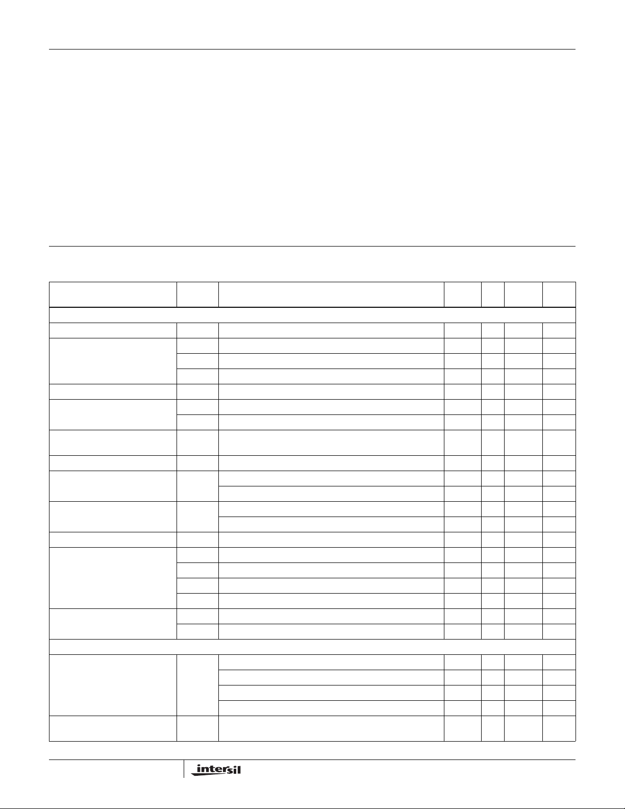
Electrical Specifications Unless otherwise noted, all parameters are guaranteed over the operational supply voltage and temperature
range of the device as follows: T
C
= 1µF; CO = 1µF; C
IN
PARAMETER SYMBOL TEST CONDITIONS
DC CHARACTERISTICS
Supply Voltage V
Ground Current Quiescent condition: I
Shutdown Current I
UVLO Threshold V
Regulation Voltage Accuracy Variation from nominal voltage output, V
Line Regulation V
Load Regulation I
Maximum Output Current I
Internal Current Limit I
Dropout Voltage (Note 6) V
Thermal Shutdown Temperature T
AC CHARACTERISTICS
Ripple Rejection I
Output Noise Voltage I
IN
I
DD1
I
DD2
DDS
UV+
V
UV-
MAX
LIM
DO1IO
V
DO2IO
V
DO3IO
V
DO4IO
SD+
T
SD-
One LDO active 25 40 µA
Both LDO active 45 60 µA
@ +25°C 0.1 1.0 µA
T
= -40°C to +125°C
J
IN
OUT
I
OUT
VO1: Continuous 150 mA
VO2: Continuous 300 mA
= 150mA; VO > 2.1V (VO1) 125 200 mV
= 300mA; VO < 2.5V (VO2) 300 500 mV
= 300mA; 2.5V ≤ VO ≤ 2.8V (VO2) 250 400 mV
= 300mA; VO > 2.8V (VO2) 200 325 mV
= 10mA, VIN = 2.8V(min), VO = 1.8V, C
O
@ 1kHz 70 dB
@ 10kHz 55 dB
@ 100kHz 40 dB
= 100μA, VO = 1.5V, TA = +25°C, C
O
BW = 10Hz to 100kHz
BYP
= (V
OUT
= 100µA to 150mA (VO1 and VO2) 0.1 0.7 %
= 100µA to 300mA (VO2) 1.0 %
= -40°C to +85°C; VIN = (VO + 1.0V) to 6.5V with a minimum VIN of 2.3V;
A
= 0.01µF
MIN
(Note 7) TYP
2.3 6.5 V
= 0µA; IO2 = 0µA
O1
1.9 2.1 2.3 V
1.6 1.8 2.0 V
= VO+ 0.5 to 5.5V ,
IN
+ 1.0V relative to highest output voltage) to 5.5V -0.2 0 0.2 %/V
= 0.1µF
BYP
= 0.1µF
BYP
-1.8 +1.8 %
350 475 600 mA
(°C/W) θJC (°C/W)
JA
MAX
(Note 7) UNITS
145 °C
110 °C
30 µV
RMS
3
FN6437.1
March 7, 2008

ISL9011A
www.BDTIC.com/Intersil
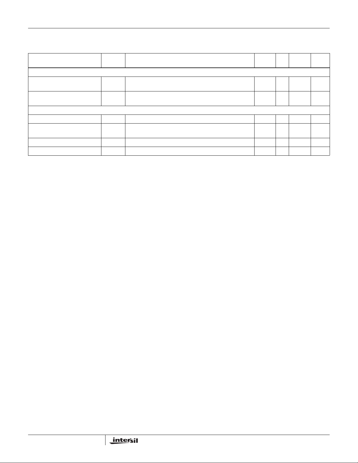
Electrical Specifications Unless otherwise noted, all parameters are guaranteed over the operational supply voltage and temperature
range of the device as follows: T
= 1µF; CO = 1µF; C
C
IN
PARAMETER SYMBOL TEST CONDITIONS
DEVICE START-UP CHARACTERISTICS
Device Enable Time t
LDO Soft-Start Ramp Rate t
EN1, EN2 PIN CHARACTERISTICS
Input Low Voltage V
Input High Voltage V
Input Leakage Current I
Pin Capacitance C
NOTE:
6. VOx = 0.98*VOx(NOM); Valid for VOx greater than 1.85V.
7. Parts are 100% tested at +25°C. Temperature limits established by characterization and are not production tested.
IL
Time from assertion of the ENx pin to when the output voltage
EN
reaches 95% of the VO(nom)
Slope of linear portion of LDO output voltage ramp during
SSR
start-up
IL
IH
, I
IH
Informative 5 pF
PIN
BYP
= -40°C to +85°C; VIN = (VO + 1.0V) to 6.5V with a minimum VIN of 2.3V;
A
= 0.01µF (Continued)
MIN
(Note 7) TYP
-0.3 0.5 V
1.4 VIN+
MAX
(Note 7) UNITS
250 500 µs
30 60 µs/V
0.3
0.1 µA
V
4
FN6437.1
March 7, 2008
 Loading...