®
www.BDTIC.com/Intersil
ISL9008A
Data Sheet March 11, 2008
Low Noise LDO with Low IQ, High PSRR
ISL9008A is a high performance single low noise, high
PSRR LDO that delivers a continuous 150mA of load
current. It has a low standby current and is stable with 1μF of
MLCC output capacitance with an ESR of up to 200mΩ.
The ISL9008A has a high PSRR of 65dB and output noise
less than 45μV
. When coupled with a no load quiescent
RMS
current of 46μA (typical), and 0.5μA shutdown current, the
ISL9008A is an ideal choice for portable wireless equipment.
The ISL9008A comes in several fixed voltage options with
±1.8% output voltage accuracy over-temperature, line and
load. Other output voltage options may be available upon
request.
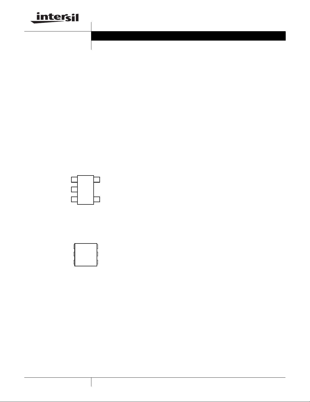
Pinouts
ISL9008A
(5 LD SC-70)
TOP VIEW
VIN
GND
EN
1
2
354
VO
NC
FN6300.4
Features
• High performance LDO with 150mA continuous output
• Excellent transient response to large current steps
• Excellent load regulation:
<0.1% voltage change across full range of load current
• High PSRR: 65dB @ 1kHz
• Wide input voltage capability: 2.3V to 6.5V
• Very low quiescent current: 46µA
• Low dropout voltage: typically 200mV @ 150mA
• Low output noise: typically 45µV
• Stable with 1µF to 4.7µF ceramic capacitors
• Shutdown pin turns off LDO with 1µA (max) standby
current
• Soft-start limits input current surge during enable
• Current limit and overheat protection
• ±1.8% accuracy over all operating conditions
• 5 Ld SC-70 package or 6 Ld µTDFN package
• -40°C to +85°C operating temperature range
• Pb-free (RoHS compliant)
@ 100µA (1.5V)
RMS
ISL9008A
(6 LD 1.6x1.6 µTDFN)
TOP VIEW
VO
GND
NC
1
2
3
6
5
4
VIN
NC5
EN
Applications
• PDAs, cell phones and smart phones
• Portable instruments, MP3 players
• Handheld devices including medical handhelds
1
CAUTION: These devices are sensitive to electrostatic discharge; follow proper IC Handling Procedures.
1-888-INTERSIL or1-888-468-3774
| Intersil (and design) is a registered trademark of Intersil Americas Inc.
Copyright © Intersil Americas Inc. 2006, 2007, 2008. All Rights Reserved.
All other trademarks mentioned are the property of their respective owners.

ISL9008A
www.BDTIC.com/Intersil
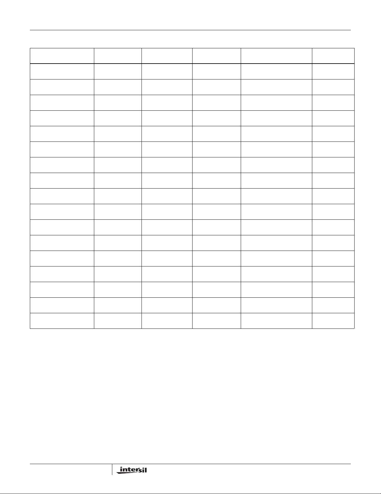
Ordering Information
PART NUMBER
(Note 4)
ISL9008AIENZ-T
(Note 2)
ISL9008AIEMZ-T
(Note 2)
ISL9008AIEKZ-T
(Note 2)
ISL9008AIEJZ-T
(Note 2)
ISL9008AIEHZ-T
(Note 2)
ISL9008AIEFZ-T
(Note 2)
ISL9008AIETZ-T
(Note 2)
ISL9008AIECZ-T
(Note 2)
ISL9008AIEBZ-T
(Note 2)
ISL9008AIRUBZ-T
(Note 3)
ISL9008AIRUCZ-T
(Note 3)
ISL9008AIRUFZ-T
(Note 3)
ISL9008AIRUHZ-T
(Note 3)
ISL9008AIRUJZ-T
(Note 3)
ISL9008AIRUKZ-T
(Note 3)
ISL9008AIRUMZ-T
(Note 3)
ISL9008AIRUNZ-T
(Note 3)
NOTES:
1. For other output voltages, contact Intersil Marketing.
2. These Intersil Pb-free plastic packaged products employ special Pb-free material sets; molding compounds/die attach materials and 100% matte
tin plate PLUS ANNEAL - e3 termination finish, which is RoHS compliant and compatible with both SnPb and Pb-free soldering operations. Intersil
Pb-free products are MSL classified at Pb-free peak reflow temperatures that meet or exceed the Pb-free requirements of IPC/JEDEC J STD-020.
3. These Intersil Pb-free plastic packaged products employ special Pb-free material sets; molding compounds/die attach materials and NiPdAu plate
- e4 termination finish, which is RoHS compliant and compatible with both SnPb and Pb-free soldering operations. Intersil Pb-free products are
MSL classified at Pb-free peak reflow temperatures that meet or exceed the Pb-free requirements of IPC/JEDEC J STD-020.
4. Please refer to TB347 for details on reel specifications.
PART
MARKING
CBV 3.3 -40 to +85 5 Ld SC-70 P5.049
CBT 3.0 -40 to +85 5 Ld SC-70 P5.049
CBS 2.85 -40 to +85 5 Ld SC-70 P5.049
CBR 2.8 -40 to +85 5 Ld SC-70 P5.049
CBP 2.75 -40 to +85 5 Ld SC-70 P5.049
CBN 2.5 -40 to +85 5 Ld SC-70 P5.049
CDW 1.9 -40 to +85 5 Ld SC-70 P5.049
CBM 1.8 -40 to +85 5 Ld SC-70 P5.049
CBL 1.5 -40 to +85 5 Ld SC-70 P5.049
P 1.5 -40 to +85 6 Ld µTDFN L6.1.6x1.6A
Q 1.8 -40 to +85 6 Ld µTDFN L6.1.6x1.6A
R 2.5 -40 to +85 6 Ld µTDFN L6.1.6x1.6A
S 2.75 -40 to +85 6 Ld µTDFN L6.1.6x1.6A
T 2.8 -40 to +85 6 Ld µTDFN L6.1.6x1.6A
V 2.85 -40 to +85 6 Ld µTDFN L6.1.6x1.6A
W 3.0 -40 to +85 6 Ld µTDFN L6.1.6x1.6A
Y 3.3 -40 to +85 6 Ld µTDFN L6.1.6x1.6A
VO VOLTAGE (V)
(Note 1)
TEMP.
RANGE (°C) PACKAGE PKG. DWG. #
2
FN6300.4
March 11, 2008

ISL9008A
www.BDTIC.com/Intersil
Absolute Maximum Ratings Thermal Information
Supply Voltage (VIN) . . . . . . . . . . . . . . . . . . . . . . . . . . . . . . . . +7.1V
V
Pin . . . . . . . . . . . . . . . . . . . . . . . . . . . . . . . . . . . . . . . . . . . +3.6V
O
All Other Pins . . . . . . . . . . . . . . . . . . . . . . . . . . -0.3V to (VIN+0.3V)
Recommended Operating Conditions
Ambient Temperature Range (TA) . . . . . . . . . . . . . . .-40°C to +85°C
Supply Voltage (V
CAUTION: Do not operate at or near the maximum ratings listed for extended periods of time. Exposure to such conditions may adversely impact product reliability and
result in failures not covered by warranty.
NOTES:
is measured with the component mounted on a high effective thermal conductivity test board in free air. See Tech Brief TB379 for details.
5. θ
JA
6. θ
is measured in free air with the component mounted on a high effective thermal conductivity test board with “direct attach” features. See
JA
Tech Brief TB379.
) . . . . . . . . . . . . . . . . . . . . . . . . . . . . 2.3 to 6.5V
IN
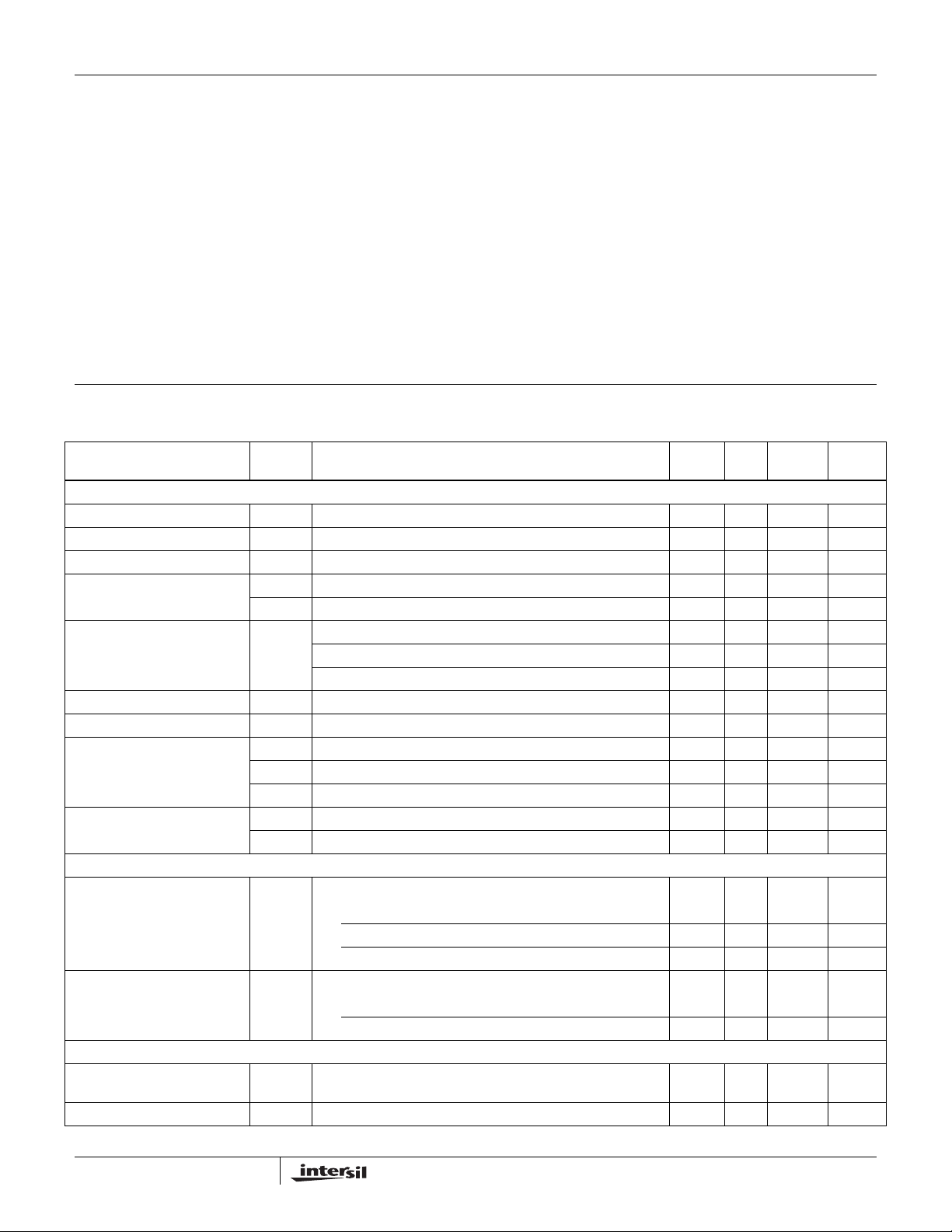
Electrical Specifications Unless otherwise noted, all parameters are established over the operational supply voltage and temperature
range of the device as follows:
= -40°C to +85°C; V
T
A
PARAMETER SYMBOL TEST CONDITIONS
DC CHARACTERISTICS
Supply Voltage V
Ground Current I
Shutdown Current I
UVLO Threshold V
Regulation Voltage Accuracy Initial accuracy at V
Maximum Output Current I
Internal Current Limit I
Drop-out Voltage (Note 8) V
Thermal Shutdown
Temperature
AC CHARACTERISTICS
Ripple Rejection (Note 7) I
Output Noise Voltage (Note 7) V
DEVICE START-UP CHARACTERISTICS
Device Enable Time t
LDO Soft-start Ramp Rate t
IN
DD
DDS
UV+
V
UV-
MAX
LIM
DO1IO
V
DO2IO
V
DO3IO
T
SD+
T
SD-
EN
SSR
Quiescent condition: IO = 0µA 46 66 µA
= VO + 0.5V to 6.5V, IO = 10μA to150mA, TJ = +25°C -0.8 +0.8 %
V
IN
= VO + 0.5V to 6.5V , IO = 10μA to 150mA, TJ = -40°C to +125°C -1.8 +1.8 %
V
IN
Continuous 150 mA
= 150mA; VO < 2.5V 300 500 mV
= 150mA; 2.5V ≤ VO ≤ 2.8V 250 400 mV
= 150mA; 2.8V < V
= 10mA, V
O
@ 1kHz 65 dB
@ 10kHz 45 dB
@ 100kHz 35 dB
= 1.5V, TA = +25°C
O
BW = 10Hz to 100kHz, I
BW = 10Hz to 100kHz, IO = 10mA 65 µV
Time from assertion of the ENx pin to when the output voltage
reaches 95% of the VO(nom)
Slope of linear portion of LDO output voltage ramp during st art-up 30 60 µs/V
= (VO + 0.5V) to 6.5V with a minimum VIN of 2.3V; C
IN
= VO + 0.5V, IO = 10mA, TJ = +25°C -0.7 +0.7 %
IN
O
= 2.8V(min), VO = 1.8V
IN
Thermal Resistance θ
5 Ld SC-70 Package (Note 5) . . . . . . . . . . . . . . . . . 231
6 Ld µTDFN Package (Note 6) . . . . . . . . . . . . . . . . 125
Junction Temperature Range . . . . . . . . . . . . . . . . .-40°C to +125°C
Operating Temperature Range . . . . . . . . . . . . . . . . .-40°C to +85°C
Storage Temperature Range . . . . . . . . . . . . . . . . . .-65°C to +150°C
Pb-free reflow profile . . . . . . . . . . . . . . . . . . . . . . . . . .see link below
http://www.intersil.com/pbfree/Pb-FreeReflow.asp
= 1µF; CO = 1µF.
IN
MIN
(Note 9) TYP
2.3 6.5 V
1.9 2.1 2.3 V
1.6 1.8 2.0 V
175 265 355 mA
200 325 mV
140 °C
110 °C
= 100µA 45 µV
O
250 500 µs
MAX
(Note 9) UNITS
0.5 1.2 µA
(°C/W)
JA
RMS
RMS
3
FN6300.4
March 11, 2008

ISL9008A
www.BDTIC.com/Intersil
Electrical Specifications Unless otherwise noted, all parameters are established over the operational supply voltage and temperature
range of the device as follows:
= -40°C to +85°C; V
T
A
PARAMETER SYMBOL TEST CONDITIONS
= (VO + 0.5V) to 6.5V with a minimum VIN of 2.3V; C
IN
= 1µF; CO = 1µF. (Continued)
IN
MIN
(Note 9) TYP
MAX
(Note 9) UNITS
EN PIN CHARACTERISTICS
Input Low Voltage V
Input High Voltage V
Input Leakage Current I
Pin Capacitance C
IL
IH
, I
IL
IH
Informative 5 pF
PIN
-0.3 0.4 V
1.4 VIN+0.3 V
0.1 μA
NOTES:
7. Limits established by characterization and are not production tested.
8. VOx = 0.98*VOx(NOM); Valid for VOx greater than 1.85V.
9. Parts are 100% tested at +25°C. Temperature limits established by characterization and are not production tested.
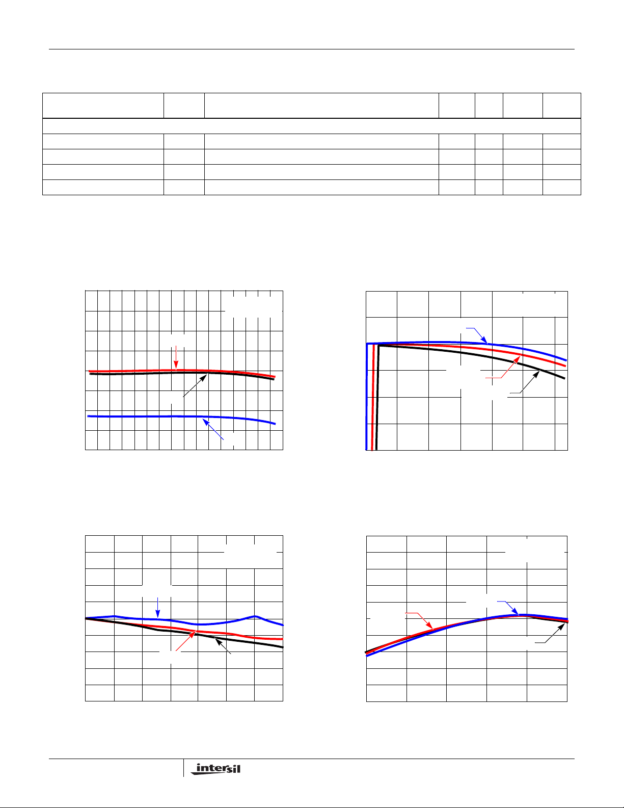
Typical Performance Curves
(%)
O
0.8
0.6
0.4
0.2
+25°C
VO = 3.3V
I
= 0mA
LOAD
0.2
0.1
0.0
VO = 3.3V
+25°C
IO = 0mA
0.0
-0.2
-0.4
OUTPUT VOLTAGE, V
-0.6
-0.8
3.8 4.2 6.25.8
+85°C
-40°C
INPUT VOLTAGE (V)
FIGURE 1. OUTPUT VOLT AGE vs INPUT VOL T AGE
(3.3V OUTPUT)
1.0
V
0.8
0.6
0.4
0.2
0.0
-0.2
-0.4
-0.6
OUTPUT VOLTAGE CHANGE (%)
-0.8
-1.0
0 25 50 75 100 125 150 175
-40°C
+25°C
LOAD CURRENT - IO (mA)
IN
V
= 3.3V
O
+85°C
= 3.8V
6.63.4 4.6 5.0 5.4
-0.1
-0.2
-0.3
OUTPUT VOLTAGE CHANGE (%)
-0.4
3.3 3.8 4.3 4.8 5.3 5.8 6.3
IO = 75mA
= 150mA
I
O
INPUT VOLTAGE (V)
FIGURE 2. OUTPUT VOLT AGE CHANGE (%) vs INPUT
VOLTAGE (3.3V OUTPUT)
0.10
I
= 150mA
O
VIN = 3.8V
V
OUTPUT VOLTAGE (%)
0.08
0.06
0.04
0.02
0.00
-0.02
-0.04
-0.06
-0.08
-0.10
IO = 0mA
IO = 75mA
-25 0 25 85-40
TEMPERATURE (°C)
FIGURE 3. OUTPUT VOLTAGE vs LOAD CURRENT FIGURE 4. OUTPUT VOLTAGE vs TEMPERATURE
= 3.3V
O
55
4
FN6300.4
March 11, 2008
 Loading...