®
www.BDTIC.com/Intersil
ISL9000AMRNCEP
Data Sheet
Dual LDO with Low Noise, Very High
PSRR and Low I
ISL9000AMRNCP is a high performance dual LDO capable
of sourcing 100mA current from each output. It has a low
standby current and very high PSRR and is stable with
output capacitance of 1µF to 10µF with ESR of up to 200mΩ.
The device integrates an individual Power-On-Reset (POR)
function for each output. The POR delay for VO2 can be
externally programmed by connecting a timing capacitor to
the CPOR pin. The POR delay for VO1 is internally fixed at
approximately 2ms. A reference bypass pin is also provided
for connecting a noise filtering capacitor for low noise and
high-PSRR applications.
The quiescent current is typically only 42µA with both LDO’s
enabled and active. Separate enable pins control each
individual LDO output. When both enable pins are low, the
device is in shutdown, typically drawing less than 0.1µA.
Output voltage for the LDO are VOUT1 = 3.3V and
VOUT2 = 1.8V.
Q
Device Information
The specifications for an Enhanced Product (EP) device are
defined in a Vendor Item Drawing (VID), which is controlled
by the Defense Supply Center in Columbus (DSCC).
“Hot-links” to the applicable VID and other supporting
application information are provided on our website.
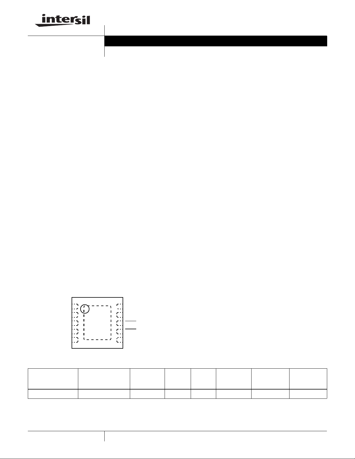
Pinout
ISL9000AMNCEP
(10 LD 3X3 DFN)
TOP VIEW
December 12, 2007
FN6620.0
Features
• Integrates Two 100mA High Performance LDO’s
•I
per Channel is 50mA at TJ = +150°C
OUT
• Excellent Transient Response to Large Current Steps
• ±1.8% Accuracy Over all Operating Conditions
• Excellent Load Regulation:
< 0.1% Voltage Change Across Full Range of Load
Current
• Low Output Noise: Typically 30µV
@ 100µA (1.5V)
rms
• Very High PSRR: 90dB @ 1kHz
• Extremely Low Quiescent Current: 42µA (both LDOs
active)
• Wide Input Voltage Capability: 2.3V to 5.5V
• Low Dropout Voltage: Typically 200mV @ 100mA
• Stable with 1µF to 10µF Ceramic Capacitors
• Separate Enable and POR Pins for Each LDO
• Soft-Start and Staged Turn-On to Limit Input Current
Surge During Enable
• Current Limit and Overheat Protection
• Tiny 10 Ld 3x3mm DFN Package
• -55°C to +125°C Operating Temperature Range
Applications
• PDAs, Cell Phones and Smart Phones
• Portable Instruments, MP3 Players
• Handheld Devices including Medical Handheld
VIN
EN1
EN2
CBYP
CPOR
1
2
3
4
5
VO1
10
9
VO2
8
POR2
7
POR1
6
GND
Ordering Information
VENDOR PART
NUMBER
(Notes 1, 2)
ISL9000AMRNCEP V62/08609-01XB DKTA 3.3 1.8 -55 to +125 10 Ld 3x3 DFN L10.3x3C
NOTES:
1. Add -T to part number for tape and reel.
2. Devices must be procured to the VENDOR PART NUMBER.
VENDOR ITEM
DRAWING
1
PART
MARKING
1-888-INTERSIL or 1-888-468-3774
VO1
VOLTAGE
(V)
CAUTION: These devices are sensitive to electrostatic discharge; follow proper IC Handling Procedures.
VO2
VOLTAGE
(V)
TEMP RANGE
| Intersil (and design) is a registered trademark of Intersil Americas Inc.
All other trademarks mentioned are the property of their respective owners.
PKG
(°C) PACKAGE
Copyright © Intersil Americas Inc. 2007. All Rights Reserved.
DWG. #

ISL9000AMRNCEP
www.BDTIC.com/Intersil
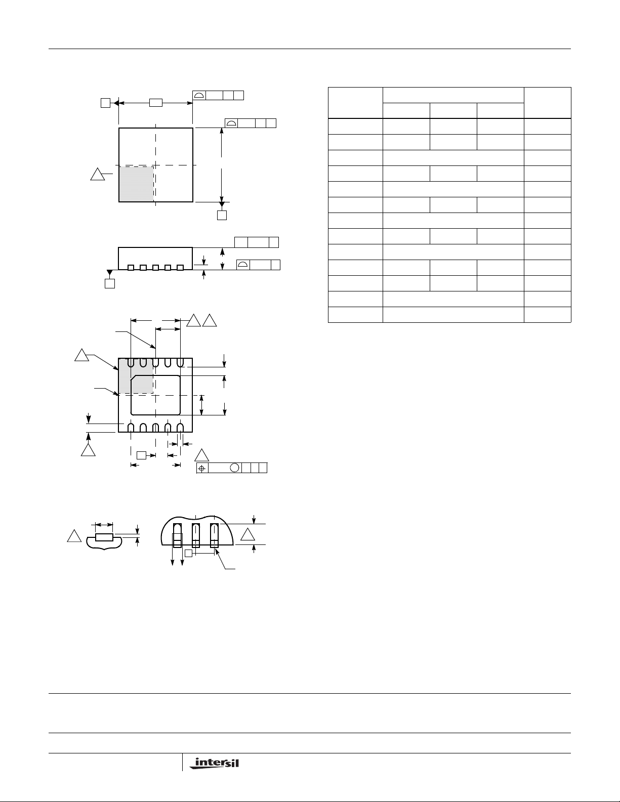
Dual Flat No-Lead Plastic Package (DFN)
(DATUM B)
6
INDEX
AREA
(DATUM A)
NX (b)
5
SECTION "C-C"
6
INDEX
AREA
SEATING
PLANE
NX L
8
A
C
D
TOP VIEW
SIDE VIEW
D2
D2/2
12
N
N-1
e
(Nd-1)Xe
REF.
BOTTOM VIEW
(A1)
2X
A3
E2/2
NX b
5
C
L
e
CC
FOR ODD TERMINAL/SIDE
E
87
0.10
ABC0.10
2X
0.10
//
A
NX k
E2
M
TERMINAL TIP
9
0.10
0.08
L
CB
C
C
BAC
L10.3x3C
10 LEAD DUAL FLAT NO-LEAD PLASTIC PACKAGE
MILLIMETERS
SYMBOL
A
A1 - A3
b
D
0.85 0.90 0.95
0.05
0.20 REF
0.20 0.25 0.30 5, 8
3.00 BSC
D2 2.33 2.38 2.43 7, 8
E 3.00 BSC
E2
1.59
1.64 1.69 7, 8
e 0.50 BSC
k0.20
L
0.35 0.40 0.45
N
Nd
---
10
53
NOTES:
1. Dimensioning and tolerancing conform to ASME Y14.5-1994.
2. N is the number of terminals.
3. Nd refers to the number of terminals on D.
4. All dimensions are in millimeters. Angles are in degrees.
5. Dimension b applies to the metallized terminal and is measured
between 0.15mm and 0.30mm from the terminal tip.
6. The configuration of the pin #1 identifier is optional, but must be
located within the zone indicated. The pin #1 identi fier may be
either a mold or mark feature.
7. Dimensions D2 and E2 are for the exposed pads which provide
improved electrical and thermal performance.
8. Nominal dimensions are provided to assist with PCB Land
Pattern Design efforts, see Intersil Technical Brief TB389.
9. COMPLIANT TO JEDEC MO-229-WEED-3 except for
dimensions E2 & D2.
NOTESMIN NOMINAL MAX
-
-
-
-
-
-
8
2
Rev. 1 4/06
All Intersil U.S. products are manufactured, assembled and tested utilizing ISO9000 quality systems.
Intersil Corporation’s quality certifications can be viewed at www.intersil.com/design/quality
Intersil products are sold by description only. Intersil Corporation reserves the right to make changes in circuit design, software and/or specifications at any time without
notice. Accordingly, the reader is cautioned to verify that data sheets are current before placing orders. Information furnished by Intersil is believed to be accurate and
reliable. However, no responsibility is assumed by Intersil or its subsidiaries for its use; nor for any infringements of patents or other rights of third parties which may result
from its use. No license is granted by implic atio n or other wise u nde r any p a tent or patent rights of Intersil or its subsidi aries.
For information regarding Intersil Corporation and its products, see www.intersil.com
2
FN6620.0
 Loading...