intersil ISL9000A DATA SHEET

®
www.BDTIC.com/Intersil
ISL9000A
Data Sheet March 11, 2008
Dual LDO with Low Noise, Very High
PSRR and Low I
ISL9000A is a high performance dual LDO capable of
sourcing 300mA current from each output. It has a low
standby current and very high PSRR and is stable with
output capacitance of 1µF to 10µF with ESR of up to 200mΩ.
The device integrates an individual Power-On-Reset (POR)
function for each output. The POR delay for VO2 can be
externally programmed by connecting a timing capacitor to
the CPOR pin. The POR delay for VO1 is internally fixed at
approximately 2ms. A reference bypass pin is also provided
for connecting a noise filtering capacitor for low noise and
high-PSRR applications.
The quiescent current is typically only 42µA with both LDO’s
enabled and active. Separate enable pins control each
individual LDO output. When both enable pins are low, the
device is in shutdown, typically drawing less than 0.1µA.
Several combinations of voltage outputs are standard.
Output voltage options for each LDO range from 1.5V to
3.3V. Other output voltage options may be available upon
request.
Q
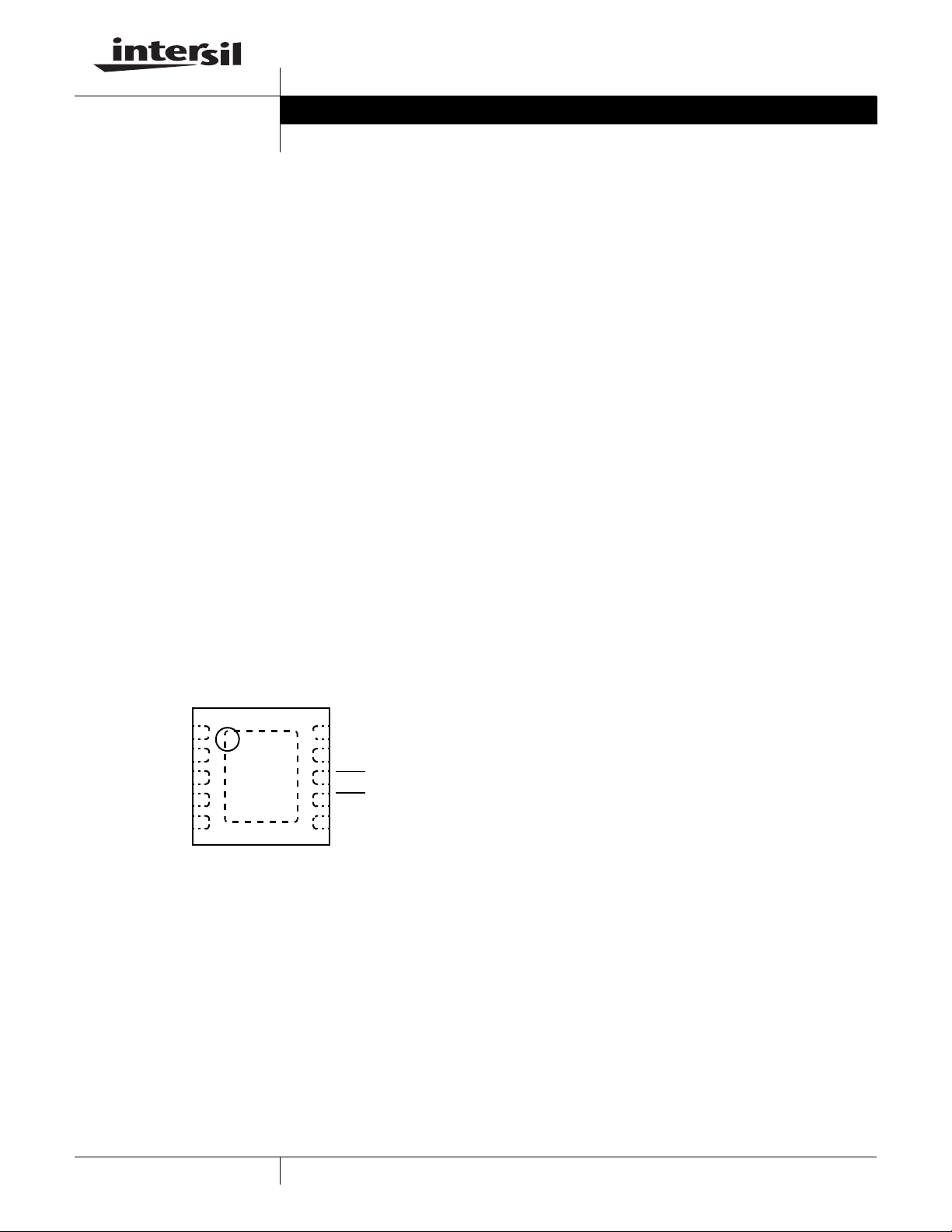
Pinout
ISL9000A
(10 LD 3X3 DFN)
TOP VIEW
VIN
EN1
EN2
CBYP
CPOR
1
2
3
4
5
VO1
10
9
VO2
8
POR2
7
POR1
6
GND
FN6391.1
Features
• Integrates two 300mA high performance LDOs
• Excellent transient response to large current steps
• ±1.8% accuracy over all operating conditions
• Excellent load regulation: < 0.1% voltage change across
full range of load current
• Low output noise: typically 30µV
@ 100µA (1.5V)
RMS
• Very high PSRR: 90dB @ 1kHz
• Extremely low quiescent current: 42µA (both LDOs active)
• Wide input voltage capability: 2.3V to 6.5V
• Low dropout voltage: typically 200mV @ 300mA
• Stable with 1µF to 10µF ceramic capacitors
• Separate enable and POR pins for each LDO
• Soft-start and staged turn-on to limit input current surge
during enable
• Current limit and overheat protection
• Tiny 10 Ld 3mmx3mm DFN package
• -40°C to +85°C operating temperature range
• Pb-free (RoHS compliant)
Applications
• PDAs, Cell Phones and Smart Phones
• Portable Instruments, MP3 Players
• Handheld Devices including Medical Handheld
1
CAUTION: These devices are sensitive to electrostatic discharge; follow proper IC Handling Procedures.
1-888-INTERSIL or 1-888-468-3774
| Intersil (and design) is a registered trademark of Intersil Americas Inc.
All other trademarks mentioned are the property of their respective owners.
Copyright © Intersil Americas Inc. 2007, 2008. All Rights Reserved.

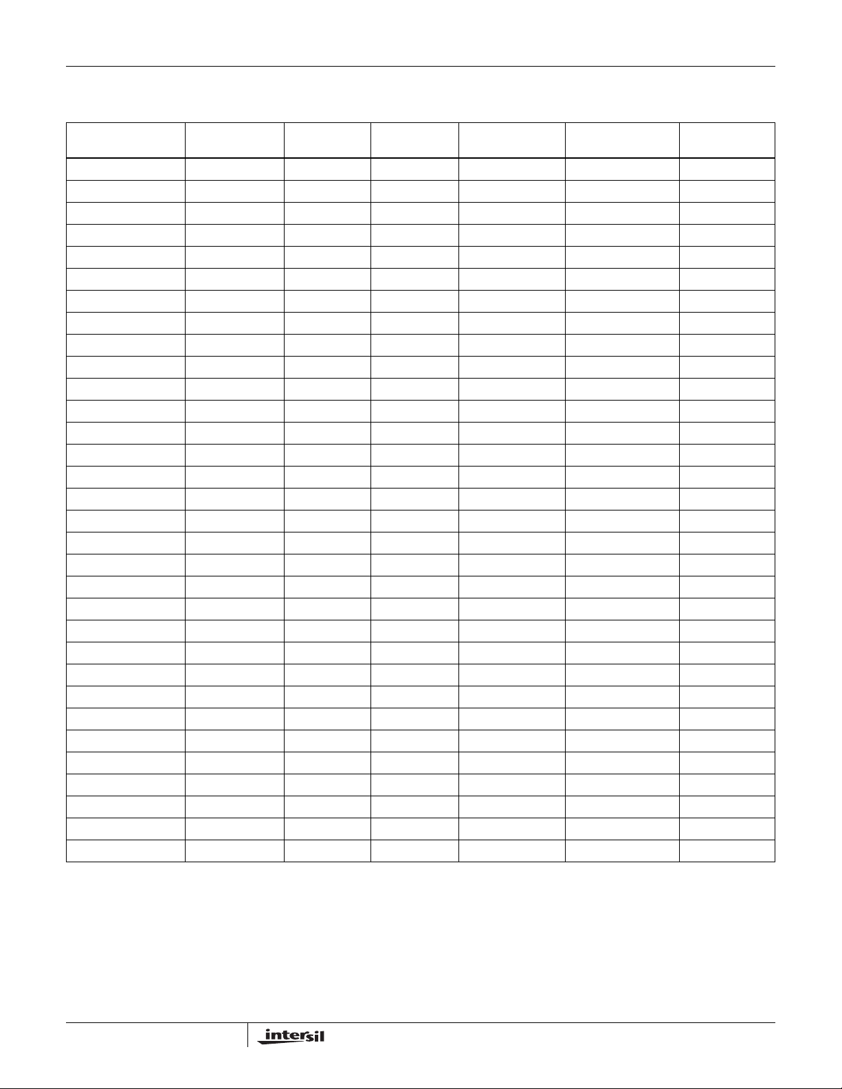
Ordering Information
www.BDTIC.com/Intersil
ISL9000A
PART NUMBER
(Notes 1, 3) PART MARKING
ISL9000AIRNNZ DEYA 3.3 3.3 -40 to +85 10 Ld 3x3 DFN L10.3x3C
ISL9000AIRNJZ DEWA 3.3 2.8 -40 to +85 10 Ld 3x3 DFN L10.3x3C
ISL9000AIRNFZ DEVA 3.3 2.5 -40 to +85 10 Ld 3x3 DFN L10.3x3C
ISL9000AIRNCZ DETA 3.3 1.8 -40 to +85 10 Ld 3x3 DFN L10.3x3C
ISL9000AIRMNZ DESA 3.0 3.3 -40 to +85 10 Ld 3x3 DFN L10.3x3C
ISL9000AIRMMZ DERA 3.0 3.0 -40 to +85 10 Ld 3x3 DFN L10.3x3C
ISL9000AIRMGZ DEPA 3.0 2.7 -40 to +85 10 Ld 3x3 DFN L10.3x3C
ISL9000AIRLLZ DENA 2.9 2.9 -40 to +85 10 Ld 3x3 DFN L10.3x3C
ISL9000AIRKNZ DELA 2.85 3.3 -40 to +85 10 Ld 3x3 DFN L10.3x3C
ISL9000AIRKKZ DEKA 2.85 2.85 -40 to +85 10 Ld 3x3 DFN L10.3x3C
ISL9000AIRKJZ DEJA 2.85 2.8 -40 to +85 10 Ld 3x3 DFN L10.3x3C
ISL9000AIRKFZ DEHA 2.85 2.5 -40 to +85 10 Ld 3x3 DFN L10.3x3C
ISL9000AIRKPZ DEMA 2.85 1.85 -40 to +85 10 Ld 3x3 DFN L10.3x3C
ISL9000AIRKCZ DEGA 2.85 1.8 -40 to +85 10 Ld 3x3 DFN L10.3x3C
ISL9000AIRJNZ DEEA 2.8 3.3 -40 to +85 10 Ld 3x3 DFN L10.3x3C
ISL9000AIRJMZ DEDA 2.8 3.0 -40 to +85 10 Ld 3x3 DFN L10.3x3C
ISL9000AIRJRZ DEFA 2.8 2.6 -40 to +85 10 Ld 3x3 DFN L10.3x3C
ISL9000AIRJCZ DECA 2.8 1.8 -40 to +85 10 Ld 3x3 DFN L10.3x3C
ISL9000AIRJBZ DEBA 2.8 1.5 -40 to +85 10 Ld 3x3 DFN L10.3x3C
ISL9000AIRGPZ DDYA 2.7 1.85 -40 to +85 10 Ld 3x3 DFN L10.3x3C
ISL9000AIRGCZ DDWA 2.7 1.8 -40 to +85 10 Ld 3x3 DFN L10.3x3C
ISL9000AIRFJZ DDVA 2.5 2.8 -40 to +85 10 Ld 3x3 DFN L10.3x3C
ISL9000AIRFDZ DDTA 2.5 2.0 -40 to +85 10 Ld 3x3 DFN L10.3x3C
ISL9000AIRFCZ DDSA 2.5 1.8 -40 to +85 10 Ld 3x3 DFN L10.3x3C
ISL9000AIRPLZ DFBA 1.85 2.9 -40 to +85 10 Ld 3x3 DFN L10.3x3C
ISL9000AIRPPZ DFCA 1.85 1.85 -40 to +85 10 Ld 3x3 DFN L10.3x3C
ISL9000AIRCJZ DDRA 1.8 2.8 -40 to +85 10 Ld 3x3 DFN L10.3x3C
ISL9000AIRCCZ DDPA 1.8 1.8 -40 to +85 10 Ld 3x3 DFN L10.3x3C
ISL9000AIRBLZ DDNA 1.5 2.9 -40 to +85 10 Ld 3x3 DFN L10.3x3C
ISL9000AIRBJZ DDMA 1.5 2.8 -40 to +85 10 Ld 3x3 DFN L10.3x3C
ISL9000AIRBCZ DDLA 1.5 1.8 -40 to +85 10 Ld 3x3 DFN L10.3x3C
ISL9000AIRBBZ DDKA 1.5 1.5 -40 to +85 10 Ld 3x3 DFN L10.3x3C
NOTES:
1. Add “-T” suffix for tape and reel. Please refer to TB347 for details on reel specifications.
2. For other output voltages, contact Intersil Marketing.
3. These Intersil Pb-free plastic packaged products employ special Pb-free material sets; molding compounds/die attach materials and 100% matte
tin plate PLUS ANNEAL - e3 termination finish, which is RoHS compliant and compatible with both SnPb and Pb-free soldering operations.
Intersil Pb-free products are MSL classified at Pb-free peak reflow temperatures that meet or exceed the Pb-free requirements of IPC/JEDEC
J STD-020.
VO1 VOLTAGE
(V) (Note 2)
VO2 VOLTAGE
(V) (Note 2) TEMP RANGE (°C)
PACKAGE
(Pb-Free) PKG DWG. #
2
FN6391.1
March 11, 2008

ISL9000A
www.BDTIC.com/Intersil
Absolute Maximum Ratings Thermal Information
Supply Voltage (VIN) . . . . . . . . . . . . . . . . . . . . . . . . . . . . . . . . +7.1V
V
1, VO2 Pins. . . . . . . . . . . . . . . . . . . . . . . . . . . . . . . . . . . . . +3.6V
O
All Other Pins . . . . . . . . . . . . . . . . . . . . . . . . . . -0.3 to (V
IN
+ 0.3)V
Recommended Operating Conditions
Ambient Temperature Range (TA) . . . . . . . . . . . . . . .-40°C to +85°C
Supply Voltage (VIN) . . . . . . . . . . . . . . . . . . . . . . . . . . .2.3V to 6.5V
CAUTION: Do not operate at or near the maximum ratings listed for extended periods of time. Exposure to such conditions may adversely impact product reliability and
result in failures not covered by warranty.
NOTES:
is measured in free air with the component mounted on a high effective thermal conductivity test board with “direct attach” features. See
4. θ
JA
Tech Brief TB379.
5. For θ
, the “case temp” location is the center of the exposed metal pad on the package underside.
JC
Thermal Resistance (Notes 4, 5) θ
10 Ld 3x3 DFN Package . . . . . . . . . . . 50 10
Junction Temperature Range . . . . . . . . . . . . . . . . .-40°C to +125°C
Operating Temperature Range . . . . . . . . . . . . . . . . .-40°C to +85°C
Storage Temperature Range . . . . . . . . . . . . . . . . . .-65°C to +150°C
Pb-free Reflow Profile . . . . . . . . . . . . . . . . . . . . . . . . .see link below
http://www.intersil.com/pbfree/Pb-FreeReflow.asp
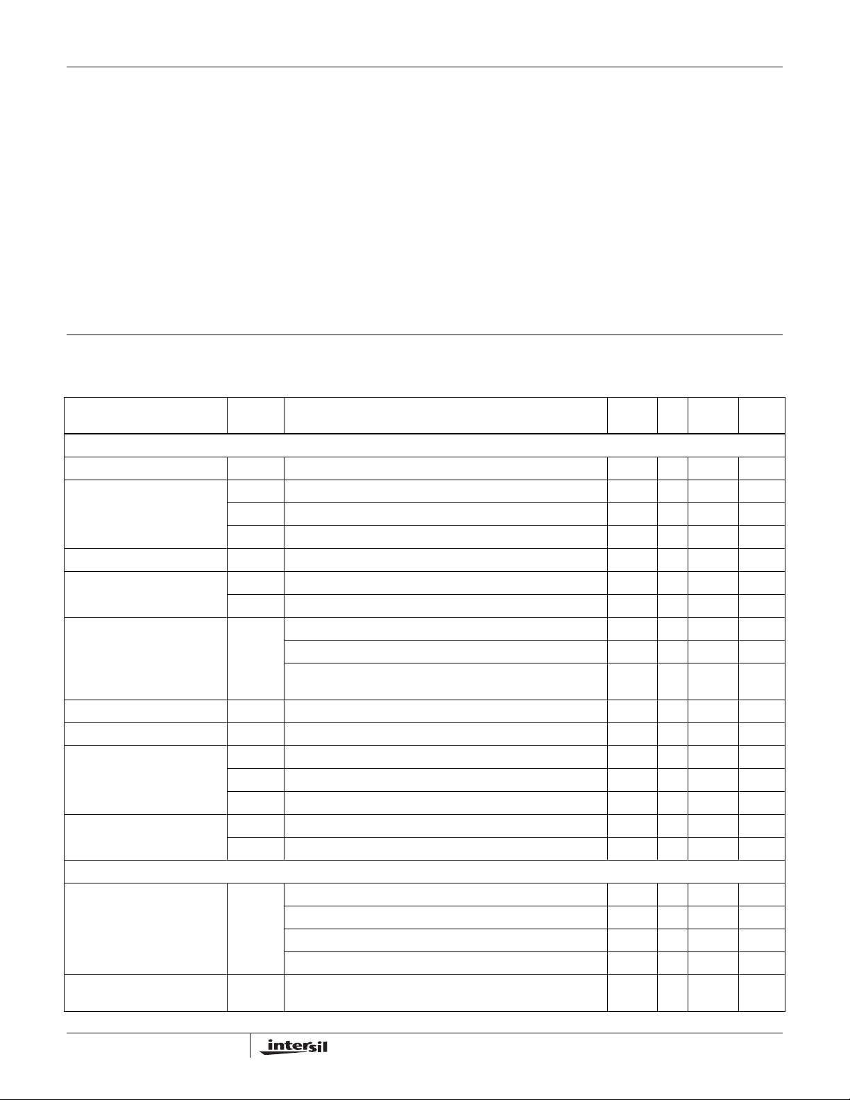
Electrical Specifications Unless otherwise noted, all parameters are guaranteed over the operational supply voltage and temperature
range of the device as follows:
= -40°C to +85°C; VIN = (VO + 0.5V) to 6.5V with a minimum VIN of 2.3V; CIN = 1µF; CO = 1µF;
T
A
= 0.01µF; C
C
BYP
PARAMETER SYMBOL TEST CONDITIONS
DC CHARACTERISTICS
Supply Voltage V
Ground Current Quiescent condition: I
Shutdown Current I
UVLO Threshold V
Regulation Voltage Accuracy Initial accuracy at V
Maximum Output Current I
Internal Current Limit I
Dropout Voltage (Note 7) V
Thermal Shutdown
Temperature
AC CHARACTERISTICS
Ripple Rejection (Note 6) I
Output Noise Voltage (Note 6) I
IN
I
DD1
I
DD2
DDS
UV+
V
UV-
MAX
LIM
DO1IO
V
DO2IO
V
DO3IO
T
SD+
T
SD-
One LDO active 25 32 µA
Both LDO active 42 52 µA
@ +25°C 0.1 1.0 µA
= VO + 0.5V to 5.5V, IO = 10µA to 300mA, TJ = +25°C -0.8 +0.8 %
V
IN
= VO + 0.5V to 5.5V, IO = 10µA to 300mA, TJ = -40°C to
V
IN
+125°C
Continuous 300 mA
= 300mA; VO < 2.5V 300 500 mV
= 300mA; 2.5V ≤ VO ≤ 2.8V 250 400 mV
= 300mA; VO > 2.8V 200 325 mV
= 10mA, VIN = 2.8V(min), VO = 1.8V, C
O
@ 1kHz 90 dB
@ 10kHz 70 dB
@ 100kHz 50 dB
= 100µA, VO = 1.5V, TA = +25°C, C
O
BW = 10Hz to 100kHz
POR
= 0.01µF.
IN
MIN
(Note 8) TYP
2.3 6.5 V
= 0µA; IO2 = 0µA
O1
1.9 2.1 2.3 V
1.6 1.8 2.0 V
= VO + 0.5V, IO = 10mA, TJ = +25°C -0.7 +0.7 %
-1.8 +1.8 %
350 475 600 mA
= 0.1µF
BYP
= 0.1µF
BYP
(°C/W) θJC (°C/W)
JA
MAX
(Note 8) UNITS
145 °C
110 °C
30 µV
RMS
3
FN6391.1
March 11, 2008

ISL9000A
www.BDTIC.com/Intersil
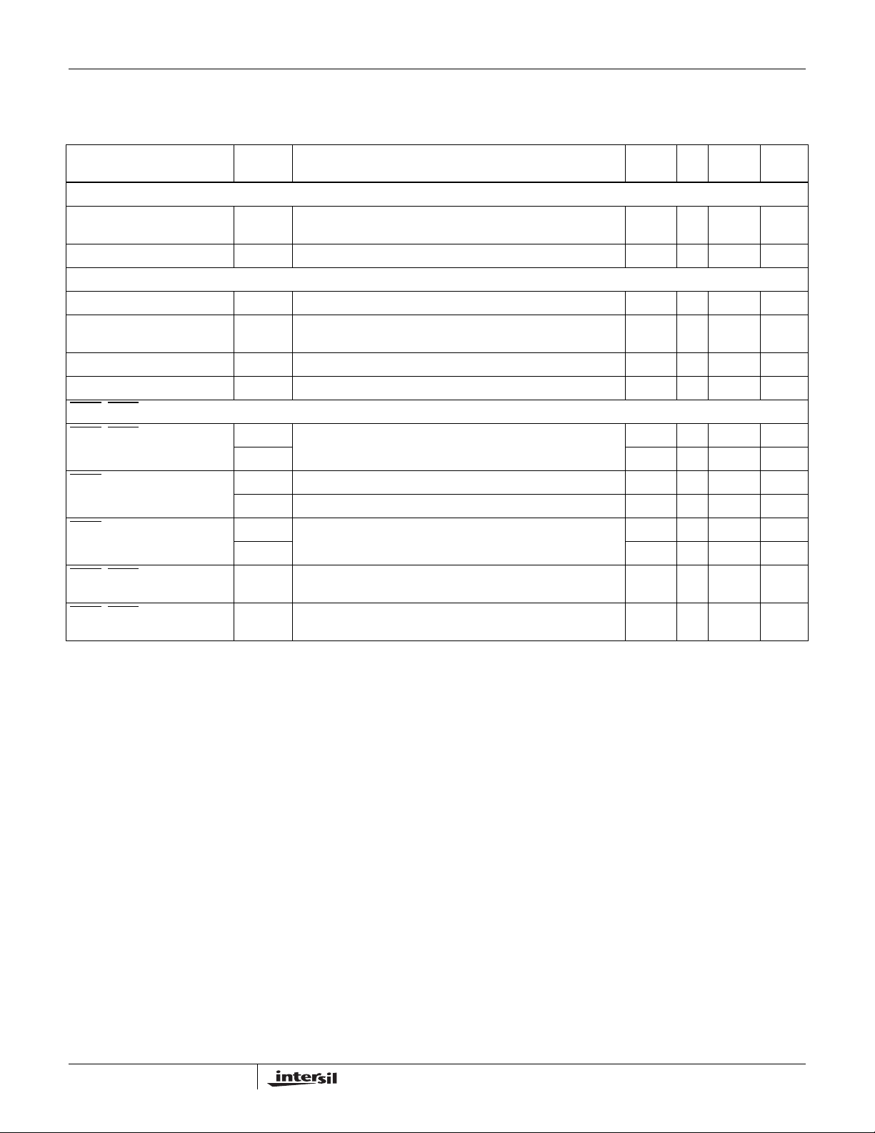
Electrical Specifications Unless otherwise noted, all parameters are guaranteed over the operational supply voltage and temperature
range of the device as follows:
= -40°C to +85°C; VIN = (VO + 0.5V) to 6.5V with a minimum VIN of 2.3V; CIN = 1µF; CO = 1µF;
T
A
= 0.01µF; C
C
BYP
PARAMETER SYMBOL TEST CONDITIONS
DEVICE START-UP CHARACTERISTICS
Device Enable Time t
LDO Soft-Start Ramp Rate t
EN1, EN2 PIN CHARACTERISTICS
Input Low Voltage V
Input High Voltage V
Input Leakage Current I
Pin Capacitance C
, POR2 PIN CHARACTERISTICS
POR1
, POR2 Thresholds V
POR1
POR1
Delay t
Delay t
POR2
, POR2 Pin Output Low
POR1
Voltage
, POR2 Pin Internal
POR1
Pull-Up Resistance
NOTES:
6. Limits established by characterization and are not production tested.
7. VOx = 0.98*VOx(NOM); Valid for VOx greater than 1.85V.
8. Parts are 100% tested at +25°C. Temperature limits established by characterization and are not production tested.
IL
POR+
V
P1LH
t
P1HL
P2LHCPOR
t
P2HL
V
R
Time from assertion of the ENx pin to when the output voltage
EN
reaches 95% of the VO(nom)
Slope of linear portion of LDO output voltage ramp during start-up 30 60 µs/V
SSR
IL
IH
, I
IH
Informative 5 pF
PIN
As a percentage of nominal output voltage 91 94 97 %
POR-
@ IOL = 1.0mA 0.2 V
OL
POR
= 0.01µF. (Continued)
POR
MIN
(Note 8) TYP
-0.3 0.5 V
1.4 V
87 90 93 %
1.0 2.0 3.0 ms
= 0.01µF 100 200 300 ms
78 100 180 kΩ
MAX
(Note 8) UNITS
250 500 µs
+
IN
0.3
0.1 µA
25 µs
25 µs
V
4
FN6391.1
March 11, 2008
 Loading...