

Page 1
ISL9000A Evaluation Board User Guide
Application Note 1767
Description
The ISL9000A Evaluation Board is designed to provide a
complete platform for demonstrating the performance of the
ISL9000A Low Dropout Regulator IC (LDO). It is designed to
show the small space required for all the components, while
providing room to access the signals.
The layout is intended to minimize thermal effects, to better
evaluate current limits and voltage regulation accuracy. In an
actual implementation, the area for heat sinking may be
smaller, so thermal effects may make the operation slightly
different.
The ISL9000A evaluation board constitutes a complete dual
voltage regulator solution. The PCB board is 2 inches by 3
inches, however, the actual charger components easily fit
within a 0.9x1.6 cm area (components on one side),
demonstrating the space saving advantage of the ISL9000A in
limited space applications.
A voltage source can be connected to the two pin connector
(J2, default) or to the banana jacks (not populated). For
monitoring the output, test instruments can be connected to
the five pin connector (J13, default) or to the banana jacks or
scope probe jacks (not populated). Additional test points
provide a convenient way to monitor the POR outputs and the
signal on the bypass capacitor. This can be especially
important when testing the LDO in a temperature chamber.
Several ground pins provide reference points for test leads.
Additional “kelvin” test points are provided for VIN, VO1, VO2,
and GND to monitor the actual performance of the IC. This
removes the voltage drops across the PCB traces that occurs
at higher currents.
The board has a jumper block for enabling each of the two LDO
outputs. A shunt can be placed on J3 or J4 between “ENx” and
“LOW” pins to provide a 100kΩ pull-down on each EN pin of
the device. If J3 or J4 ”HI” pins are floating, the respective LDO
output will be off, while connecting “HI” to “ENx” will enable
the output.
When it is desired that an LDO always be enabled, connect a
shunt between “ENx” and “HI” on J3 or J4. In this case the
shunt between “ENx” and “LOW” is not needed.
If an external enable signal that drives both high and low is
used to enable the LDO outputs, both shunts can be removed
from ENx.
A jumper (J10) connects the CPOR input to a 10nF capacitor
for POR timing. The jumper can be removed and replaced by a
different capacitor to ground for different power on timing
requirements.
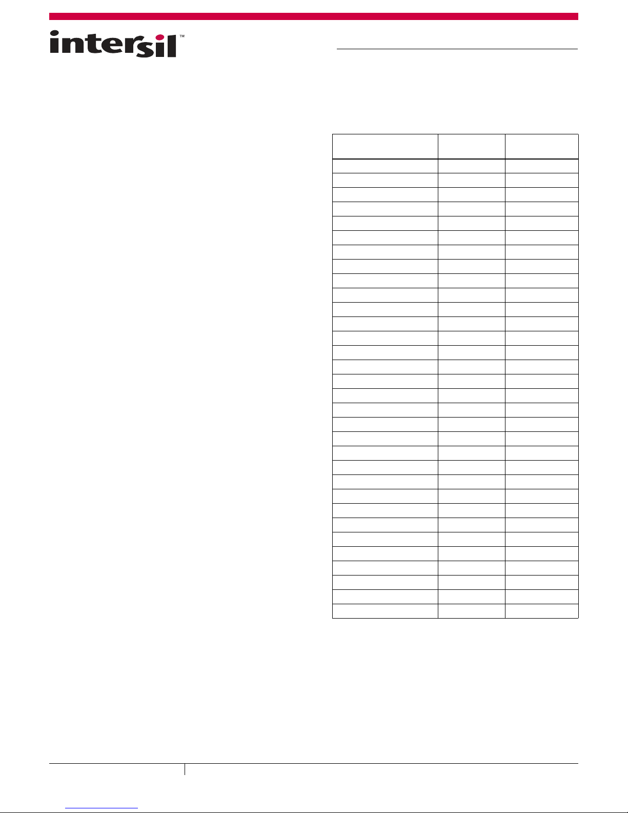
Ordering Information
PART
NUMBER
ISL9000AIRNNZ-EVZ 3.3 3.3
ISL9000AIRNJZ-EVZ 3.3 2.8
ISL9000AIRNFZ-EVZ 3.3 2.5
ISL9000AIRNCZ-EVZ 3.3 1.8
ISL9000AIRMNZ-EVZ 3.0 3.3
ISL9000AIRMMZ-EVZ 3.0 3.0
ISL9000AIRMGZ-EVZ 3.0 2.7
ISL9000AIRLLZ-EVZ 2.9 2.9
ISL9000AIRKNZ-EVZ 2.85 3.3
ISL9000AIRKKZ-EVZ 2.85 2.85
ISL9000AIRKJZ-EVZ 2.85 2.8
ISL9000AIRKFZ-EVZ 2.85 2.5
ISL9000AIRKPZ-EVZ 2.85 1.85
ISL9000AIRKCZ-EVZ 2.85 1.8
ISL9000AIRJNZ-EVZ 2.8 3.3
ISL9000AIRJMZ-EVZ 2.8 3.0
ISL9000AIRJRZ-EVZ 2.8 2.6
ISL9000AIRJCZ-EVZ 2.8 1.8
ISL9000AIRJBZ-EVZ 2.8 1.5
ISL9000AIRGPZ-EVZ 2.7 1.85
ISL9000AIRGCZ-EVZ 2.7 1.8
ISL9000AIRFJZ-EVZ 2.5 2.8
ISL9000AIRFDZ-EVZ 2.5 2.0
ISL9000AIRFCZ-EVZ 2.5 1.8
ISL9000AIRPLZ-EVZ 1.85 2.9
ISL9000AIRPPZ-EVZ 1.85 1.85
ISL9000AIRCJZ-EVZ 1.8 2.8
ISL9000AIRCCZ-EVZ 1.8 1.8
ISL9000AIRBLZ-EVZ 1.5 2.9
ISL9000AIRBJZ-EVZ 1.5 2.8
ISL9000AIRBCZ-EVZ 1.5 1.8
ISL9000AIRBBZ-EVZ 1.5 1.5
The board also provides a connector (JP1, not populated)
which can connect to a logic analyzer/pattern generator for
controlling and monitoring the output response. The connector
provides both enable inputs and POR outputs.
Finally, a daughter card connector and a jumper (J14 and J9,
not populated) allow specially assembled boards containing
untrimmed LDOs to be programmed to custom voltage levels
after board assembly. This is done at the factory, so no
additional information will be provided in this document.
VO1 VOLTAGE
(V)
VO2 VOLTAGE
(V)
June 27, 2012
AN1767.0
1
1-888-INTERSIL or 1-888-468-3774
CAUTION: These devices are sensitive to electrostatic discharge; follow proper IC Handling Procedures.
| Intersil (and design) is a trademark owned by Intersil Corporation or one of its subsidiaries.
All other trademarks mentioned are the property of their respective owners.
Copyright Intersil Americas Inc. 2012. All Rights Reserved.
Page 2

Features
Application Note 1767
• Complete dual low dropout regulator (LDO)
• Easy to use board for evaluation of the LDO in a target
application
• Exposed soldering pads/pins for monitoring VIN, VO1, VO2,
POR1, POR2, and CBYP
• Voltage monitoring using test pins, banana jacks and scope
jacks
• Enable jumpers for each supply, plus jumpered enable
pull-down resistors
• The board has options for:
-Changing the CPOR capacitor
- Using a logic analyser/pattern generator to monitor
enable/POR response
What is Inside
The Evaluation Kit contains:
• ISL9000A Evaluation board
• ISL9000A Data Sheet
• ISL9000A Evaluation Board Users Guide (this document)
What is Needed
The following instruments will be needed to perform testing (not
provided):
• DC 6.5V/1A Power supply
• Two Digital Voltmeters (4.5 digit or better)
• Oscilloscope
• 2 channel, 0 to 400mA electronic load
• Cables and wires
Step 5: Connect a third voltmeter to the input. This can be
connected to the J2 terminal, but at higher inputs, the VIk
terminal will give the most accurate reading of the
voltage at the ISL9000A VIN pin.
Step 6: (Optional) Connect an electronic load to one or both of
the outputs. For the VO1 output, use the VO1 power
connector J2-2 (“V1P”). For the VO2 output, use the VO2
power connector J2-4 (“V2P”).
Step 7: Monitor VO1 and VO2. The voltages should reflect the
voltage of the selected part. For example, the
ISL9000AIRNJZ-EVZ
outputs.
Step 8: Change the loading on each output and monitor the
output voltages
Step 9: Change the input voltage and monitor the effect on the
output voltages
For additional testing, such as load transient and line transient
response, adding the optional scope jacks will improve the
measurement, by reducing external noise. The Scope Jack part
number is included in the bill of materials as an optional
component.
If desired, banana jacks can be added to the board to facilitate
connection of the board to test equipment. Part numbers for
these optional components are included in the bill of materials.
Improved PSRR and noise specs can be obtained by replacing
the 0.01μF (C3) capacitor with a 0.1μF capacitor.
board should have 3.3V and 2.8V
Quick Setup Guide
Step 1: Place shunts on J3 between “EN1” and HI”, on J4
between “EN1” and HI”, and on J10 (CPOR). This is the
factory default connection.
Step 2: Set the power supply to 3.8V with a 1.0A current limit
(then turn off).
Step 3: Connect the power supply between VIN and GND using
connector J2.
Step 4: Connect two voltmeter positive leads to the VO1 “kelvin”
connector (J13-1, “V1K”) and the VO2 “kelvin” connector
(J13-5, “V2K”). The meters can also be connected to the
VO power pins J2-2 and J2-4 or the banana jacks, but at
higher currents, these won’t reflect the output voltage as
accurately as the kelvin connections.
Connect the negative leads to GND J13-3. (To get the best
representation of the IC output voltage under all output
loading conditions, add a ground terminal to the GNDk
pad and connect the meter ground leads there).
2
AN 1767.0
June 27, 2012
Page 3
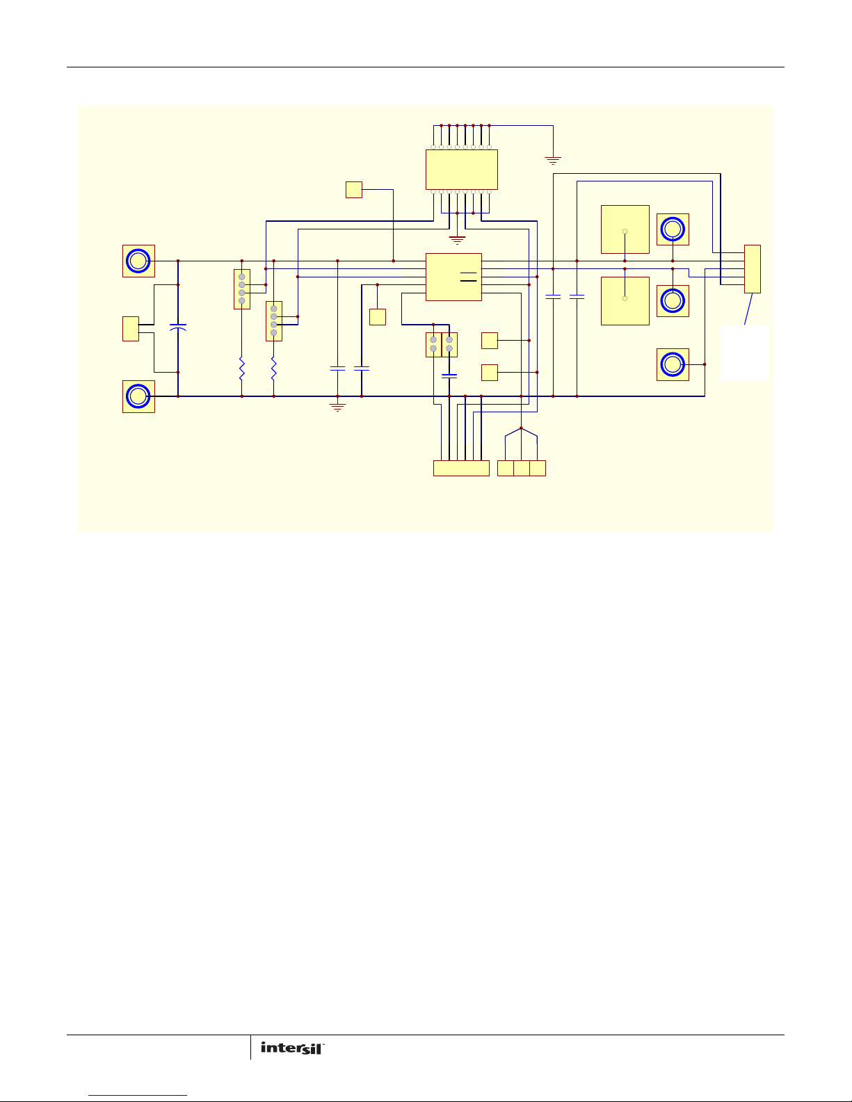
Schematic
VIN
1
EN1
2
EN2
3
CBYP
4
CPOR
5
VO1
10
VO2
9
POR2
8
POR1
7
GND
6
U1
ISL9000
B1
B4
R1
100K
R2
100K
C1
100uF
C2
1uF
C3
0.01uF
J11
SCOPE JACK
J12
SCOPE JACK
B2
B3
1
2
J2
CON2
J10
JMP2
J9
JMP2
C4
0.01uF
12345
6
J14
CON6
1
J6
CON1
1
J8
CON1
1
J5
CON1
J4
JMP4
J3
JMP4
GND
1 2
3 4
5 6
7 8
9 10
11 12
13 14
15 16
JP1
HEADER 8X2
1
J1
CON1
1
J7
CON1
B5
C5
1uFC61uF
1
J15
CON1
1
J16
CON1
1
2
3
4
5
J13
CON5
VO1 - Kelvin
VO1 - Power
GND
VO2 - Power
VO2 - Kelvin
FIGURE 1. ISL9000A EVALUATION BOARD (REV B) SCHEMATIC
Application Note 1767
3
AN 1767.0
June 27, 2012
Page 4
Application Note 1767
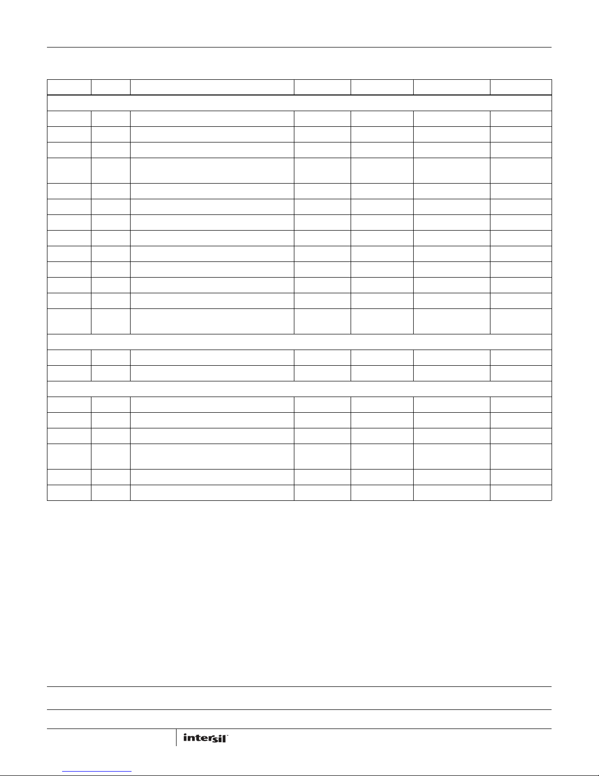
Bill of Materials
ITEM QTY DESCRIPTION DESIGNATOR MFR MFR PART # COMMENTS
COMPONENTS COMMON TO ALL BOARDS
1 1 PCB PCB - ISL9000EV2 REVB
2 2 CAP, SMD, 0603, 0.01µF, 50V, 10%, X7R, ROHS C3, C4 AVX 06035C103KAT2A 0603 capacitor
3 1 CAP, SMD, 0805, 1µF, 16V, 10%, X5R, ROHS C2 Panasonic ECJ-2FB1C105K 0805 capacitor
4 2 CAP, SMD, 1206, 1µF, 25V, 10%, X7R, ROHS C5, C6 Panasonic ECJ-3YB1E105K 1206 or 1210
capacitor
5 2 RES, SMD, 0603, 100kΩ, 1/10W, 1%, ROHS R1, R2 Panasonic ERJ-3EKF1003V 0603 resistor
6 1 CAP-TANTALUM, SMD, 100µF, 16V, 20%, ROHS C1 KEMET T491D107M016AS
7 4 CON1 J1, J5, J7, J16 Keystone 5010
8 3 CON1 J6, J8, J15 Keystone 5016
9 1 CON2 J2 Molex 22-23-2021
10 1 CON5 J13 Molex 22-23-2051
11 1 JMP2 J10 Molex 22-28-4020
12 2 JMP4 J3, J4 Molex 22-28-4040
13 3 Shunt AMP 382811-8 Only 3 needed
per board
COMPONENTS SPECIFIC TO EACH BOARD VARIATION
14 1 ISL9000A U1 Intersil ISL9000AIR_ _Z
15 1 Label L1
COMPONENTS OPTIONAL ON EACH BOARD
16 2 SCOPE JACK J11, J12 Tektronix 131-5031-00 Not populated
17 3 BANANA B1, B2, B3 Keystone 7006 Not populated
18 2 BANANA B4, B5 Keystone 7007 Not populated
19 1 JMP2 J9 Molex 22-28-4020 Not populated
20 1 CON6 J14 HRS DF11-6DS-2DSA Not populated
21 1 HEADER 8X2 JP1 Molex 10-88-1161 Not populated
Intersil Corporation reserves the right to make changes in circuit design, software and/or specifications at any time without notice. Accordingly, the reader is
cautioned to verify that the Application Note or Technical Brief is current before proceeding.
For information regarding Intersil Corporation and its products, see www.intersil.com
4
AN 1767.0
June 27, 2012
 Loading...