

®
ISL89410, ISL89411, ISL89412
Data Sheet July 1, 2009
High Speed, Dual Channel Power
MOSFET Drivers
The ISL89410, ISL89411, ISL89412 ICs are similar to the
EL7202, EL7212, EL7222 series but with greater VDD
ratings. These are very high speed matched dual drivers
capable of delivering peak currents of 2.0A into highly
capacitive loads. The high speed performance is achieved
by means of a proprietary “Turbo-Driver” circuit that speeds
up input stages by tapping the wider voltage swing at the
output. Improved speed and drive capability are enhanced
by matched rise and fall delay times. These matched delays
maintain the integrity of input-to-output pulse-widths to
reduce timing errors and clock skew problems. This
improved performance is accompanied by a 10-fold
reduction in supply currents over bipolar drivers, yet without
the delay time problems commonly associated with CMOS
devices. Dynamic switching losses are minimized with
non-overlapped drive techniques.
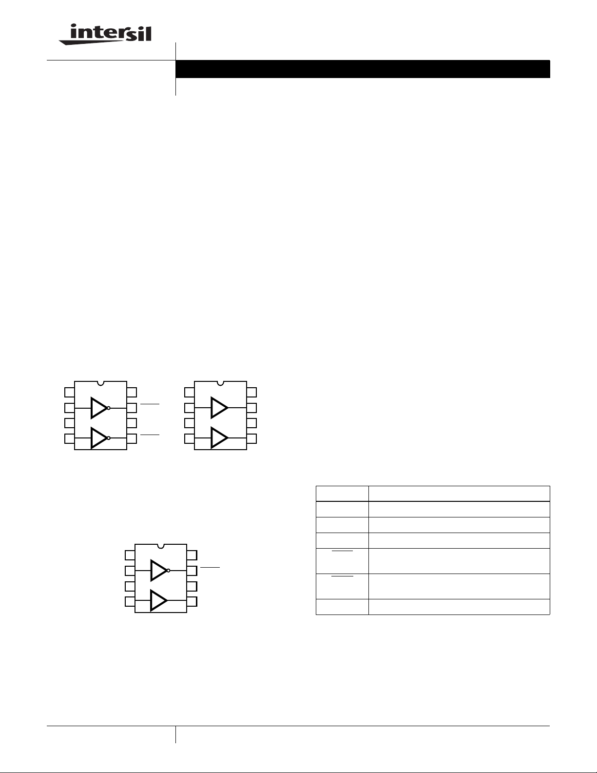
Pinouts
ISL89410
(8 LD PDIP, SOIC)
TOP VIEW
1
2
3
4
8
7
6
5
NC
OUTA
V+
OUTB
(8 LD PDIP, SOIC)
NC
1
2
INA
3
GND
4
INB
ISL89411
TOP VIEW
8
7
6
5
NC
OUTA
V+
OUTB
NC
INA
GND
INB
FN6798.1
Features
• Industry Standard Driver Replacement
• Improved Response Times
• Matched Rise and Fall Times
• Reduced Clock Skew
• Low Output Impedance
• Low Input Capacita n c e
• High Noise Immunity
• Improved Clocking Rate
• Low Supply Current
• Wide Operating Voltage Range
• Pb-Free Available (R oHS compliant)
Applications
• Clock/line Drivers
• CCD Drivers
• Ultra-Sound Transducer Drivers
• Power MOSFET Drivers
• Switch Mode Power Supplies
• Class D Switching Amplifiers
• Ultrasonic and RF Generators
INVERTING
DRIVERS
ISL89412
(8 LD PDIP, SOIC)
TOP VIEW
NC
1
2
INA
3
GND
4
INB
COMPLEMENTARY
DRIVERS
Manufactured under U.S. Patent Nos. 5,334,883, #5,341,047
1
NON-INVERTING
DRIVERS
8
NC
7
OUTA
6
v+
5
OUTB
1-888-INTERSIL or 1-888-468-3774
• Pulsed Circuits
Pin Descriptions
SYMBOL PIN DESCRIPTIONS
V
GND Power voltage return
INA, INB Logic inputs.
OUTA
OUTA
OUTB
OUTB
NC These pins must be left unconnected.
CAUTION: These devices are sensitive to electrostatic discharge; follow proper IC Handling Procedures.
Power voltage from 4.5V to 18V.
+
Non-inverted ouput for ISL89410. Inverted output
for ISL89411 and ISL89412.
Non-inverted output for ISL89410 and ISL89412.
Inverted output for ISL89411.
| Intersil (and design) is a registered trademark of Intersil Americas Inc.
Copyright Intersil Americas Inc. 2008, 2009. All Rights Reserved
All other trademarks mentioned are the property of their respective owners.
Ordering Information
ISL89410, ISL89411, ISL89412
PART
NUMBER
ISL89410IP ISL 89410IP -40 to +85 8 Ld PDIP E8.3
ISL89410IPZ (Note) 89410 IPZ -40 to +85 8 Ld PDIP** (Pb-free) E8.3
ISL89410IBZ (Note) 89410 IBZ -40 to +85 8 Ld SOIC (Pb-free) MDP0027
ISL89410IBZ-T13* (Note) 89410 IBZ -40 to +85 8 Ld SOIC (Tape and Reel)
ISL89411IP ISL 89411IP -40 to +85 8 Ld PDIP E8.3
ISL89411IPZ (Note) ISL 89411IPZ -40 to +85 8 Ld PDIP** (Pb-free) E8.3
ISL89411IBZ (Note) 89411 IBZ -40 to +85 8 Ld SOIC (Pb-free) MDP0027
ISL89411IBZ-T13* (Note) 89411 IBZ -40 to +85 8 Ld SOIC (Tape and Reel)
ISL89412IP ISL 89412IP -40 to +85 8 Ld PDIP E8.3
ISL89412IPZ 89412 IPZ -40 to +85 8 Ld PDIP** (Pb-free) E8.3
ISL89412IBZ (Note) 89412 IBZ -40 to +85 8 Ld SOIC (Pb-free) MDP0027
ISL89412IBZ-T13* (Note) 89412 IBZ -40 to +85 8 Ld SOIC (Tape and Reel)
*Please refer to TB347 for details on reel specifications.
**Pb-free PDIPs can be used for through-hole wave solder processing only. They are not intended for use in Reflow solder processing applications
NOTE: These Intersil Pb-free plastic packaged products employ special Pb-free material sets, molding compounds/die attach materials, and 100%
matte tin plate plus anneal (e3 termination finish, which is RoHS compliant and compatible with both SnPb and Pb-free soldering operations). Intersil
Pb-free products are MSL classified at Pb-free peak reflow temperatures that meet or exceed the Pb-free requirements of IPC/JEDEC J STD-020.
PART
MARKING
TEMP. RANGE
(°C) PACKAGE
(Pb-free)
(Pb-free)
(Pb-free)
PKG.
DWG. #
MDP0027
MDP0027
MDP0027
2
FN6798.1
July 1, 2009
ISL89410, ISL89411, ISL89412
Absolute Maximum Ratings Thermal Information
Supply (V+ to GND). . . . . . . . . . . . . . . . . . . . . . . . . . . . . . . . . 19.0V
Input Pins. . . . . . . . . . . . . . . . . . . . . . . . . . -0.3V to +0.3V above V+
Combined Peak Output Current. . . . . . . . . . . . . . . . . . . . . . . . . . .4A
Maximum Recommended Operating Conditions
Recommended Operating V+ Range. . . . . . . . . . . . . . 4.5V to 18.0V
Input Pins. . . . . . . . . . . . . . . . . . . . . . . . . . . . . . . . . . . . . . .0V to V+
CAUTION: Do not operate at or near the maximum ratings listed for extended periods of time. Exposure to such conditions may adversely impact product reliability and
result in failures not covered by warranty.
Operating Junction Temperature . . . . . . . . . . . . . . . . . . . . . .+125°C
Power Dissipation
8 Ld SOIC . . . . . . . . . . . . . . . . . . . . . . . . . . . . . . . . . . . . .570mW
8 Ld PDIP* . . . . . . . . . . . . . . . . . . . . . . . . . . . . . . . . . . . .1050mW
Storage Temperature Range . . . . . . . . . . . . . . . . . .-65°C to +150°C
Ambient Operating Temperature . . . . . . . . . . . . . . . .-40°C to +85°C
Pb-Free Reflow Profile. . . . . . . . . . . . . . . . . . . . . . . . .see link below
http://www.intersil.com/pbfree/Pb-FreeReflow.asp
*Pb-free PDIPs can be used for through-hole wave solder
processing only. They are not intended for use in Reflow solder
processing applications.
IMPORTANT NOTE: All parameters having Min/Max specifications are guaranteed. Typical values are for information purposes only. Unless otherwise noted, all tests
are at the specified temperature and are pulsed tests, therefore: T
DC Electrical Specifications T
= +25°C, V = 18V unless otherwise specified; Parameters with MIN and/or MAX limits are 100% tested
A
= TC = T
J
A
at +25°C, unless otherwise specified. Temperature limits established by characterization and are not
production tested.
PARAMETER DESCRIPTION TEST CONDITIONS MIN TYP MAX UNITS
INPUT
V
I
IH
V
I
IL
V
IH
IL
HVS
Logic “1” Input Voltage 2.4 V
Logic “1” Input Current @V+ 0.1 10 µA
Logic “0” Input Voltage 0.8 V
Logic “0” Input Current @0V 0.1 10 µA
Input Hysteresis 0.3 V
OUTPUT
R
OH
R
OL
I
PK
Pull-Up Resistance I
Pull-Down Resistance I
Peak Output Current Source 2 A
= -100mA 3 6 Ω
OUT
= +100mA 4 6 Ω
OUT
Sink 2 A
I
DC
Continuous Output Current Source/Sink 100 mA
POWER SUPPLY
I
S
Power Supply Current Inputs High/ISL89410 4.5 7.5 mA
Inputs High/ISL89411 1 2.5 mA
Inputs High/ISL89412 2.5 5.0 mA
V
S
Operating Voltage 4.5 18 V
AC Electrical Specifications T
= +25°C, V = 18V unless otherwise specified.
A
PARAMETER DESCRIPTION TEST CONDITIONS MIN TYP MAX UNITS
SWITCHING CHARACTERISTICS
t
R
t
F
t
D1
t
D2
Rise Time (Note 1) CL = 500pF 7.5 ns
= 1000pF 10 20 ns
C
L
Fall Time (Note 1) CL = 500pF 10 ns
= 1000pF 13 20 ns
C
L
Turn-On Delay Time (Note 1) See “Timing Table” on page 4 18 25 ns
Turn-Off Delay Time (Note 1) See“Timing Table” on page 4 20 25 ns
NOTE:
1. Limits established by characterization and are not production tested.
3
FN6798.1
July 1, 2009

Timing Table
ISL89410, ISL89411, ISL89412
5V
INPUT 2.5V
0
NON-INVERTED
Standard Test Configuration
INVERTED
OUTPUT
OUTPUT
90%
10%
90%
10%
V+
INPUT
2
t
D1
46
t
4.7µF
TAN+
OUTPUT
1000pF
D2
t
R
t
F
t
F
t
R
7
Simplified Schematic
V+
INPUT
INPUT
BUFFER
+
-
+
V
REF
-
REFERENCE
AND LEVEL
SHIFTER
3
INVERTING
BUFFER
WITH
HYSTERESIS
2ND
INVERTING
BUFFER
SUPER
INVERTER
OUTPUT
4
FN6798.1
July 1, 2009

Typical Performance Curves
FIGURE 1. MAX POWER/DERATING CURVES FIGURE 2. SWITCH THRESHOLD vs SUPPLY VOLTAGE
ISL89410, ISL89411, ISL89412
FIGURE 3. INPUT CURRENT vs VOLTAGE
FIGURE 5. QUIESCENT SUPPLY CURRENT
5
FIGURE 4. PEAK DRIVE vs SUPPLY VOLTAGE
ISL89410
ISL89411
ISL89412
FN6798.1
July 1, 2009

ISL89410, ISL89411, ISL89412
Typical Performance Curves (Continued)
FIGURE 6. “ON” RESISTANCE vs SUPPLY VOLTAGE
FIGURE 8. AVERAGE SUPPL Y CURRENT vs CAP ACITIVE
LOAD
FIGURE 7. AVERAGE SUPPLY CURRENT vs VOLTAGE AND
FREQUENCY
FIGURE 9. RISE/FALL TIME vs LOAD
FIGURE 10. RISE/FALL TIME vs SUPPLY VOLTAGE
6
FIGURE 11. PROPAGATION DELAY vs SUPPLY VOLTAGE
FN6798.1
July 1, 2009

ISL89410, ISL89411, ISL89412
Typical Performance Curves (Continued)
FIGURE 12. RISE/FALL TIME vs TEMPERATURE FIGURE 13. DELAY vs TEMPERATURE
ISL89411 Macro Model
**** ISL89411 Model ****
* input
* | gnd
* | | Vsupply
* | | | Vout
.subckt M89411 2 3 6 7
V1 12 3 1.6
R1 13 15 1k
R2 14 15 5k
R5 11 12 100
C1 15 3 43.3 pF
D1 14 13 dmod
X1 13 11 2 3 comp1
X2 16 12 15 3 comp1
sp 6 7 16 3 spmod
sn 7 3 16 3 snmod
g1 11 0 13 0 938µ
.model dmod d
.model spmod vswitch ron3 roff2meg von1 voff1.5
.model snmod vswitch ron4 roff2meg von3 voff2
.ends M89411
7
FN6798.1
July 1, 2009

ISL89410, ISL89411, ISL89412
.subckt comp1 out inp inm vss
e1 out vss table { (v(inp) v(inm))* 5000} (0,0) (3.2,3.2)
Rout out vss 10meg
Rinp inp vss 10meg
Rinm inm vss 10meg
.ends comp1
Application Guidelines
It is important to minimize inductance to the power FET by
keeping the output drive current loop as short as possible.
Also, the decoupling capacitor, Cq, should be a high quality
ceramic capacitor with a Q that should be a least 10x the
gate Q of the power FET. A ground plane under this circuit is
also recommended.
V+
Cq SHOULD BE AS CLOSE AS
POSSIBLE TO THE V+ AND
GND PINS
C
q
LOOP AS
SHORT AS
POSSIBLE
V+
C
q
GND
FIGURE 15. SUGGESTED CONFIGURATION FOR DRIVING
INDUCTIVE LOADS
PARASITIC LEAD
INDUCTANCE
Where high supply voltage operation is required (15V to
18V), input signals with a minimum of 3.3V input drive is
suggested and a minimum rise/fall time of 100ns. This is
recommended to minimize the internal bias current power
dissipation.
Excessive power dissipation in the driver can result when
driving highly capacitive FET gates at high frequencies.
These gate power losses are defined by Equation 1:
P2QCVgs•• fSW•=
(EQ. 1)
GND
FIGURE 14. RECOMMENDED LAYOUT METHODS
In applications where it is difficult to place the driver very
close to the power FET (which may result with excessive
parasitic inductance), it then may be necessary to add an
external gate resistor to dampen the inductive ring. If this
resistor must be too large in value to be effective, then as an
alternative, Schottky diodes can be added to clamp the ring
voltage to V+ or GND.
where:
P = Power
Q
= Charge of the Power FET at V
c
gs
Vgs = Gate drive voltage (V+)
f
= switching Frequency
SW
Adding a gate resistor to the output of the driver will transfer
some of the driver dissipation to the resisto r. Another
possible solution is to lower the gate driver voltage which
also lowers Q
.
c
8
FN6798.1
July 1, 2009

ISL89410, ISL89411, ISL89412
Small Outline Package Family (SO)
A
D
NN
(N/2)+1
h X 45¬
PIN #1
E
C
SEATING
PLANE
0.004 C
E1
B
0.010 BM CA
I.D. MARK
1
e
0.010 BM CA
(N/2)
c
SEE DETAIL ‚Ä ú
L1
H
A2
GAUGE
PLANE
A1
b
DETAIL X
L
4¬× ¬±
MDP0027
SMALL OUTLINE PACKAGE FAMILY (SO)
INCHES
SO16
SYMBOL
(0.150”)
A 0.068 0.068 0.068 0.104 0.104 0.104 0.104 MAX -
A1 0.006 0.006 0.006 0.007 0.007 0.007 0.007 ±0.003 -
A2 0.057 0.057 0.057 0.092 0.092 0.092 0.092 ±0.002 -
b 0.017 0.017 0.017 0.017 0.017 0.017 0.017 ±0.003 -
c 0.009 0.009 0.009 0.011 0.011 0.011 0.011 ±0.001 -
D 0.193 0.341 0.390 0.406 0.504 0.606 0.704 ±0.004 1, 3
E 0.236 0.236 0.236 0.406 0.406 0.406 0.406 ±0.008 -
E1 0.154 0.154 0.154 0.295 0.295 0.295 0.295 ±0.004 2, 3
e 0.050 0.050 0.050 0.050 0.050 0.050 0.050 Basic -
L 0.025 0.025 0.025 0.030 0.030 0.030 0.030 ±0.009 -
L1 0.041 0.041 0.041 0.056 0.056 0.056 0.056 Basic -
h 0.013 0.013 0.013 0.020 0.020 0.020 0.020 Reference -
N 8 14 16 16 20 24 28 Reference -
NOTES:
1. Plastic or metal protrusions of 0.006” maximum per side are not included.
2. Plastic interlead protrusions of 0.010” maximum per side are not included.
3. Dimensions “D” and “E1” are measured at Datum Plane “H”.
4. Dimensioning and tolerancing per ASME Y14.5M-1994
SO16 (0.300”)
(SOL-16)
SO20
(SOL-20)
SO24
(SOL-24)
SO28
(SOL-28)
TOLERANCE NOTESSO-8 SO-14
A
0.010
Rev. M 2/07
9
FN6798.1
July 1, 2009

ISL89410, ISL89411, ISL89412
Dual-In-Line Plastic Packages (PDIP)
N
D1
-C-
E1
-B-
A2
A
L
A
1
e
C
e
e
INDEX
AREA
BASE
PLANE
SEATING
PLANE
D1
B1
12 3 N/2
-AD
e
B
0.010 (0.25) C AM BS
NOTES:
1. Controlling Dimensions: INCH. In case of conflict between
English and Metric dimensions, the inch dimensions control.
2. Dimensioning and tolerancing per ANSI Y14.5M-1982.
3. Symbols are defined in the “MO Series Symbol List” in Section
2.2 of Publication No. 95.
4. Dimensions A, A1 and L are measured with the package seated
in JEDEC seating plane gauge GS-3.
5. D, D1, and E1 dimensions do not include mold flash or protrusions. Mold flash or protrusions shall not exceed 0.010 inch
(0.25mm).
6. E and are measured with the leads constrained to be per-
7. e
e
pendicular to datum .
A
and eC are measured at the lead tips with the leads uncon-
B
strained. e
must be zero or greater.
C
-C-
8. B1 maximum dimensions do not include dambar protrusions.
Dambar protrusions shall not exceed 0.010 inch (0.25mm).
9. N is the maximum number of terminal positions.
10. Corner leads (1, N, N/2 and N/2 + 1) for E8.3, E16.3, E18.3,
E28.3, E42.6 will have a B1 dimension of 0.030 - 0.045 inch
(0.76 - 1.14mm).
E8.3 (JEDEC MS-001-BA ISSUE D)
8 LEAD DUAL-IN-LINE PLASTIC PACKAGE
INCHES MILLIMETERS
SYMBOL
A - 0.210 - 5.33 4
E
A1 0.015 - 0.39 - 4
A2 0.115 0.195 2.93 4.95 -
B 0.014 0.022 0.356 0.558 -
C
L
A
C
B
B1 0.045 0.070 1.15 1.77 8, 10
C 0.008 0.014 0.204 0.355 -
D 0.355 0.400 9.01 10.16 5
D1 0.005 - 0.13 - 5
E 0.300 0.325 7.62 8.25 6
E1 0.240 0.280 6.10 7.11 5
e 0.100 BSC 2.54 BSC -
e
A
e
B
0.300 BSC 7.62 BSC 6
- 0.430 - 10.92 7
L 0.115 0.150 2.93 3.81 4
N8 89
NOTESMIN MAX MIN MAX
Rev. 0 12/93
All Intersil U.S. products are manufactured, assembled and tested utilizing ISO9000 quality systems.
Intersil Corporation’s quality certifications can be viewed at www.intersil.com/design/quality
Intersil products are sold by description only. Intersil Corporation reserves the right to make changes in circuit design, software and/or specifications at any time without
notice. Accordingly, the reader is cautioned to verify that data sheets are current before placing orders. Information furnished by Intersil is believed to be accurate and
reliable. However, no responsibility is assumed by Intersil or its subsidiaries for its use; nor for any infringements of patents or other rights of third parties which may result
from its use. No license is granted by implicat ion or oth erwise u nde r any p a tent or p at ent r ights of Intersil or its subsidiaries.
For information regarding Intersil Corporation and its products, see www.intersil.com
10
FN6798.1
July 1, 2009
 Loading...