

Intersil ISL 88731A Datasheet
®
ISL88731A
Data Sheet January 7, 2009
SMBus Level 2 Battery Charger
The ISL88731A is a highly integrated Lithium-ion battery
charger controller, programmab le over the SMBus system
management bus (SMBus). The ISL88731A is intended to be
used in a smart battery charger (SBC) within a smart battery
system (SBS) that throttles the charge power such that the
current from the AC-adapter is automatically limited. High
efficiency is achieved with a DC/DC synchronous-rectifier
buck converter, equipped with diode emulati on for enhanced
light load efficiency and system bus boosting prevention. The
ISL88731A charges one to four Lithium-ion series cells, and
delivers up to 8A charge current. Integrated MOSFET
drivers and bootstrap diode result in fewer components and
smaller implementation area. Low offset current-sense
amplifiers provide high accuracy with 10mΩ sense resistors.
The ISL88731A provides 0.5% end-of-charge battery
voltage accuracy.
The ISL88731A provides a digital output that indicates the
presence of the AC-adapter as well as an analog output
which indicates the adapter current within 4% accuracy.
The ISL88731A is available in a small 5mmx5mm 28 Ld thin
(0.8mm) QFN package. An evaluation kit is available to
reduce design time. The ISL88731A is available in Pb-Free
packages.
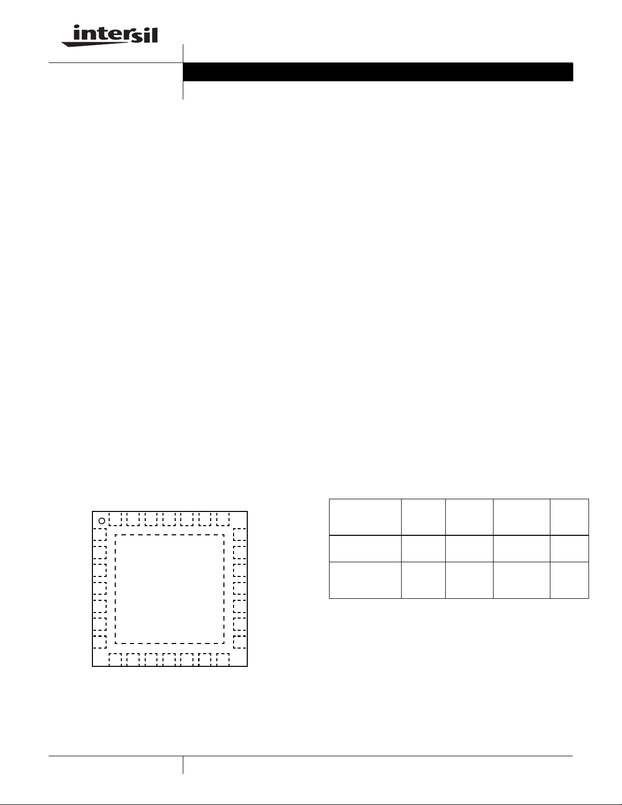
Pinout
ISL88731A
(28 LD TQFN)
TOP VIEW
CSSP
CSSN
VCC
BOOT
UGATE
PHASE
DCIN
28 27 26 25 24 23 22
NC
ACIN
VREF
ICOMP
NC
VCOMP
NC
1
2
3
4
5
6
7
8 9 10 11 12 13 14
ICM
SDA
SCL
VDDSMB
GND
ACOK
NC
21
20
19
18
17
16
15
VDDP
LGATE
PGND
CSOP
CSON
NC
VFB
FN6738.1
Features
• 0.5% Battery Voltage Accuracy
• 3% Adapter Current Limit Accuracy
• 3% Charge Current Accuracy
• SMBus 2 Wire Serial Interface
• Battery Short Circuit Protection
• Fast Response for Pulse-Charging
• Fast System-Load Transient Response
• Monitor Outputs
- Adapter Current (3% Accuracy)
- AC-Adapter Detection
• 11-Bit Battery Voltage Setting
• 6 Bit Charge Current/Adapter Current Setting
• 8A Maximum Battery Charger Current
• 11A Maximum Adapter Current
• +8V to +28V Adapter Voltage Range
• Pb-Free (RoHS compliant)
Applications
• Notebook Computers
• Tablet PCs
• Portable Equipment with Rechargeable Batteries
Ordering Information
PART
NUMBER
(Note)
ISL88731AHRZ ISL887
ISL88731AHRZ-T* ISL887
*Please refer to TB347 for details on reel specifications.
NOTE: These Intersil Pb-free plastic packaged products employ special
Pb-free material sets, molding compounds/die attach materials, and
100% matte tin plate plus anneal (e3 termination finish, which is RoHS
compliant and compatible with both SnPb and Pb-free soldering
operations). Intersil Pb-free products are MSL classified at Pb-free peak
reflow temperatures that meet or exceed the Pb-free requirements of
IPC/JEDEC J STD-020.
PART
MARKING
31AHRZ
31AHRZ
TEMP
RANGE
(°C)
-10 to +100 28 Ld 5x5
-10 to +100 28 Ld 5x5
PACKAGE
(Pb-Free)
TQFN
TQFN (Tape
and Reel)
PKG.
DWG. #
L28.5x5B
L28.5x5B
1
CAUTION: These devices are sensitive to electrostatic discharge; follow proper IC Handling Procedures.
1-888-INTERSIL or 1-888-468-3774
| Intersil (and design) is a registered trademark of Intersil Americas Inc.
Copyright Intersil Americas Inc. 2008, 2009. All Rights Reserved
All other trademarks mentioned are the property of their respective owners.
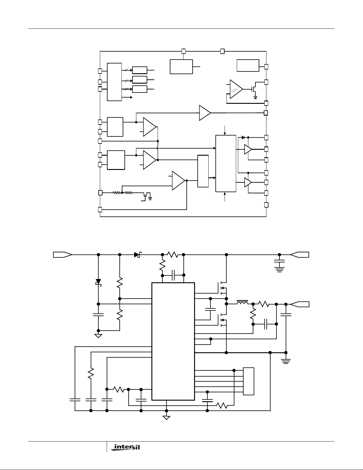
ISL88731A
VDDSMB
SDA
SCL
CSSP
CSSN
IC O MP
CSOP
CSON
VFB
VCOMP
SMBUS
LEVEL
SHIFTER
20x
LEVEL
SHIFTER
20x
500k
11
6
6
100k
EN
DACS
DACI
DACV
DACS
DACI
EN
+
+
GMS
GMI
DACV
DACS
DACI
DACV
DCIN
LINEAR
REGU LATOR
+
GMV
-
BUFF
LVB
VDDP
CSO
LVB
VCC
REF
+
-
EN
DC/DC
CONVERTER
CSSP
REFERENCE
VREF
ACOK
ACIN
IC M
BOOT
UGATE
PHASE
VDDP
LGATE
PGND
GND
AC ADAPTER
AGND
FIGURE 1. FUNCTIONAL BLOCK DIAGRAM
RS1
CSSNCSSP
UGATE
ACIN
DCIN
PHASE
ISL88731A
BOOT
LGATE
CSOP
CSON
ICOMP
VCOMP
VDDP
VREF
VCC
GND
VFB
PGND
ACOK
ICM
SDA
SCL
VDDSMB
TO SYSTEM
RS2
HOST
TO BATTERY
PGND
AGND
FIGURE 2. TYPICAL APPLICATION CIRCUIT
2
FN6738.1
January 7, 2009
ISL88731A
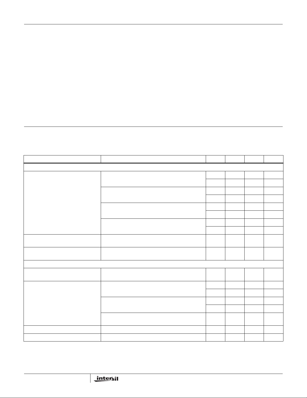
Absolute Maximum Ratings
DCIN, CSSP, CSSN, CSOP, CSON, VFB . . . . . . . . . .-0.3V to +28V
CSSP-CSSN, CSOP-CSON, PGND-GND. . . . . . . . . -0.3V to +0.3V
PHASE to GND . . . . . . . . . . . . . . . . . . . . . . . . . . . . . . . -6V to +30V
BOOT to GND . . . . . . . . . . . . . . . . . . . . . . . . . . . . . . .-0.3V to +33V
BOOT to PHASE . . . . . . . . . . . . . . . . . . . . . . . . . . . . . .-0.3V to +6V
UGATE . . . . . . . . . . . . . . . . . . . . . . .PHASE - 0.3V to BOOT +0.3V
LGATE . . . . . . . . . . . . . . . . . . . . . . . .PGND - 0.3V to VDDP +0.3V
ICOMP, VCOMP, VREF, to GND . . . . . . . . . . . . -0.3V to VCC +0.3V
VDDSMB, SCL, SDA, ACIN, ACOK . . . . . . . . . . . . . . .-0.3V to +6V
VDDP, ICM, VCC to GND, VDDP to PGND. . . . . . . . . .-0.3V to +6V
CAUTION: Do not operate at or near the maximum ratings listed for extended periods of time. Exposure to such conditions may adversely impact product relia bility and
result in failures not covered by warranty.
NOTES:
is measured with the component mounted on a highly effective thermal conductivity test board on free air. See T ech Brief TB379 for det ails.
1. θ
JA
2. For θ
, the “case temp” location is the center of the exposed metal pad on the package underside.
JC
Thermal Information
Thermal Resistance (Typical, Notes 1, 2) θJA (°C/W) θJC (°C/W)
QFN Package. . . . . . . . . . . . . . . . . . . . 39 9.5
Junction Temperature Range. . . . . . . . . . . . . . . . . .-55°C to +150°C
Operating Temperature Range . . . . . . . . . . . . . . . .-10°C to +100°C
Storage Temperature . . . . . . . . . . . . . . . . . . . . . . . .-65°C to +150°C
Pb-Free Reflow Profile. . . . . . . . . . . . . . . . . . . . . . . . .see link below
http://www.intersil.com/pbfree/Pb-FreeReflow.asp
Electrical Specifications DCIN = CSSP = CSSN = 18V, CSOP = CSON = 12V, VDDP = 5V, BOOT-PHASE = 5.0V, GND = PGND = 0V,
CVDDP = 1µF, IVDDP = 0mA, T
at +25°C, unless otherwise specified. T emperature limits est ablished by characterization and are not production
tested.
PARAMETER CONDITIONS MIN TYP MAX UNITS
CHARGE VOLTAGE REGULATION
Battery Full Charge Voltage and Accuracy ChargeVoltage = 0x41A0 16.716 16.8 16.884 V
ChargeVoltage = 0x3130 12.529 12.592 12.655 V
ChargeVoltage = 0x20D0 8.350 8.4 8.450 V
ChargeVoltage = 0x1060 4.163 4.192 4.221 V
Battery Undervoltage Lockout Trip Point
for Trickle Charge
Battery Undervoltage Lockout Trip Point
Hysteresis
CHARGE CURRENT REGULATION
CSOP to CSON Full-Scale Current-Sense
Voltage
Charge Current and Accuracy RS2 = 10mΩ (see Figure 2)
Charge Current Gain Error Based on charge current = 128mA and 8.064A -1.6 1.4 %
CSOP/CSON Input Voltage Range 0 19 V
VFB rising 2.55 2.7 2.85 V
ChargingCurrent = 0x1f80
RS2 = 10mΩ (see Figure 2)
ChargingCurrent = 0x0f80
RS2 = 10mΩ (see Figure 2)
ChargingCurrent = 0x0080
= -10°C to +100°C. Parameters with MIN and/or MAX limits are 100% tested
A
-0.5 0.5 %
-0.5 0.5 %
-0.6 0.6 %
-0.7 0.7 %
100 250 400 mV
78.22 80.64 83.06 mV
7.822 8.064 8.306 A
-3 3 %
3.809 3.968 4.126 A
-4 4 %
64 128 220 mA
3
FN6738.1
January 7, 2009
ISL88731A
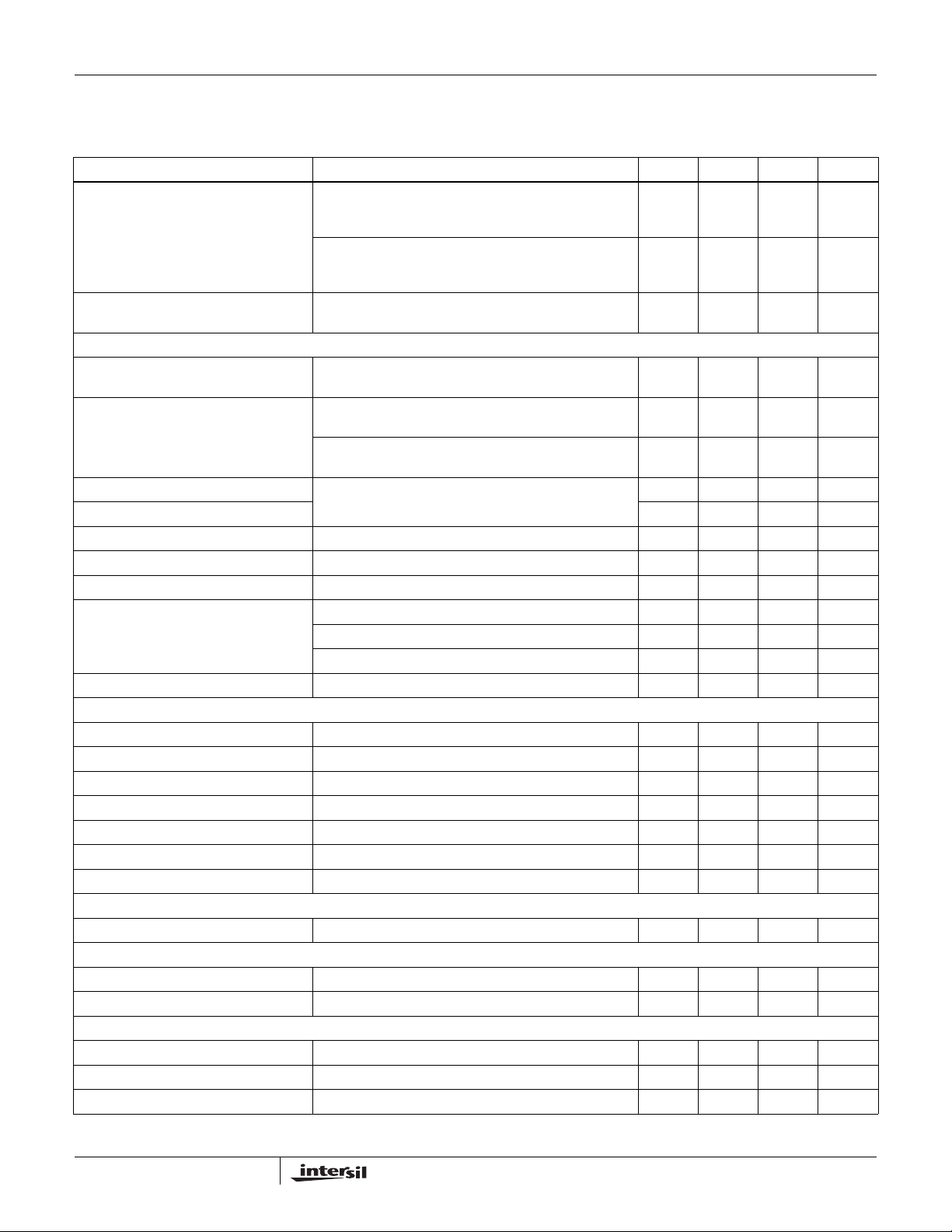
Electrical Specifications DCIN = CSSP = CSSN = 18V, CSOP = CSON = 12V, VDDP = 5V, BOOT-PHASE = 5.0V, GND = PGND = 0V,
CVDDP = 1µF, IVDDP = 0mA, T
at +25°C, unless otherwise specified. T emperature limits est ablished by characterization and are not production
tested. (Continued)
PARAMETER CONDITIONS MIN TYP MAX UNITS
Battery Quiescent Current Adapter present, not charging,
I
CSOP
V
PHASE
+ I
CSON
= V
+ I
CSON
Adapter Absent
I
Adapter Quiescent Current I
+ I
CSOP
V
PHASE
DCIN+ICSSP+ICSSN
V
ADAPTER
+ I
CSON
= V
CSON
= 8V to 26V, V
INPUT CURRENT REGULATION
CSSP to CSSN Full-Scale Current-Sense
CSSP = 19V 106.7 110 113.3 mV
Voltage
Input Current Accuracy RS1 = 10mΩ (see Figure 2)
Adapter Current = 11004mA or 3584mA
RS1 = 10mΩ (see Figure 2)
Adapter Current = 2048mA
Input Current Limit Gain Error Based on InputCurrent = 1024mA and 11004mA -1.5 1.5 %
Input Current Limit Offset -1 1 mV
CSSP/CSSN Input Voltage Range 826V
ICM Gain V
CSSP-CSSN
ICM Offset Based on V
ICM Accuracy V
ICM Max Output Current V
CSSP-CSSN
V
CSSP-CSSN
V
CSSP-CSSN
CSSP-CSSN
= 110mV 19.8 20 20.2 V/V
CSSP-CSSN
= 110mV -2.5 2.5 %
= 55mV or 35mV -4 4 %
= 20mV -8 8 %
= 0.1V 500 µA
SUPPLY AND LINEAR REGULATOR
DCIN, Input Voltage Range 826V
VDDP Output Voltage 8.0V < V
VDDP Load Regulation 0 < I
VDDP
< 28V, no load 4.9 5.1 5.3 V
DCIN
< 30mA 35 100 mV
VDDSMB Range 2.7 5.5 V
VDDSMB UVLO Rising 2.4 2.5 2.6 V
VDDSMB UVLO Hysteresis 100 150 200 mV
VDDSMB Quiescent Current VDDP = SCL = SDA = 5.5V 20 27 µA
V REFERENCE
VREF Output Voltage 0 < I
< 300µA 3.1 3.2 3.3 V
VREF
ACOK
ACOK Sink Current V
ACOK Leakage Current V
= 0.4V, ACIN = 1.5V 2 8 mA
ACOK
= 5.5V, ACIN = 2.5V 1 µA
ACOK
ACIN
ACIN rising Threshold 3.1 3.2 3.3 V
ACIN Threshold Hysteresis 40 60 90 mV
ACIN Input Bias Current -1 1 µA
= -10°C to +100°C. Parameters with MIN and/or MAX limits are 100% tested
A
135 400 µA
PHASE
= V
CSOP
+ I
CSSP
= V
+ I
DCIN
+ I
CSSN
= 19V, V
FB
ACIN
= 5V
-1 0.2 4 µA
PHASE
= V
CSOP
+ I
CSSP
= 19V, V
+ I
CSSN
DCIN
+ I
= 0V
FB
310mA
BATTERY
4V to 16.8V
-3 3 %
-5 5 %
= 110mV and 20mV -1.5 1.5 mV
4
FN6738.1
January 7, 2009
ISL88731A
Electrical Specifications DCIN = CSSP = CSSN = 18V, CSOP = CSON = 12V, VDDP = 5V, BOOT-PHASE = 5.0V, GND = PGND = 0V,
CVDDP = 1µF, IVDDP = 0mA, T
at +25°C, unless otherwise specified. T emperature limits est ablished by characterization and are not production
tested. (Continued)
PARAMETER CONDITIONS MIN TYP MAX UNITS
SWITCHING REGULATOR
Frequency 330 400 440 kHz
BOOT Supply Current UGATE High 170 290 400 µA
PHASE Input Bias Current V
UGATE ON-Resistance Low I
UGATE ON-Resistance High I
LGATE ON-Resistance High I
LGATE ON-Resistance Low I
= 28V, V
DCON
= -100mA (Note 4) 0.9 1.6 Ω
UGATE
= 10mA (Note 4) 1.4 2.5 Ω
UGATE
= +10mA (Note 4) 1.4 2.5 Ω
LGATE
= -100mA (Note 4) 0.9 1.6 Ω
LGATE
Dead Time Falling UGATE to rising LGATE or
falling LGATE to rising UGATE
ERROR AMPLIFIERS
GMV Amplifier Transconductance 200 250 300 µA/V
GMI Amplifier Transconductance 40 50 60 µA/V
GMS Amplifier Transconductance 40 50 60 µA/V
GMI/GMS Saturation Current 15 21 25 µA
GMV Saturation Current 10 17 30 µA
ICOMP, VCOMP Clamp Voltage 0.25V < V
ICOMP, VCOMP
LOGIC LEVELS
SDA/SCL Input Low Voltage VDDSMB = 2.7V to 5.5V 0.8 V
SDA/SCL Input High Voltage VDDSMB = 2.7V to 5.5V 2 V
SDA/SCL Input Bias Current VDDSMB = 2.7V to 5.5V -1 1 µA
SDA, Output Sink Current V
= 0.4V 7 15 mA
SDA
= -10°C to +100°C. Parameters with MIN and/or MAX limits are 100% tested
A
CSON
= V
= 20V 0 2 µA
PHASE
35 50 80 ns
< 3.5V 200 300 400 mV
SMBus Timing Specification VDDSMB = 2.7V TO 5.5V
PARAMETERS SYMBOL CONDITIONS MIN TYP MAX UNITS
SMBus Frequency FSMB 10 100 kHz
Bus Free Time TBUF 4.7 µs
Start Condition Hold Time from SCL THD:STA 4 µs
Start Condition Setup Time from SCL TSU:STA 4.7 µs
Stop Condition Setup Time from SCL TSU:STO 4 µs
SDA Hold Time from SCL THD:DAT 300 ns
SDA Setup Time from SCL TSU:DAT 250 ns
SCL Low Timeout (Note 3) TTIMEOUT 22 25 30 ms
SCL Low Period TLOW 4.7 µs
SCL High Period THIGH 4 µs
Maximum Charging Period Without a SMBus Write to
ChargeVoltage or ChargeCurrent Register
NOTES:
3. If SCL is low for longer than the specified time, the charger is disabled.
4. Limits established by characterization and are not production tested.
5
140 180 220 s
FN6738.1
January 7, 2009
ISL88731A
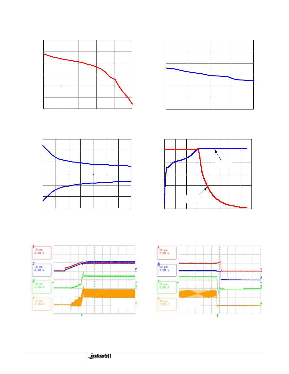
Typical Operating Performance DCIN = 20V, 3S2P Li-Battery, T
5.15
5.10
5.05
5.00
VDDP (V)
4.95
4.90
4.85
020406080100
VDDP LOAD CURRENT (mA)
FIGURE 3. VDD LOAD REGULATION
15
10
5
0
-5
ICM ACCURACY (%)
-10
3.23
3.22
3.21
3.20
VREF (V)
3.19
3.18
3.17
13.0
12.5
12.0
11.5
11.0
BATTERY VOLTAGE
10.5
= +25°C, unless otherwise noted.
A
0 50 100 150 200
I VREF (µA)
FIGURE 4. VREF LOAD REGULATION
VCHG (V)
ICHG (A)
1.0%
0.5%
0.0%
-0.5%
-1.0%
3.5
3.0
2.5
2.0
1.5
1.0
0.5
BATTERY CURRENT
-15
123 567
48
ADAPTER CURRENT (A)
FIGURE 5. ICM ACCURACY vs AC-ADAPTER CURRENT
VCOMP
ICOMP
CHARGE
CURRENT
INDUCTOR
CURRENT
FIGURE 7. CHARGE ENABLE
10.0
0 20406080100120140160
TIME (MINUTES)
0.0
FIGURE 6. TYPICAL CHARGING VOLTAGE AND CURRENT
ICOMP
VCOMP
CHARGE
CURRENT
INDUCTOR
CURRENT
FIGURE 8. CHARGE DISABLE
6
FN6738.1
January 7, 2009
ISL88731A
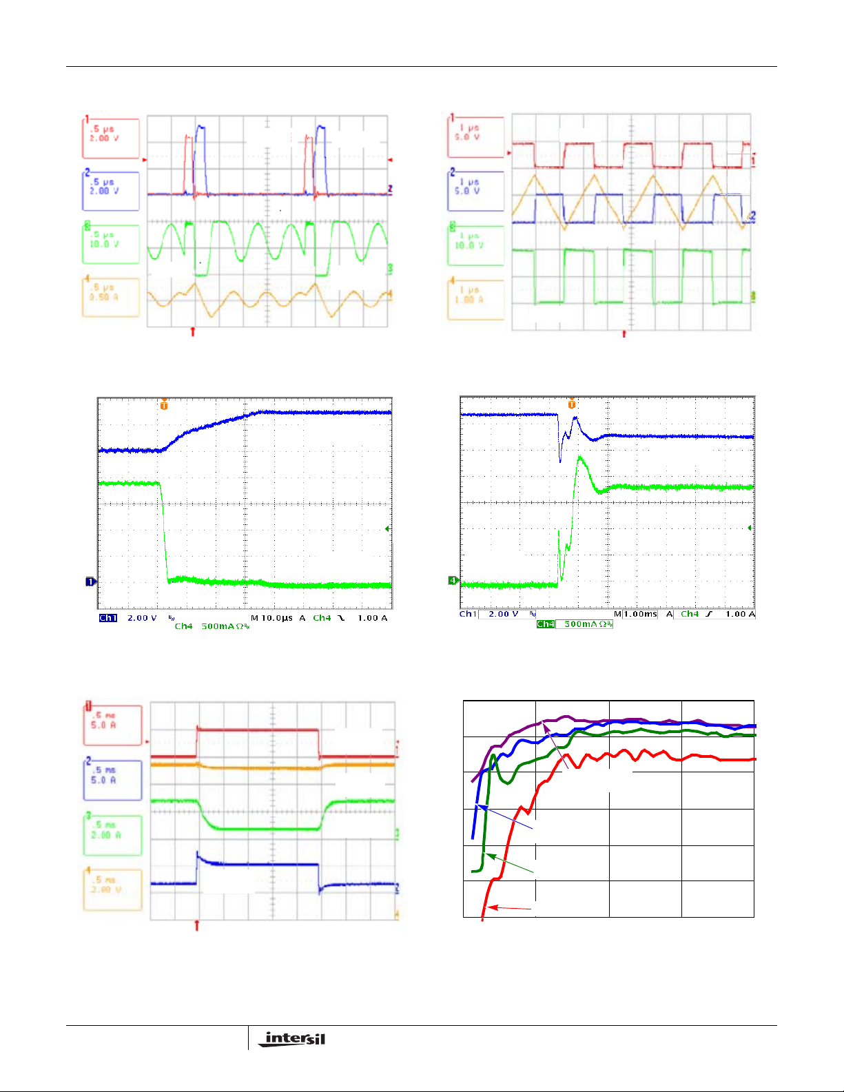
Typical Operating Performance DCIN = 20V, 3S2P Li-Battery, T
UGATE
PHASE
FIGURE 9. SWITCHING WAVEFORMS AT DIODE EMULATION
CSON/
V
BATTERY
LGATE
INDUCTOR
CURRENT
FIGURE 10. SWITCHING WAVEFORMS IN CC MODE
= +25°C, unless otherwise noted. (Continued)
A
UGATE
INDUCTOR
CURRENT
LGATE
PHASE
CSON/
V
BATTERY
BATTERY
CURRENT
FIGURE 11. BATTERY REMOVAL
SYSTEM
LOAD
BATTERY
VOLTAGE
CHARGE
CURRENT
ADAPTER
CURRENT
FIGURE 13. LOAD TRANSIENT RESPONSE
BATTERY
CURRENT
FIGURE 12. BATTERY INSERTION
100
95
90
85
80
75
70
04 8
16.8V
BATTERY
12.6V
BATTERY
8.4V
BATTERY
4.2V
BATTERY
26
CHARGE CURRENT (A)
FIGURE 14. EFFICIENCY vs CHARGE CURRENT AND
BATTERY VOLTAGE (EFFICIENCY DC
= 20V)
IN
7
FN6738.1
January 7, 2009
 Loading...