

®
www.BDTIC.com/Intersil
ISL88021, ISL88022
Data Sheet September 18, 2006
Triple Voltage Monitor with Adjustable
Power-On-Reset and Undervoltage/
Overvoltage Monitoring Capability
The ISL88021 and ISL88022 family of devices are
customizable triple voltage-monitoring supervisors that
assert a reset if any of the monitored voltages becomes
non-compliant. They offer popular functions such as
Power-On-Reset timing control with both RESET and
RESET
outputs, Supply Voltage Supervision, both under or
overvoltage detection, and Manual Reset assertion. By
offering these features i n a sma ll 8 Ld MS OP package, the
ISL88021 and ISL88022 can lower system cost, reduce
board space requirements and increase the reliability of
systems.
Applying a voltage to V
circuit which holds RESET
time. This allows the power supply and system oscillator to
stabilize before the processor can execute code.
Low V
detection circuitry protects the user’s system from
DD
low voltage conditions, resetting the system when V
below its minimum preset voltage threshold V
remains asserted until V
level and stabilizes. Two additional voltage monitoring
inputs, V2MON (preset) and V3MON (adjustable), monitor
other supplies to provide reliable system operation.
The ISL88021 V3MON input monitors for undervoltage (UV)
conditions whereas the ISL88022 V3MON input allows
monitoring for overvoltage (OV) conditions. The monitored
voltage on V3MON on either device is compared via a
resistor divider to a 600mV internal reference. Hence, any
voltage more or less positive than this reference can be
accurately monitored to meet specific system level
requirements or to fine-tune the threshold for applications
requiring higher precision.
These devices also let users increase the Power-On-Reset
time-out delay by connecting a capacitor between C
ground. This lengthens the period of an internal clock
counter thereby increasing the time between voltage
compliance and reset outputs signaling.
activates the Power-On-Reset
DD
low for an adjustable period of
returns to its proper operating
DD
TH1
DD
. Reset
POR
falls
and
FN8226.1
Features
• Triple Voltage Monitor and Reset Assertion
•Low V
Detection and Reset Assertion
DD
- Adjustable Reset Threshold Voltages
- 0.6V ±6mV Over -40°C to +85°C
- Reset Signal Valid to V
DD
= 1V
• 140ms Minimum Reset Pulse Delay that is Customizable
Using an External Capacitor
• Both RST and RST Outputs Available
• Undervoltage/Overvoltage Monitoring Capability
• Low 20µA Consumptio n
• Small 8 Ld MSOP Package
• Pb-Free Plus Anneal Available (RoHS Compliant)
Applications
• Process Control Systems
• Intelligent Instruments
• Embedded Control Systems
• Computer Systems
• Portable/Battery-Powered Equipment
• Multi-Voltage Systems
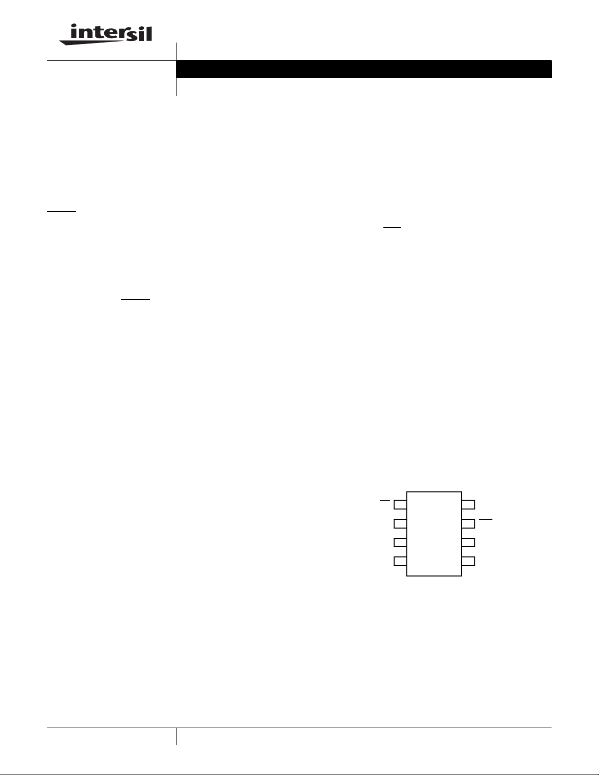
Pinout
ISL88021, ISL88022
(8 LD MSOP)
TOP VIEW
MR
V
DD
V2MON
GND
1
2
3
4
8
RST
7
RST
6
C
POR
5
V3MON
A manual reset input provides debounce circuitry for
minimum reset component count.
1
CAUTION: These devices are sensitive to electrostatic discharge; follow proper IC Handling Procedures.
1-888-INTERSIL or 1-888-468-3774
| Intersil (and design) is a registered trademark of Intersil Americas Inc.
All other trademarks mentioned are the property of their respective owners.
Copyright Intersil Americas Inc. 2006. All Rights Reserved
ISL88021, ISL88022
www.BDTIC.com/Intersil
Ordering Information (See Notes)
V2MO
V
TRIP2
V3MON
TYPE PACKAGE
PART
NUMBER
ISL88021IU8FAZ ANM 3.09V 1.69V UV 8 Ld MSOP
ISL88021IU8FCZ ANL 3.09V 2.32V UV 8 Ld MSOP
ISL88021IU8FEZ 3.09V 2.92V UV 8 Ld MSOP
ISL88021IU8FFZ 3.09V 3.09V UV 8 Ld MSOP
ISL88021IU8HAZ 4.64V 1.69V UV 8 Ld MSOP
ISL88021IU8HCZ 4.64V 2.32V UV 8 Ld MSOP
ISL88021IU8HEZ ANK 4.64V 2.92V UV 8 Ld MSOP
ISL88021IU8HFZ ANJ 4.64V 3.09V UV 8 Ld MSOP
ISL88022IU8FAZ ANQ 3.09V 1.69V OV 8 Ld MSOP
ISL88022IU8FCZ ANP 3.09V 2.32V OV 8 Ld MSOP
ISL88022IU8FEZ 3.09V 2.92V OV 8 Ld MSOP
ISL88022IU8FFZ 3.09V 3.09V OV 8 Ld MSOP
PART
MARKING
V
V
TRIP1
DD
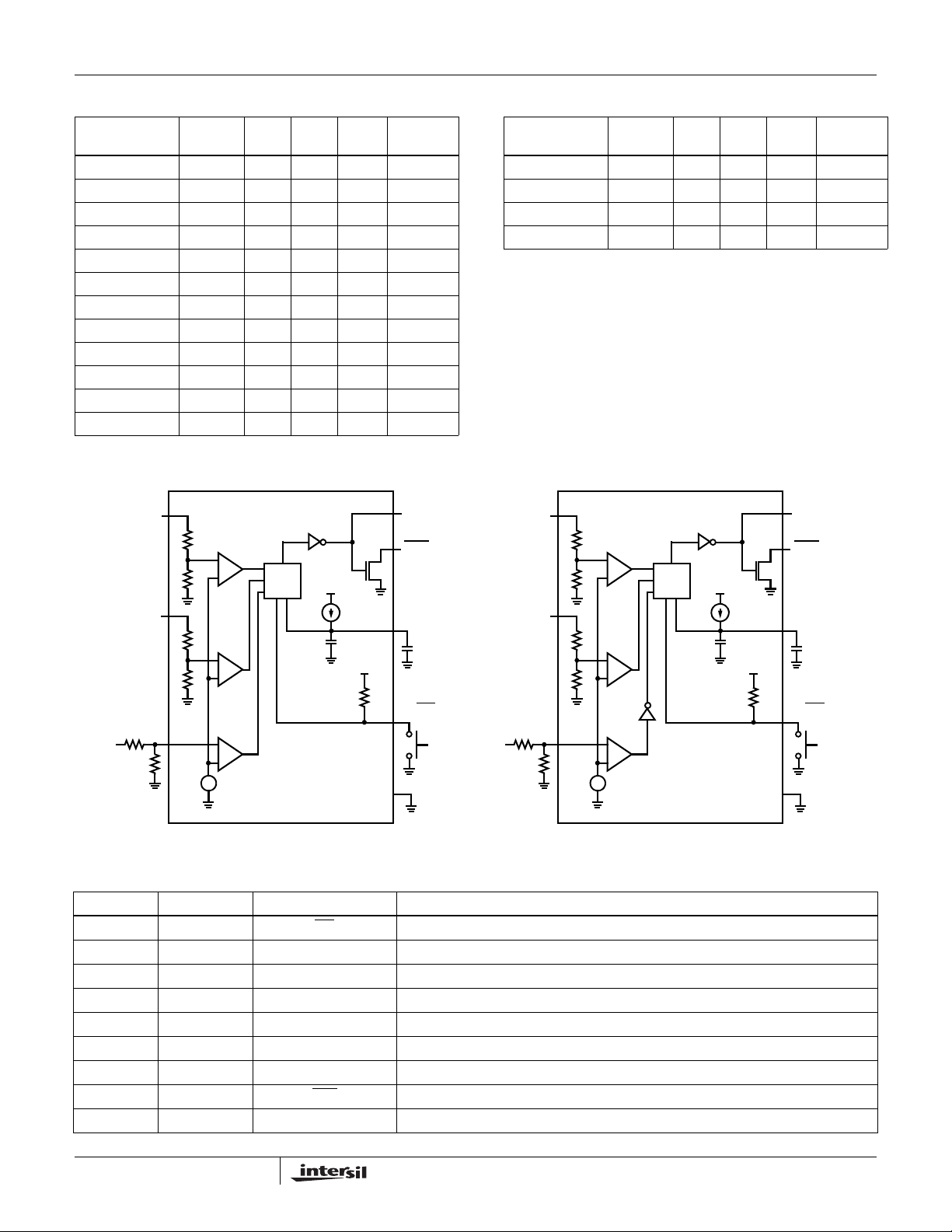
Block Diagrams
V
DD
RST
RST
Ordering Information (See Notes) (Continued)
V2MO
V
TRIP2
V3MON
TYPE PACKAGE
RST
RST
PART
NUMBER
ISL88022IU8HAZ 4.64V 1.69V OV 8 Ld MSOP
ISL88022IU8HCZ 4.64V 2.32V OV 8 Ld MSOP
ISL88022IU8HEZ ANO 4.64V 2.92V OV 8 Ld MSOP
ISL88022IU8HFZ ANN 4.64V 3.09V OV 8 Ld MSOP
NOTES:
1. Standard versions are shown in bold. For non-standard versions,
please contact factory for availability.
2. Add “-TK” suffix for Tape and Reel.
3. Intersil Pb-free plus anneal products employ special Pb-free
material sets; molding compounds/die attach materials and 100%
matte tin plate termination finish, which are RoHS compliant and
compatible with both SnPb and Pb-free soldering operations.
Intersil Pb-free products are MSL classified at Pb-free peak reflow
temperatures that meet or exceed the Pb-free requirements of
IPC/JEDEC J STD-020.
V
DD
PART
MARKING
V
V
TRIP1
DD
POR
V2MON
V3MON
C
POR
MR
PB
V
REF
±
ISL88021
GND
V2MON
V3MON
V
REF
±
Pin Descriptions
ISL88021 ISL88022 NAME FUNCTION
11 MR
22 V
3 3 V2MON Second Undervoltage Monitor Input
4 4 GND Ground
5 V3MON Undervoltage Monitor Input
5 V3MON Overvoltage Monitor Input
66 C
77 RST
8 8 RST Active-High Push-Pull Reset Output
DD
POR
Active-Low Open Drain Manual Reset Input
Power Supply Input
Set Power-On-Reset Timeout Delay
Active-Low Open Drain Reset Output
POR
ISL88022
GND
C
POR
MR
PB
2
FN8226.1
September 18, 2006
ISL88021, ISL88022
www.BDTIC.com/Intersil
Absolute Maximum Ratings Thermal Information
Temperature Under Bias . . . . . . . . . . . . . . . . . . . . -40C to +85C
Voltage on Any Pin with Respect to GND . . . . . . . . . . .-1.0V to +7V
D.C. Output Current. . . . . . . . . . . . . . . . . . . . . . . . . . . . . . . . . . 5mA
Recommended Operating Conditions
Industrial . . . . . . . . . . . . . . . . . . . . . . . . . . . . . . . . . .-40°C to +85°C
CAUTION: Stresses above those listed in “Absolute Maximum Ratings” may cause permanent damage to the device. This is a stress only rating and operation of the
device at these or any other conditions above those indicated in the operational sections of this specification is not implied.
NOTE:
is measured with the component mounted on a high effective thermal conductivity test board in free air. See Tech Brief TB379 for details.
1. θ
JA
Thermal Resistance (Typical, Note 1) θ
MSOP Package . . . . . . . . . . . . . . . . . . . . . . . . . . . . 145
Maximum Junction Temperature (Plastic Package) . . . . . . .+150°C
Maximum Storage Temperature Range. . . . . . . . . .-65°C to +150°C
Maximum Lead Temperature (Soldering 10s) . . . . . . . . . . . .+300°C
(MSOP - Lead Tips Only)
Electrical Specifications Over the recommended operating conditions unless otherwise specified.
SYMBOL PARAMETER TEST CONDITIONS MIN TYP MAX UNITS
V
DD
I
DD1
I
DD2
I
DDA
VOLTAGE THRESHOLDS
V
TH1
V
TH1HYST
V
TH2
V
TH2HYST
V
TH3
V
REFHYST
RESET
V
OL
V
OH
t
RPD
t
POR
C
LOAD
Supply Voltage Range 2.0 5.5 V
V
Supply Current V
DD
V2MON Input Current V2MON = 3.3V 5.5 6 µA
V3MON Input Current V3MON = 1.0V 19 100 nA
Fixed Voltage Trip Point for V
Hysteresis of V
Fixed Voltage Trip Point for V2MON ISL88021/22IU8xFZ 3.034 3.090 3.146 V
Hysteresis of V
V3MON Threshold Voltage VTH for V3MON on ISL88021 0.594 0.605 0.616 V
Hysteresis Voltage 3mV
Reset Output Voltage Low VDD ≥ 3.3V, Sinking 2.5mA 0.05 0.40 V
RST Output Voltage High VDD ≥ 3.3V, Sourcing 2.5mA VDD-0.6 VDD-0.4 V
VTH to Reset Asserted Delay 10 µs
POR Timeout Delay C
Load Capacitance on Reset Pins 5 pF
TH1
TH2
DD
= 5.0V 12.5 15 µA
DD
ISL88021/22IU8HxZ 4.565 4.649 4.733 V
ISL88021/22IU8FxZ 3.029 3.085 3.141 V
V
= 4.64V 46 mV
TH1
V
= 3.09V 37 mV
TH1
ISL88021/22IU8xEZ 2.894 2.947 3.000 V
ISL88021/22IU8xCZ 2.290 2.332 2.374 V
ISL88021/22IU8xAZ 1.660 1.690 1.720 V
V
= 3.09V 37 mV
TH2
V
= 2.92V 29 mV
TH2
V
= 2.32V 23 mV
TH2
= 2.19V 22 mV
V
TH2
V
= 1.69V 17 mV
TH2
for V3MON on ISL88022 0.587 0.595 0.603 V
V
TH
V
< 3.3V, Sinking 1.5mA 0.05 0.40 V
DD
< 3.3V, Sourcing 1.5mA VDD-0.6 VDD-0.4 V
V
DD
is open 140 200 ms
POR
JA
(°C/W)
3
FN8226.1
September 18, 2006

ISL88021, ISL88022
www.BDTIC.com/Intersil
Electrical Specifications Over the recommended operating conditions unless otherwise specified. (Continued)
SYMBOL PARAMETER TEST CONDITIONS MIN TYP MAX UNITS
MANUAL RESET
V
V
MRH
t
R
MRL
MR
PU
MR Input Voltage Low 0.8 V
MR Input Voltage High VDD-0.6 V
MR Minimum Pulse Width 550 ns
Internal Pull-Up Resistor 20 kΩ
Functional Description
The ISL88021 and ISL88022 devices incorporate such features
as Power-On-Reset control, Supply Voltage Supervision,
Undervoltage or Overvoltage Monitoring, and Manual Reset
Assertion.
The ISL88021 and ISL88022 devices provide common preset
threshold voltages on both V
optional resistor divider network on V3MON to provide custom
voltage monitoring of voltages greater than 0.6V. An optional
capacitor can be connected between the C
increase the nominal 200ms t
operational functionality with a timing diagram.
Voltage Monitoring
During normal operation, the ISL88021 and ISL88022 monitor
the voltage levels on V
ISL88021 asserts reset if any one of these voltages fall below
their respective voltage trip points and in the case of ISL88022
above the voltage trip point on the V3MON input. The reset
signal effectively prevents the microprocessor from operating
during a power failure, brownout or over voltage condition. This
signal remains active until all monitored voltages meet all
voltage threshold requirements for the reset time delay period
t
. Note that both RESET and RESET signals are provided
POR
for design flexibility. Figure 1 illustrates the VDD, V2MON and
V3MON input threshold voltages for the various available
options.
5.000
4.500
4.000
3.500
3.000
2.500
2.000
1.500
1.000
VDD, V2MON, V3MON Vth (V)
0.500
0.000
FIGURE 1. VDD, V2MON, V3MON VTH vs TEMP
DD
-40 25 85
and V2MON and for an
DD
pin and GND to
delay. Figure 7 illustrates
POR
POR
, V2MON and V3MON. The
Vth = 4.64V
Vth = 3.09V
Vth = 2.92V
Vth = 2.32V
Vth = 1.69V
Vth = 0.60V
TEMPERATURE (°C)
Power-On-Reset (POR)
Applying power to the ISL88021 and ISL88022 devices
activates a POR circuit which holds the RESET
V
> 1V. This signal provides several benefits:
DD
• It prevents the system microprocessor from starting to
operate with insufficient voltage.
• It prevents the processor from operating prior to
stabilization of the oscillator.
• It ensures that the monitored device is held out of operation
until internal registers are properly loaded.
• It allows time for an FPGA to download its configuration prior
to initialization of the circuit.
When all of the monitored voltages meet their respective
input voltage requirements for the specified reset timeout
delay t
output low and releases the RST
, the POR circuit simultaneously pulls the RST
POR
output to allow the system
to begin operation.
Adjusting t
POR
On the ISL88021 and ISL88022, users can adjust the
Power-On-Reset timeout delay (t
nominal t
on the C
. Figure 2 illustrates the effect of capacitance
POR
pin to ground, showing changing t
POR
) to many times the
POR
graph normalized to 175ms for an open C
maximum recommended capacitance that should be placed
on the C
pin is 50pF. NOTE: Care should be taken in
POR
PCB layout and capacitor placement in order to eliminate
stray capacitance as much as possible, which contributes to
t
error.
POR
10
8
POR
6
4
2
Normalized t
0
1 5 9 13 17 21 25 29 33 37 41 45
C
(pF)
POR
pin low once
POR
pin. The
POR
with a
FIGURE 2. NORMALIZED t
4
POR
vs C
GRAPH
POR
September 18, 2006
FN8226.1

ISL88021, ISL88022
www.BDTIC.com/Intersil
Manual Reset
The manual reset input (MR) allows the user to trigger a reset
by using a push-button switch or by signaling that pin low. The
MR
input is an active low debounced input. By connecting a
push-button directly from MR
manual system reset capability. Reset is asserted if the MR
is pulled low to less than 100mV for 1µs or longer while the
push-button is closed or a reset is signaled. After MR
released, the reset outputs remain asserted for t
has an internal 20kΩ
pull up resistor provided.
Figure 3 illustrates a typical application diagram for either IC
showing both reset outputs being used along with both a
manual and signalled reset configuration. The V
V2MON thresholds are preset whereas the V3MON is capable
of UV (ISL88021) or OV (ISL88022) monitoring of a voltage
greater than or less than 0.6V , respectively.
3.3V - 5V
1.8V - 3.3V
to ground, the designer adds
V
DD
V2MON
ISL88021
ISL88022
RST
RST
MR
is
. MR input
POR
and
DD
TO DISPLAY
TO µP
PB
pin
RESET
SIGNAL
ISL88021IU8HFZ
ISL88022IU8HFZ
C
V
> 0.6V
MON
FIGURE 3. TYPICAL APPLICATION DIAGRAM
V3MON
POR
GND
Application Considerations
Follow good decoupling practices to prevent transients from
causing unwanted reset signaling due to switching noises
and short duration droops.
When using the C
on this pin to minimize effect on t
C
pad is patterned, the t
POR
pin, reduce layout stray capacitance
POR
POR
timing. If no PCB
POR
can be 160ms.
Using the ISL88021_22EVAL1 Platform
The ISL88021_22EVAL1 board is designed to provide both
immediate functional assessment and flexibility to the user.
Both ICs are the ‘HF’ variant having a V
V2MON Vth of 3.09V and V3MON Vth of 0.6V. The top IC
position is the ISL88021 and is configured to monitor for
undervoltage (UV) compliance of a 5V, 3.3V and a 2.5V and
signaling the RESET and RESET
outputs. The bottom
position is the ISL88022 variant, which is configured to
measure a 3.3V overvoltage (OV) in addition to UV on both
the 5V and 3.3V supplies. RESET and RESET
at least t
when these voltage go out of range. In both
POR
cases V3MON interfaces with the monitored supply via a
simple resistor divider for comparison to the internal 0.6V
reference. A Manual Reset (MR
) input is provided on both
ICs and is invoked by pulling this input LOW.
Vth of 4.64V, a
DD
is asserted for
FIGURE 4. ISL88021_22EVAL1 SCHEMATIC AND PHOTO
MONITORED VOL TAGE RISING AND FALLING RAMP
THROUGH THE PROGRAMMED UV AND OV THRESHOLDS
RESET# RESPONDING TO
MONITORED VOLTAGE. C
PIN IS OPEN, t
FIGURE 5. ISL88022EVAL1 3.3V UV AND OV DETECTION
POR
= 150ms
POR
5
FN8226.1
September 18, 2006

3.3V RISING EDGE 100ms/DIV
www.BDTIC.com/Intersil
ISL88021, ISL88022
ISL88022 t
C
POR
FIGURE 6. ISL88021_22EVAL1 t
POR
= OPEN
= 150ms
ISL88021 t
C
POR
POR
= 10pF
Operational Timing Diagrams
V
TH1
V
DD
1V
V2MON or V3MON
(ISL88021)
= 390ms
POR
COMPARISON
V
or V
TH2
REF
>t
MR
MR
RST
RST
t
POR
t
RPD
t
POR
FIGURE 7. ISL88021 AND ISL88022 TIMING DIAGRAM
t
RPD
t
POR
t
POR
<t
MD
6
FN8226.1
September 18, 2006

ISL88021, ISL88022
www.BDTIC.com/Intersil
Mini Small Outline Plastic Packages (MSOP)
N
EE1
INDEX
AREA
AA1A2
-H-
SIDE VIEW
12
TOP VIEW
b
e
D
NOTES:
1. These package dimensions are within allowable dimensions of
JEDEC MO-187BA.
2. Dimensioning and tolerancing per ANSI Y14.5M-1994.
3. Dimension “D” does not include mold flash, protrusions or gate
burrs and are measured at Datum Plane. Mold flash, protrusion
and gate burrs shall not exceed 0.15mm (0.006 inch) per side.
4. Dimension “E1” does not include interlead flash or protrusions
and are measured at Datum Plane. Interlead flash and
protrusions shall not exceed 0.15mm (0.006 inch) per side.
5. Formed leads shall be planar with respect to one another within
0.10mm (0.004) at seating Plane.
6. “L” is the length of terminal for soldering to a substrate.
7. “N” is the number of terminal positions.
8. Terminal numbers are shown for reference only.
9. Dimension “b” does not include dambar protrusion. Allowable
dambar protrusion shall be 0.08mm (0.003 inch) total in excess
of “b” dimension at maximum material condition. Minimum space
between protrusion and adjacent lead is 0.07mm (0.0027 inch).
- H -
-A -
.
10. Datums and to be determined at Datum plane
11. Controlling dimension: MILLIMETER. Converted inch dimensions are for reference only.
-B-
0.20 (0.008) A
GAUGE
PLANE
SEATING
PLANE
0.10 (0.004) C
-A-
0.20 (0.008) C
- B -
0.25
(0.010)
-C-
SEATING
PLANE
a
0.20 (0.008) C
- H -
B
4X θ
C
D
4X θ
L1
C
L
E
1
END VIEW
R1
R
L
C
-B-
M8.118 (JEDEC MO-187AA)
8 LEAD MINI SMALL OUTLINE PLASTIC PACKAGE
INCHES MILLIMETERS
SYMBOL
A 0.037 0.043 0.94 1.10 -
A1 0.002 0.006 0.05 0.15 -
A2 0.030 0.037 0.75 0.95 -
b 0.010 0.014 0.25 0.36 9
c 0.004 0.008 0.09 0.20 -
D 0.116 0.120 2.95 3.05 3
E1 0.116 0.120 2.95 3.05 4
e 0.026 BSC 0.65 BSC -
E 0.187 0.199 4.75 5.05 -
L 0.016 0.028 0.40 0.70 6
L1 0.037 REF 0.95 REF -
N8 87
R 0.003 - 0.07 - -
R1 0.003 - 0.07 - -
05
α
o
o
0
15
o
o
6
o
5
o
0
15
o
o
6
Rev. 2 01/03
NOTESMIN MAX MIN MAX
-
-
All Intersil U.S. products are manufactured, assembled and tested utilizing ISO9000 quality systems.
Intersil Corporation’s quality certifications can be viewed at www.intersil.com/design/quality
Intersil products are sold by description only. Intersil Corporation reserves the right to make changes in circuit design, software and/or specifications at any time without
notice. Accordingly, the reader is cautioned to verify that data sheets are current before placing orders. Information furnished by Intersil is believed to be accurate and
reliable. However, no responsibility is assumed by Intersil or its subsidiaries for its use; nor for any infringements of patents or other rights of third parties which may result
from its use. No license is granted by implic atio n or other wise u nde r any p a tent or patent rights of Intersil or i t s sub sidi aries.
For information regarding Intersil Corporation and its products, see www.intersil.com
7
FN8226.1
September 18, 2006
 Loading...