


®
ISL88011, ISL88012, ISL88013,
ISL88014, ISL88015
Data Sheet December 14, 2006
5 Ld Voltage Supervisors with Adjustable
Power-On Reset, Dual Voltage Monitoring
or Watchdog Timer Capability
The ISL88011 through ISL88015 family of devices offer both
fixed and/or adjustable voltage-monitoring that combine
popular functions such as Power On Reset control,
Watchdog Timer, Supply Voltage Supervision, and Manual
Reset assertion in a small 5 Ld SOT-23 package.
Unique features on the ISL88013 and ISL88015 include a
watchdog timer with a 51s startup timeout and a 1.6s normal
timeout duration. On the ISL88011 and ISL88014, users can
increase the nominal 200ms Power On Reset timeout delay
by adding an external capacitor to the C
and adjustable voltage monitors are provided by the
ISL88012. Complementary active-low and active-high reset
outputs are available on the ISL88011, ISL88012 and
ISL88013 devices. All devices provide manual reset
capability (see “Product Features Table” on page 4).
Seven preprogrammed reset threshold voltages accurate to
±1.5% over temperature are offered (see “Ordering
Information” on page 3). The ISL88012, ISL88014 and
ISL88015 have a user-adjustable voltage input available for
custom monitoring of any voltage down to 0.6V. All p art s are
specifically designed for low power consumption and high
threshold accuracy.
pin. Both fixed
POR
FN8093.1
Features
• Single/Dual Voltage Monitoring Supervisors
• Fixed-Voltage Options Allow Precise Monitoring of +2.5V,
+3.0V, +3.3V, and +5.0V Power Supplies
• Dual Supervisor Has One Fixed Voltage Input and Another
That is User-Adjustable Down to 0.6V.
• Both RST and RST
• Adjustable POR Timeout Delay Options
• Watchdog Timer With 1.6s Normal and 51s Startup
Timeout Durations
• Manual Reset Input on All Devices
• Reset Signal Valid Down to VDD = 1V
• Accurate ±1.5% Voltage Threshold
• Immune to Power-Supply Transients
• Ultra Low 5.5µA Supply Current
• Small 5 Ld SOT-23 Pb-Free Package
• Pb-Free Plus Anneal Available (RoHS Compliant)
Outputs Available
Applications
• Process Control Systems
• Intelligent Instruments
• Embedded Control Systems
• Computer Systems
• Critical µP and µC Power Monitoring
• Portable/Battery-Powered Equipment
• PDA and Handheld PC Devices
1
CAUTION: These devices are sensitive to electrostatic discharge; follow proper IC Handling Procedures.
1-888-INTERSIL or 1-888-468-3774
| Intersil (and design) is a registered trademark of Intersil Americas Inc.
All other trademarks mentioned are the property of their respective owners.
Copyright Intersil Americas Inc. 2006. All Rights Reserved
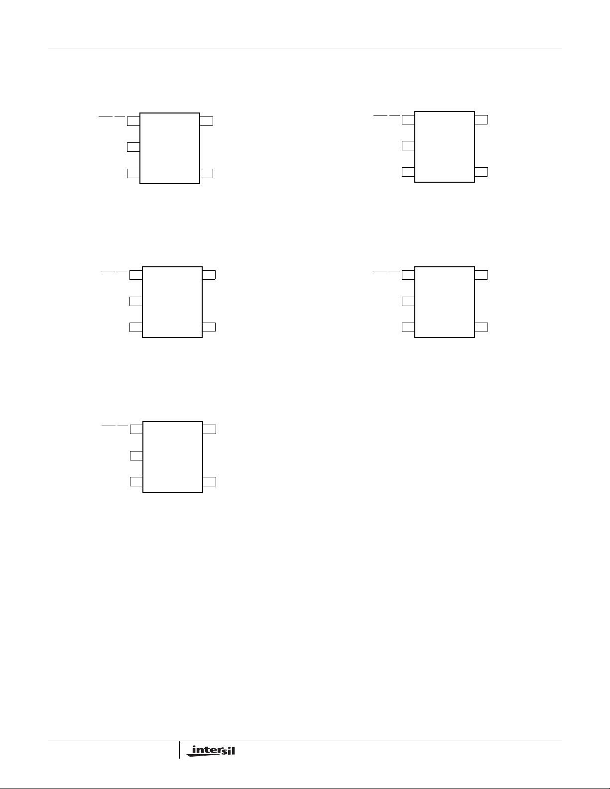
Pinouts
ISL88011, ISL88012, ISL88013, ISL88014, ISL88015
ISL88011
(5 LD SOT-23)
TOP VIEW
ISL88012
(5 LD SOT-23)
TOP VIEW
RST/MR
GND
RST
RST/MR
GND
RST
1
2
3
ISL88013
(5 LD SOT-23)
TOP VIEW
1
2
3
ISL88015
(5 LD SOT-23)
TOP VIEW
5
VDD
CPOR
4
RST/MR
GND
RST
1
2
3
5
VDD
VMON
4
ISL88014
(5 LD SOT-23)
TOP VIEW
5
VDD
WDI
4
RST/MR
GND
VMON
1
2
3
5
VDD
CPOR
4
RST/MR
GND
VMON
5
1
2
3
VDD
WDI
4
2
FN8093.1
December 14, 2006
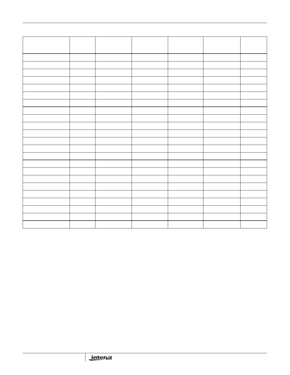
Ordering Information
ISL88011, ISL88012, ISL88013, ISL88014, ISL88015
TEMPERATURE
PART NUMBER
(Notes 1, 2)
ISL88011IH546Z-TK AGU 4.64 N/A -40 to +85 5 Ld SOT-23 P5.064
ISL88011IH544Z-TK AGV 4.38 N/A -40 to +85 5 Ld SOT-23 P5.064
ISL88011IH531Z-TK AGW 3.09 N/A -40 to +85 5 Ld SOT-23 P5.064
ISL88011IH529Z-TK AGX 2.92 N/A -40 to +85 5 Ld SOT-23 P5.064
ISL88011IH526Z-TK AGY 2.63 N/A -40 to +85 5 Ld SOT-23 P5.064
ISL88011IH523Z-TK AGZ 2.32 N/A -40 to +85 5 Ld SOT-23) P5.064
ISL88011IH522Z-TK AHE 2.19 N/A -40 to +85 5 Ld SOT-23 P5.064
ISL88012IH546Z-TK AHF 4.64 0.6 (Note 2) -40 to +85 5 Ld SOT-23 P5.064
ISL88012IH544Z-TK AHG 4.38 0.6 (Note 2) -40 to +85 5 Ld SOT-23 P5.064
ISL88012IH531Z-TK AHH 3.09 0.6 (Note 2) -40 to +85 5 Ld SOT-23 P5.064
ISL88012IH529Z-TK AHI 2.92 0.6 (Note 2) -40 to +85 5 Ld SOT-23 P5.064
ISL88012IH526Z-TK AHJ 2.63 0.6 (Note 2) -40 to +85 5 Ld SOT-23 P5.064
ISL88012IH523Z-TK AHK 2.32 0.6 (Note 2) -40 to +85 5 Ld SOT-23 P5.064
ISL88012IH522Z-TK AHL 2.19 0.6 (Note 2) -40 to +85 5 Ld SOT-23 P5.064
ISL88013IH546Z-TK AHM 4.64 N/A -40 to +85 5 Ld SOT-23 P5.064
ISL88013IH544Z-TK AHN 4.38 N/A -40 to +85 5 Ld SOT-23 P5.064
ISL88013IH531Z-TK AHO 3.09 N/A -40 to +85 5 Ld SOT-23 P5.064
ISL88013IH529Z-TK AHP 2.92 N/A -40 to +85 5 Ld SOT-23 P5.064
ISL88013IH526Z-TK AHQ 2.63 N/A -40 to +85 5 Ld SOT-23 P5.064
ISL88013IH523Z-TK AHR 2.32 N/A -40 to +85 5 Ld SOT-23 P5.064
ISL88013IH522Z-TK AHS 2.19 N/A -40 to +85 5 Ld SOT-23 P5.064
ISL88014IH5Z-TK AHT N/A 0.6 (Note 2) -40 to +85 5 Ld SOT-23 P5.064
ISL88015IH5Z-TK AHU N/A 0.6 (Note 2) -40 to +85 5 Ld SOT-23 P5.064
NOTES:
1. Intersil Pb-free plus anneal products employ special Pb-free material sets; molding compounds/die attach materials and 100%
matte tin plate termination finish, which are RoHS compliant and compatible with both SnPb and Pb-free soldering operations.
Intersil Pb-free products are MSL classified at Pb-free peak reflow temperatures that meet or exceed the Pb-free requirements
of IPC/JEDEC J STD-020
2. The voltage trip point can be adjusted to be greater than 0.6V using 2 external resistors. By default, the VTHVMON trip point is
0.6V if no external resistors are used.
PART
MARKING
V
THVDD
(V)
V
THVMON
(V)
RANGE
(°C)
PACKAGE
TAPE AND REEL
(Pb-free)
DWG. #
PKG.
3
FN8093.1
December 14, 2006
ISL88011, ISL88012, ISL88013, ISL88014, ISL88015
Functional Block Diagrams
V
DD
POR
±
C
POR
V
THMON
OSC
V
DD
GND
ISL88011
V
DD
R
1
VMON
R
2
±
V
THMON
C
POR
RST/MR
PB
RST
POR
V
DD
OSC
ISL88014
V
VMON
RST/MR
RST
THMON
V
DD
PB
WDI
POR
±
V
THMON
OSC
WDT
RST/MR
PB
RST
GND
ISL88013
POR
OSC
WDT
RST/MR
PB
GND
DD
POR
±
V
THMON
±
V
REF
GND
ISL88012
V
DD
R
RST/MR
GND
1
VMON
R
PB
2
±
V
WDI
ISL88015
Product Features Table
FUNCTION ISL88011 ISL88012 ISL88013 ISL88014 ISL88015
Active-Low Reset (RST) xxxxx
Active-High Reset (RST) xxx
Watchdog Timer (WDI) xx
Dual Voltage Supervision x
Adjustable POR Timeout (C
Manual Reset Input (MR
Fixed Trip Point Voltage xxx
Adjustable Trip Point Voltage xxx
) xx
POR
) xxxxx
Pin Descriptions
PIN
NAME FUNCTIONISL88011 ISL88012 ISL88013 ISL88014 ISL88015
11111RST
22222GND Ground
433VMON Adjustable Threshold Voltage Input
333 RST Active-High Reset Output
44C
44WDI Watchdog Timer Input
55555V
4
/MR Combined Active-Low Reset Output and Manual Reset Input
POR
DD
Adjustable POR Timeout Delay Input
Supply Voltage and Monitored Input
FN8093.1
December 14, 2006

ISL88011, ISL88012, ISL88013, ISL88014, ISL88015
Absolute Maximum Ratings Recommended Operating Conditions
Temperature under bias. . . . . . . . . . . . . . . . . . . . . .-40°C to +125°C
Storage temperature . . . . . . . . . . . . . . . . . . . . . . . .-65°C to +150°C
Voltage on any pin with respect to GND . . . . . . . . . . . .-1.0V to +7V
D.C. output current. . . . . . . . . . . . . . . . . . . . . . . . . . . . . . . . . . . 5mA
Lead temperature (soldering, 10 seconds) . . . . . . . . . . . . . .+300°C
Recommended Operating Conditions
Temperature Range (Industrial) . . . . . . . . . . . . . . . . .-40°C to +85°C
Pull-up Resistance (R
CAUTION: Absolute Maximum Ratings indicate limits beyond which permanent damage to the device and impaired reliability may occur. These are stress ratings
provided for information only and functional operation of the device at these or any other conditions beyond those indicated in the operational sections of this
specification are not implied.
For guaranteed specifications and test conditions, see Electrical Specifications. The guaranteed specifications apply only for the test conditions listed. Some
performance characteristics may degrade when the device is not operated under the listed test conditions.
NOTE:
is measured with the component mounted on a high effective thermal conductivity test board in free air. See Tech Brief TB379 for details.
3. θ
JA
) . . . . . . . . . . . . . . . . . . . . . 5kΩ to 100kΩ
PU
Thermal Resistance (Typical, Note 3) θJA (°C/W)
5 Ld SOT-23. . . . . . . . . . . . . . . . . . . . . . . . . . . . . . . 190
Maximum Junction Temperature (Plastic Package) . . . . . . . +125°C
Maximum Storage Temperature Range. . . . . . . . . .-65°C to +150°C
Maximum Lead Temperature (Soldering 10s) . . . . . . . . . . . . +300°C
(SOT-23 Lead Tips Only)
Electrical Specifications Over the recommended operating conditions unless otherwise specified, R
= 10kΩ.
PU
SYMBOL PARAMETER TEST CONDITIONS MIN TYP MAX UNITS
V
DD
I
DD
I
LI
I
LO
Supply Voltage Range 2.0 5.5 V
Supply Current for ISL88011,
ISL88012, ISL88013
Supply Current for ISL88014,
ISL88015
VDD = 5.0V 8 11.5 µA
= 3.3V 7 10 µA
V
DD
= 2.5V 5.5 9 µA
V
DD
= 3.3V 4.5 8 µA
V
DD
Input Leakage Current (VMON) 100 nA
Output Leakage Current (VMON) 100 nA
VOLTAGE THRESHOLDS
V
THVDD
Fixed VDD Voltage Trip Point ISL88011, 88012, 88013IH546 4.57 4.64 4.71 V
ISL88011, 88012, 88013IH544 4.31 4.38 4.45 V
ISL88011, 88012, 88013IH531 3.04 3.09 3.14 V
ISL88011, 88012, 88013IH529 2.88 2.92 2.96 V
ISL88011, 88012, 88013IH526 2.59 2.63 2.67 V
ISL88011, 88012, 88013IH523 2.29 2.32 2.35 V
ISL88011, 88012, 88013IH522 2.16 2.19 2.22 V
V
THVDD
HYST
V
THVMON
V
THVMON
Hysteresis at VDD Input V
V
V
V
V
V
V
Adj. Reset Voltage Trip Point (Note 4) V
V
V
V
V
V
V
Adj. Reset Voltage Trip Point (Note 5) 594 600 606 mV
= 4.64V 46 mV
THVDD
= 4.38V 44 mV
THVDD
= 3.09V 31 mV
THVDD
= 2.92V 29 mV
THVDD
= 2.63V 26 mV
THVDD
= 2.32V 23 mV
THVDD
= 2.19V 22 mV
THVDD
= 4.64V 599 605 611 mV
THVDD
= 4.38V 597 603 609 mV
THVDD
= 3.09V 589 595 601 mV
THVDD
= 2.92V 589 595 601 mV
THVDD
= 2.63V 589 595 601 mV
THVDD
= 2.32V 597 603 609 mV
THVDD
= 2.19V 597 603 609 mV
THVDD
5
FN8093.1
December 14, 2006

ISL88011, ISL88012, ISL88013, ISL88014, ISL88015
Electrical Specifications Over the recommended operating conditions unless otherwise specified, R
SYMBOL PARAMETER TEST CONDITIONS MIN TYP MAX UNITS
V
THVMON
HYST
RESET
V
OL
V
OH
t
RPD
t
POR
C
LOAD
MANUAL RESET
V
MR
t
MR
WATCHDOG TIMER (Note 6)
Start t
t
WDT
t
WDPS
V
IL
V
IH
I
WDT
NOTES:
4. Applies to ISL88012
5. Applies to ISL88014 and ISL88015.
6. Applies to ISL88013 and ISL88015.
Hysteresis Voltage (Notes 4, 5) 3 mV
Reset Output Voltage Low VDD ≥ 3.3V, Sinking 0.5mA 0.05 0.40 V
V
< 3.3V, Sinking 0.5mA 0.05 0.40 V
DD
Reset Output Voltage High VDD ≥ 3.3V, Sourcing 0.4mA VDD-0.6 VDD-0.4 V
< 3.3V, Sourcing 0.4mA VDD-0.6 VDD-0.4 V
V
DD
VTH to Reset Asserted Delay 60 µs
POR Timeout Delay ISL88012, ISL88013, ISL88015 140 200 260 ms
ISL88011, ISL88014 with C
Load Capacitance on Reset Pins 5 pF
MR Input Voltage 0 100 mV
MR Minimum Pulse Width 1 µs
Startup Watchdog Timeout Period 32 51 64 sec
WDT
Normal Watchdog Timeout Period 1.0 1.6 2.0 sec
WDI Minimum Pulse Width 100 ns
Watchdog Input Voltage Low 0.3 x V
Watchdog Input Voltage High 0.85 x V
Watchdog Input Current 100 nA
= OPEN 200 250 ms
POR
DD
= 10kΩ. (Continued)
PU
DD
V
V
Pin Description
RST
The push-pull RST output is set to VDD (HIGH) whenever 1)
the device is first powered up, 2) either V
VMON falls below their respective minimum voltage sense
levels, 3) MR
is asserted or 4) the watchdog timeout expires.
RST/MR
This pin functions as both a reset output and a manual reset
input. The RST
complementary RST output but is an open drain output that
is pulled to GND (LOW) when reset is asserted. The MR
input is an active-low debounced input to which a user can
connect a push-button to add manual reset capability or
drive with active low signal from a controller.
V
DD
The V
DD
the ISL88011, ISL88012 and ISL88013. For these devices,
the voltage at this pin is compared against an internal
factory-programmed voltage trip point, V
first asserted when the device is initially powered up to
ensure that the power supply has stabilized. Thereafter,
reset is again asserted whenever V
output functions identically to the
pin is the power supply terminal. It is monitored by
or the voltage on
DD
THVDD
falls below V
DD
. A reset is
THVDD
The device is designed with hysteresis to help prevent
chattering due to noise.
VMON
The VMON pin on the ISL88012, ISL88014 and ISL88015 is
a monitored input voltage that is user-adjustable. The
voltage at this pin is compared against an internal 600mV
reference voltage (V
THVMON
) and a reset is asserted
whenever the monitored voltage falls below this trip point.
WDI
The Watchdog Input takes an input from a microprocessor
and ensures that it periodically toggles the WDI pin,
otherwise the internal watchdog timer runs out and reset is
asserted. The internal Watchdog Timer is cleared whenever
the WDI input pin sees a rising or falling edge or the device
is manually reset.
C
POR
The C
timeout delay (t
C
POR
.
input pin lets users increase the Power On Reset
POR
) by connecting a capacitor between
POR
and ground. (See Figure 3)
6
FN8093.1
December 14, 2006

V
DD
VMON
MR
RST
RST
V
THVDD
1V
ISL88011, ISL88012, ISL88013, ISL88014, ISL88015
V
THVMON
t
POR
t
RPD
t
POR
t
RPD
t
POR
>t
MR
t
POR
FIGURE 1. VOLTAGE MONITORING TIMING DIAGRAM
Principles of Operation
The ISL88011 through ISL88015 devices provide those
functions needed for critical voltage monitoring. These
features include Power On Reset control, customizable
supply voltage supervision, Watchdog Timer capability, and
manual reset assertion. By integrating all of these features
into a small 5 Ld SOT-23 package and using only 5.5µA of
supply current, the ISL88011 through ISL88015 devices can
assist in lowering system cost, reducing board space
requirements, and increasing the reliability of a system.
Low Voltage Monitoring
During normal operation, these supervisors monitor both the
voltage level of V
VMON (ISL88012, ISL88014, ISL88015). The device asserts
a reset if any of these voltages falls below their respective
trip points. The reset signal effectively prevents the system
from operating during a power failure or brownout condition.
This reset signal remains asserted until V
on VMON exceed their voltage threshold setting for the reset
time delay period t
(ISL88011, ISL88012, ISL88013) and/or
DD
and the voltage
DD
of 200ms (See Figure 1).
POR
The ISL88012, ISL88014 and ISL88015 allow users to
customize the minimum voltage sense level on the VMON
input pin. To do this, connect an external resistor divider
network to the VMON pin in order to set the trip point to
some voltage above 600mV according to the following
equation (See Figure 2):
R1R2+()
IN
0.6
-------------------------- -
×=
R
VMON
R
1
R
2
ISL88012
ISL88014
2
ISL88015
V
INTRIP
V
FIGURE 2. USING VMON TO MONITOR VIN VIA RESISTORS
(EQ. 1)
7
FN8093.1
December 14, 2006

ISL88011, ISL88012, ISL88013, ISL88014, ISL88015
Power On Reset (POR)
Applying at least 1V to the VDD pin activates a POR circuit
which asserts reset (i.e. RST goes HIGH while RST
LOW). The reset signals remain asserted until the voltage at
V
and/or VMON rise above the minimum voltage sense
DD
level for time period t
. This ensures that the voltages
POR
have stabilized.
These reset signals provide several benefits:
• It prevents the system microprocessor from starting to
operate with insufficient voltage.
• It prevents the processor from operating prior to
stabilization of the oscil l a to r.
• It ensures that the monitored device is held out of
operation until internal registers are properly loaded.
• It allows time for an FPGA to download its configuration
prior to initialization of the circuit.
Adjusting POR Timeout via C
POR
Pin
On the ISL88011 and ISL88014, users can adjust the Power
On Reset timeout delay (t
t
of 250ms. To do this, connect a capacitor between
POR
C
and ground (see Figure 3). For example, connecting a
POR
30pF capacitor to C
POR
) up to many times the normal
POR
will increase t
from a typical
POR
250ms to about 2.5s. NOTE: Care should be taken in PCB
layout and capacitor placement in order to reduce stray
capacitance as much as possible, which lengthens the t
timeout period.
goes
POR
Manual Reset
The manual reset input (MR) allows the user to trigger a
reset by using a push-button switch. The MR
input is an
active-low debounced input. By connecting a push-button
directly from MR
to ground, the designer adds manual
system reset capability (see Figure 4). Reset is asserted if
the MR
pin is pulled low to less than 100mV for 1µs or longer
while the push-button is closed. After MR
reset outputs remain asserted for t
is released, the
(200ms) and then
POR
released.
V
DD
ISL88011
ISL88012
ISL88013
ISL88014
ISL88015
FIGURE 4. CONNECTING A MANUAL RESET PUSH-BUTTON
R
pu
RST/MR
PB
Watchdog Timer
The Watchdog Timer circuit checks microprocessor activity
by monitoring the WDI input pin. The microprocessor must
periodically toggle the WDI pin within t
(1.6s nominal),
WDT
otherwise the reset signal is asserted (see Figure 5).
Internally, the 1.6s timer is cleared by either a reset or by
toggling the WDI input.
C
POR
6
5
4
3
(s)
2
POR
t
1
0
0 102030
FIGURE 3. ADJUSTING t
ISL88011
ISL88014
40 50 60 70 80
C
(pF)
POR
WITH A CAPACITOR
POR
Besides the 1.6s default timeout during normal operation,
these devices also have a longer 51s timeout for startup.
During this time, a reset cannot be asserted due to the WDI
not being toggled. The longer delay at power-on allows an
operating system to boot, an FPGA to initialize, or the
system software to initialize without the burden of dealing
with the Watchdog.
Symbol Table
WAVEFORM INPUTS OUTPUTS
Must be
steady
May change
from LOW
to HIGH
May change
from HIGH
to LOW
Don’t Care:
Changes
Allowed
N/A Center Line
Will be
steady
Will change
from LOW
to HIGH
Will change
from HIGH
to LOW
Changing:
State Not
Known
is High
Impedance
8
FN8093.1
December 14, 2006

V
DD
WDI
V
THVDD
1V
ISL88011, ISL88012, ISL88013, ISL88014, ISL88015
START t
WDT
<t
WDT
<t
>t
WDPS
WDT
t
WDT
STARTt
WDT
RST
RST
t
POR
FIGURE 5. WATCHDOG TIMING DIAGRAM
Typical Parametric Performance Curves
11
10
VDD = 5V
-35 -25 -15 0
TEMPERATURE (°C)
VDD = 3.3V
15 25 35
VDD = 2.5V
45 55 65 75
85 95
DD (µA)
I
9
8
7
6
5
-45
(V)
THVDD
V
t
POR
4.70
4.65
4.60
4.55
4.50
4.45
4.40
4.35
4.30
-45 -35 -25 -15 0 15
Vth_VDD = 4.64V
Vth_VDD = 4.38V
25 35 45 55 65 75 85 95
TEMPERATURE (°C)
FIGURE 6. I
3.20
3.10
3.00
2.90
(V)
2.80
THVDD
2.70
V
2.60
2.50
2.40
-45 -35 -25 -15 0 15
FIGURE 8. V
(ISL88011, ISL88012, ISL88013) vs
DD
TEMPERATURE
VTH_VDD = 3.09V
VTH_VDD = 2.92V
Vth_VDD = 2.63V
VTH_VDD = 4.38V
25 35 45 55 65 75 85 95
TEMPERATURE (°C)
THVDD, VDD
= 3.3V vs TEMPERATURE
9
FIGURE 7. V
2.40
2.35
2.30
(V)
2.25
THVDD
V
2.20
2.15
2.10
FIGURE 9. V
, VDD = 5V vs TEMPERATURE
THVDD
Vth_VDD = 2.32V
Vth_VDD = 2.19V
-45-35-25-150 152535455565758595
TEMPERATURE (°C)
THVDD, VDD
= 2.5V vs. TEMPERATURE
December 14, 2006
FN8093.1

ISL88011, ISL88012, ISL88013, ISL88014, ISL88015
Typical Parametric Performance Curves (Continued)
0.608
0.606
0.604
(V)
0.602
THVMON
0.600
V
0.598
0.596
-45
-35 -25 -15 0
FIGURE 10. V
15 25 35
TEMPERATURE (°C)
THVMON
vs TEMPERATURE
Typical Application Circuits
12V
10k
180k
10k
V
DD
VMON
4.7V
ISL88014 / ISL88015
RST
45 55 65 75
12V
100k
VTH @ 11.4V
85 95
RESET
230
225
220
215
(ms)
POR
210
t
205
200
FIGURE 11. t
12V SUPPLY
44k
0.1
µF
10k
-45
-35 -25 -15 0
TEMPERATURE (°C)
(C
POR
POR
V
DD
ISL88011IH531Z
15 25 35
45 55 65 75
OPEN) vs TEMPERATURE
@ 10.8V
RST
RST
PGOOD
PGOOD @ 10.8V
85 95
FIGURE 12. HIGH ACCURACY 12V SUPPLY MONITOR
12V 5V
180k
10k
V
TH
@ 11.4V
V
DD
VMON
ISL88012
RST
100k
RST
FIGURE 14. MONITOR 5V AND 12V SUPPLIES
FIGURE 13. 12V SUPPLY PGOOD or PGOOD
+5V
100k
V
100k
V
@ 4.4V
TH2
6.81k
-5V
PGOOD = HIGH IF -V < -4.6V AND -V + +V > 9.4 (abs)
DD
RST
V2MON
GND
ISL88012IH546Z
100k
-5V
FIGURE 15. +5V AND -5V MONITOR
100k
PGOOD
10
FN8093.1
December 14, 2006

ISL88011, ISL88012, ISL88013, ISL88014, ISL88015
Typical Application Circuits (Continued)
3.3V
V
@ 3.09V
50k
10K
THL
@ 3.6V
V
THH
VOLTAGE OUT OF RANGE = P
V
DD
RST
ISL8801X-31
V
DD
VMON
ISL88014/ISL88015
RST
FIGURE 16. OVER/UNDERVOLTAGE MONITOR
3.3V
GOOD
3.3V
100k
PGOOD
100k
LOW
11
FN8093.1
December 14, 2006
ISL88011, ISL88012, ISL88013, ISL88014, ISL88015
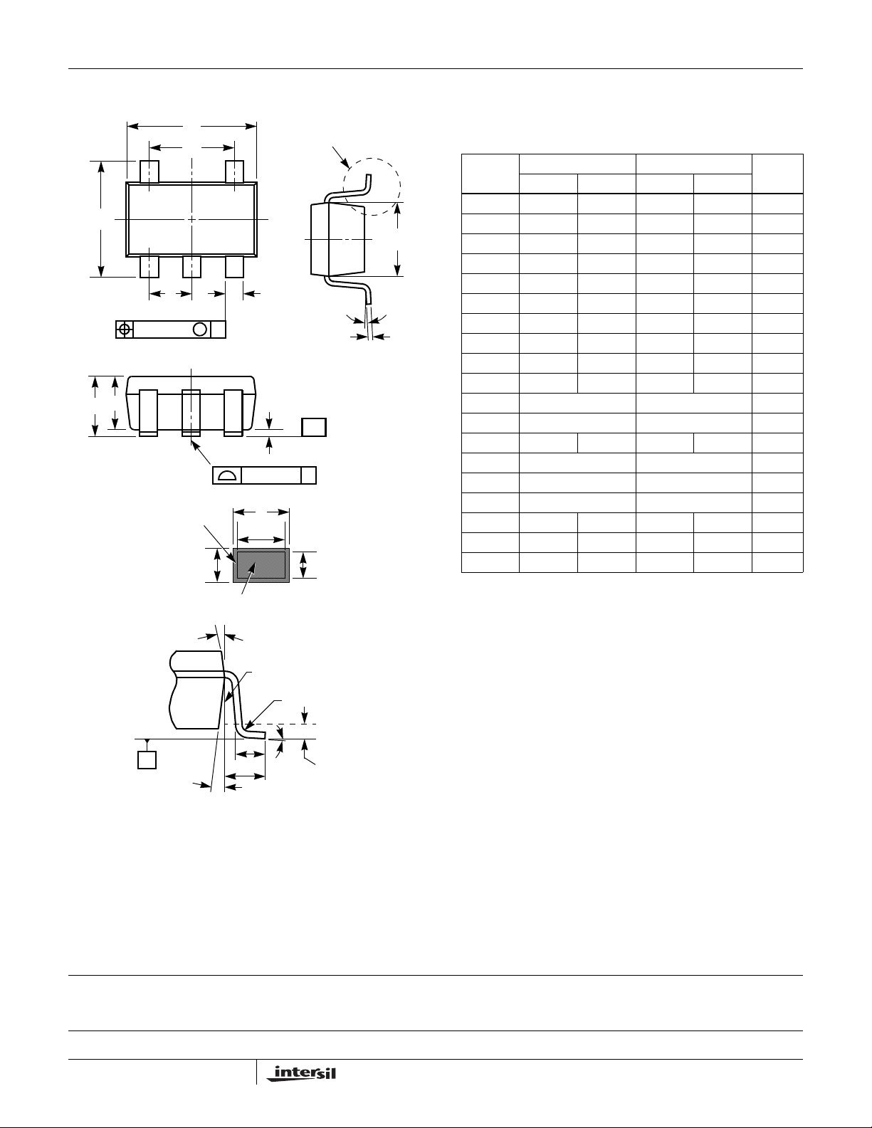
Small Outline Transistor Plastic Packages (SOT23-5)
E
A2
A
SEATING
PLANE
D
e1
123
C
L
C
L
c
BASE METAL
b
e
0.20 (0.008) M
C
WITH
PLATING
4X θ1
C
4X θ1
45
C
L
A1
0.10 (0.004) C
b
b1
R1
R
L
α
L1
VIEW C
C
L
SEATING
PLANE
-C-
c1
GAUGE PLANE
L2
P5.064
5 LEAD SMALL OUTLINE TRANSISTOR PLASTIC PACKAGE
INCHES MILLIMETERS
SYMBOL
A 0.036 0.057 0.90 1.45 -
A1 0.000 0.0059 0.00 0.15 -
E1
A2 0.036 0.051 0.90 1.30 -
b 0.012 0.020 0.30 0.50 -
b1 0.012 0.018 0.30 0.45
c 0.003 0.009 0.08 0.22 6
α
C
c1 0.003 0.008 0.08 0.20 6
D 0.111 0.118 2.80 3.00 3
E 0.103 0.118 2.60 3.00 -
E1 0.060 0.067 1.50 1.70 3
e 0.0374 Ref 0.95 Ref -
e1 0.0748 Ref 1.90 Ref -
L 0.014 0.022 0.35 0.55 4
L1 0.024 Ref. 0.60 Ref.
L2 0.010 Ref. 0.25 Ref.
N5 55
R 0.004 - 0.10 -
R1 0.004 0.010 0.10 0.25
o
α
0
o
8
o
0
NOTES:
1. Dimensioning and tolerance per ASME Y14.5M-1994.
2. Package conforms to EIAJ SC-74 and JEDEC MO178AA.
3. Dimensions D and E1 are exclusive of mold flash, protrusions,
or gate burrs.
4. Footlength L measured at reference to gauge plane.
5. “N” is the number of terminal positions.
6. These Dimensions apply to the flat section of the lead between
0.08mm and 0.15mm from the lead tip.
7. Controlling dimension: MILLIMETER. Converted inch dimensions are for reference only.
o
8
NOTESMIN MAX MIN MAX
-
Rev. 2 9/03
VIEW C
All Intersil U.S. products are manufactured, assembled and tested utilizing ISO9000 quality systems.
Intersil Corporation’s quality certifications can be viewed at www.intersil.com/design/quality
Intersil products are sold by description only. Intersil Corporation reserves the right to make changes in circuit design, software and/or specifications at any time without
notice. Accordingly, the reader is cautioned to verify that data sheets are current before placing orders. Information furnished by Intersil is believed to be accurate and
reliable. However, no responsibility is assumed by Intersil or its subsidiaries for its use; nor for any infringements of patents or other rights of third parties which may result
from its use. No license is granted by implicat ion or oth erwise u nde r any p a tent or p at ent r ights of Intersil or its subsidiaries.
For information regarding Intersil Corporation and its products, see www.intersil.com
12
FN8093.1
December 14, 2006
 Loading...