®
http://www.BDTIC.com/Intersil
ISL8560MREP
Data Sheet
DC/DC Power Switching Regulator
The ISL8560MREP is a step down DC/DC power switching
regulator which accepts 9.0V to 60V input and provides a 2A
output current. The output voltage can be set in the range
between 1.21V and 55V by means of an external divider.
The device uses an internal power DMOS transistor with a
typical r
of 0.19Ω to obtain very high efficiency and
DS(ON)
high switching speed. A switching frequency in the range of
100kHz to 600kHz can be realized (the maximum power
dissipation of the various packages must be observed).
Notable features of this next generation of DC/DC converter
includes pulse-by-pulse current limit for FET protection,
hiccup mode for short circuit protection, voltage feedforward
regulation, Frequency SYNC, soft-start, low standby current
of 60µA typical in the disabled state, and thermal shut-down.
The device is available in a 20 Ld QFN package.
Device Information
The specifications for an Enhanced Product (EP) device are
defined in a Vendor Item Drawing (VID), which is controlled
by the Defense Supply Center in Columbus (DSCC).
“Hot-links” to the applicable VID and other supporting
application information are provided on our website.
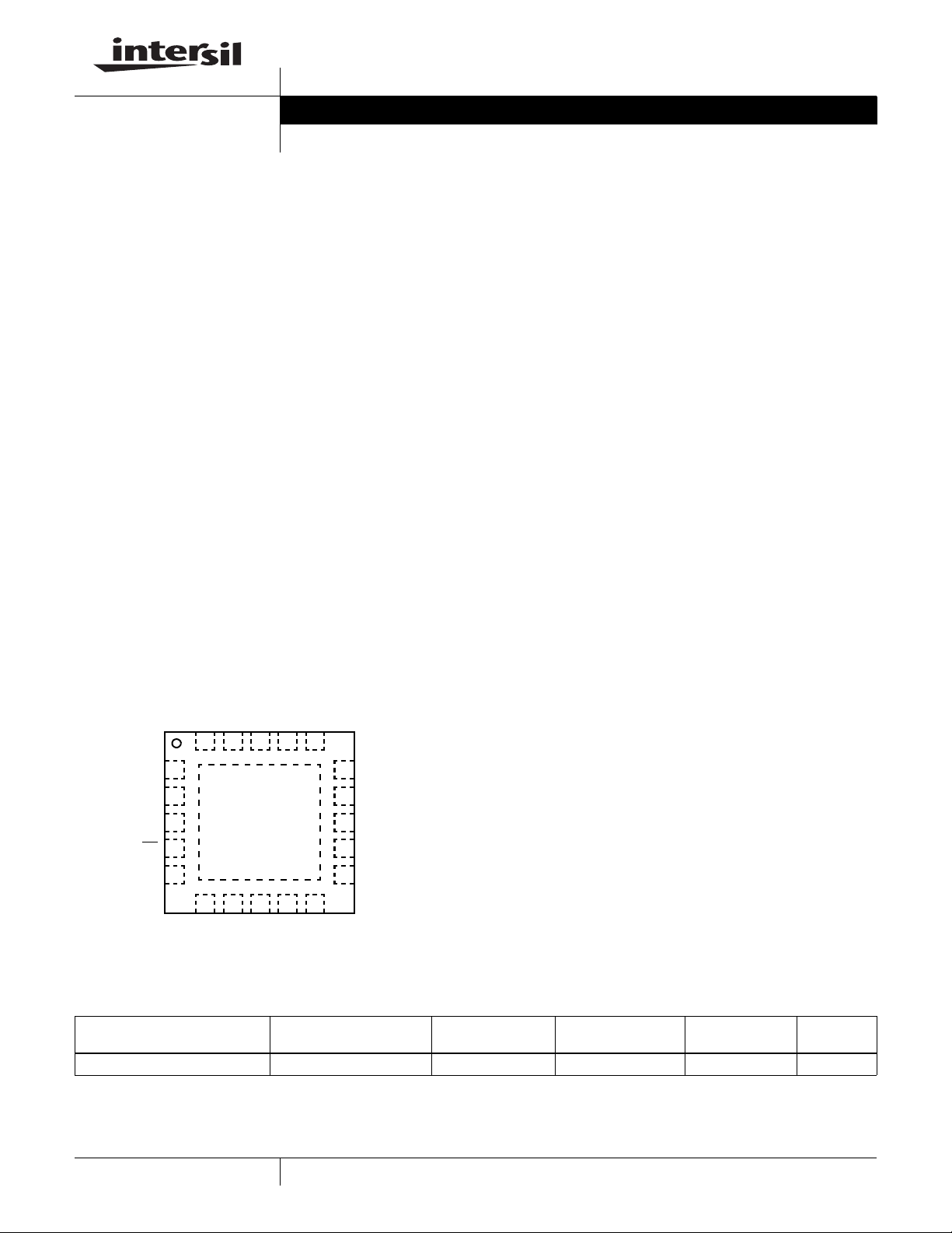
Pinout
ISL8560MREP
(20 LD QFN)
TOP VIEW
LX
VIN
VIN
VIN
VIN
20 19 18 17 16
LX
LX
BOOT
EN
VCC5
1
2
3
4
5
678910
RTCT
SYNC
SGND
FB
15
14
13
12
11
COMP
LX
SS
PGND
PGOOD
REF
December 13, 2007
FN6621.0
Features
• Specifications per DSCC VID V62/08608
• Full Mil-Temp Electrical Performance from -55°C to +125°C
• Controlled Baseline with One Wafer Fabrication Site and
One Assembly/Test Site
• Full Homogeneous Lot Processing in Wafer Fab
• No Combination of Wafer Fabrication Lots in Assembly
• Full Traceability Through Assembly and Test by
Date/Trace Code Assignment
• Enhanced Process Change Notification
• Enhanced Obsolescence Management
• Eliminates Need for Up-Screening a COTS Component
• Voltage Feedforward Mode
• Step Down DC/DC Supporting up to 2A Based on Max T
and VIN/VOUT
• Input Voltage Range of 9.0V to 60V
• Internal Reference of 1.21V ±1%
• Adjustable Output Voltage Range of 1.21V to 55V
• Adjustable Switching Frequency 100kHz to 600kHz
• Frequency SYNC Pin
• Zero Load Current Operation
• Pulse by Pulse Mode Current Limit and Hiccup mode
• Low Standby Current of 60µA Typical
• Thermal Shut-down
• Load Dump to 100V for 400ms
Applications
• Industrial and Avionics power supplies
• Portable computers
• Battery chargers
• Distributed power systems
Related Literature
• Technical Brief TB363 “Guidelines for Handling and
Processing Moisture Sensitive Surface Mount Devices
(SMDs)”
J
Ordering Information
VENDOR PART NUMBER
(Notes 1, 2) VENDOR ITEM DRAWING
ISL8560MREP V62/08608-01XB ISL8560MREP -55 to +125 20 Ld 6x6 QFN L20.6x6B
NOTES:
1. Refer to TB347 for details on reel specifications.
2. Devices must be procured to the VENDOR PART NUMBER.
1
CAUTION: These devices are sensitive to electrostatic discharge; follow proper IC Handling Procedures.
1-888-INTERSIL or 1-888-468-3774
PART
MARKING
TEMP.
RANGE (°C) PACKAGE PKG. DWG. #
| Intersil (and design) is a registered trademark of Intersil Americas Inc.
All other trademarks mentioned are the property of their respective owners.
Copyright Intersil Americas Inc. 2007. All Rights Reserved

ISL8560MREP
http://www.BDTIC.com/Intersil
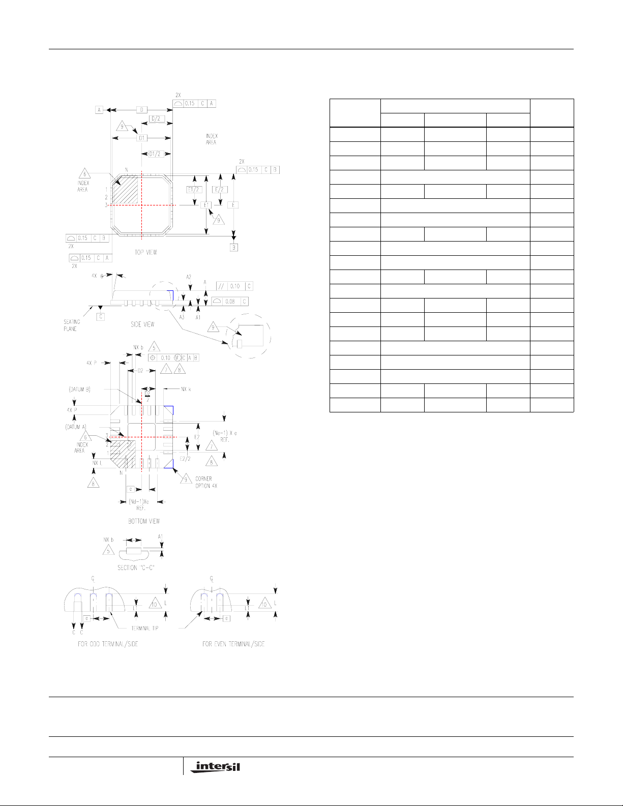
Quad Flat No-Lead Plastic Package (QFN)
Micro Lead Frame Plastic Package (MLFP)
L20.6x6B
20 LEAD QUAD FLAT NO-LEAD PLASTIC PACKAGE
(COMPLIANT TO JEDEC MO-220VJJB ISSUE C)
MILLIMETERS
SYMBOL
A 0.80 0.90 1.00 A1 - - 0.05 A2 - - 1.00 9
A3 0.20 REF 9
b 0.28 0.33 0.38 5, 8
D 6.00 BSC D1 5.75 BSC 9
D2 3.33 3.43 3.53 7, 8
E 6.00 BSC E1 5.75 BSC 9
E2 3.33 3.43 3.53 7, 8
e 0.80 BSC -
k 0.635 - - -
L 0.50 0.60 0.70 8
L1 - - 0.15 10
N202
Nd 5 3
Ne 5 3
P- -0.609
θ --129
NOTES:
1. Dimensioning and tolerancing conform to ASME Y14.5-1994.
2. N is the number of terminals.
3. Nd and Ne refer to the number of terminals on each D and E.
4. All dimensions are in millimeters. Angles are in degrees.
5. Dimension b applies to the metallized terminal and is measured
between 0.15mm and 0.30mm from the terminal tip.
6. The configuration of the pin #1 identifier is optional, but must be
located within the zone indicated. The pin #1 identifier may be
either a mold or mark feature.
7. Dimensions D2 and E2 are for the exposed pads which provide
improved electrical and thermal performance.
8. Nominal dimensions are provided to assist with PCB Land
Pattern Design efforts, see Intersil Technical Brief TB389.
9. Features and dimensions A2, A3, D1, E1, P & θ are present when
Anvil singulation method is used and not present for saw
singulation.
10. Depending on the method of lead termination at the edge of the
package, a maximum 0.15mm pull back (L1) maybe present.
L minus L1 to be equal to or greater than 0.3mm.
NOTESMIN NOMINAL MAX
Rev. 0 12/04
All Intersil U.S. products are manufactured, assembled and tested utilizing ISO9000 quality systems.
Intersil Corporation’s quality certifications can be viewed at www.intersil.com/design/quality
Intersil products are sold by description only. Intersil Corporation reserves the right to make changes in circuit design, software and/or specifications at any time without
notice. Accordingly, the reader is cautioned to verify that data sheets are current before placing orders. Information furnished by Intersil is believed to be accurate and
reliable. However, no responsibility is assumed by Intersil or its subsidiaries for its use; nor for any infringements of patents or other rights of third parties which may result
from its use. No license is granted by implic atio n or other wise u nde r any p a tent or patent rights of Intersil or its subsidiaries.
For information regarding Intersil Corporation and its products, see www.intersil.com
2
FN6621.0
 Loading...