

查询ISL8483IB供应商
®
ISL8483, ISL8485, ISL8488,
ISL8489, ISL8490, ISL8491
Data Sheet December 2003
5V, Low Power, High Speed or Slew Rate
Limited, RS-485/RS-422 Transceivers
The Intersil RS-485/RS-422 devices are BiCMOS 5V
powered, single transceivers that meet both the RS-485 and
RS-422 standards for balanced communication. Unlike
competitive devices, this Intersil family is specified for 10%
tolerance supplies (4.5V to 5.5V).
The ISL8483, ISL8488, and ISL8489 utilize slew rate limited
drivers which reduce EMI, and minimize reflections from
improperly terminated transmission lines, or unterminated
stubs in multidrop and multipoint applications.
Data rates up to 5Mbps are achievable by using the
ISL8485, ISL8490, or ISL8491, which feature higher slew
rates.
All devices present a “single unit load” to the RS-485 bus,
which allows up to 32 transceivers on the network.
Receiver (Rx) inputs feature a “fail-safe if open” design,
which ensures a logic high Rx output if Rx inputs are
floating.
Driver (Tx) outputs are short circuit protected, even for
voltages exceeding the power supply voltage. Additionally,
on-chip thermal shutdown circuitry disables the Tx outputs to
prevent damage if power dissipation becomes excessive.
The ISL8488 - 91 are configured for full duplex (separate Rx
input and Tx output pins) applications. The ISL8488 and
ISL8490 are offered in space saving 8 lead packages for
applications not requiring Rx and Tx output disable functions
(e.g., point-to-point). Half duplex configurations (ISL8483,
ISL8485) multiplex the Rx inputs and Tx outputs to allow
transceivers with Rx and Tx disable functions in 8 lead
packages.
FN6046.3
Features
• Specified for 10% Tolerance Supplies
• Class 3 ESD Protection (HBM) on all Pins. . . . . . . . >7kV
• High Data Rates. . . . . . . . . . . . . . . . . . . . . . up to 5Mbps
• Slew Rate Limited Versions for Error Free Data
Transmission at 250kbps (ISL8483, ISL8488, ISL8489)
• Single Unit Load Allows up to 32 Devices on the Bus
• 1nA Low Current Shutdown Mode (ISL8483)
• Low Quiescent Current:
µA (ISL8483, ISL8488, ISL8489)
-160
µA (ISL8485, ISL8490, ISL8491)
-340
• -7V to +12V Common Mode Input Voltage Range
• Three State Rx and Tx Outputs (Except ISL8488,
ISL8490)
• 30ns Propagation Delays, 5ns Skew (ISL8485, ISL8490,
ISL8491)
• Full Duplex and Half Duplex Pinouts
• Operate from a Single +5V Supply (10% Tolerance)
• Current Limiting and Thermal Shutdown for driver
Overload Protection
Applications
• Factory Automation
• Security Networks
• Building Environmental Control Systems
• Industrial/Process Control Networks
• Level Translators (e.g., RS-232 to RS-422)
• RS-232 “Extension Cords”
TABLE 1. SUMMARY OF FEATURES
PART
NUMBER
ISL8483 Half 32 0.25 Yes Yes 160 Yes 8
ISL8485 Half 32 5 No Yes 340 No 8
ISL8488 Full 32 0.25 Yes No 160 No 8
ISL8489 Full 32 0.25 Yes Yes 160 No 14
ISL8490 Full 32 5 No No 340 No 8
ISL8491 Full 32 5 No Yes 340 No 14
HALF/FULL
DUPLEX
NO. OF DEVICES
ALLOWED ON BUS
1
DATA RATE
(Mbps)
SLEW-RATE
LIMITED?
CAUTION: These devices are sensitive to electrostatic discharge; follow proper IC Handling Procedures.
1-888-INTERSIL or 321-724-7143
RECEIVER/
DRIVER ENABLE?
| Intersil (and design) is a registered trademark of Intersil Americas Inc.
All other trademarks mentioned are the property of their respective owners.
QUIESCENT
I
(µA)
CC
Copyright © Intersil Americas Inc. 2003. All Rights Reserved.
LOW POWER
SHUTDOWN?
PIN
COUNT
ISL8483, ISL8485, ISL8488, ISL8489, ISL8490, ISL8491
Ordering Information
PART NO.
(BRAND)
ISL8483IB
(8483IB)
ISL8483IB-T
(8483IB)
ISL8483IP -40 to 85 8 Ld PDIP E8.3
ISL8485CB
(8485CB)
ISL8485CB-T
(8485CB)
ISL8485CP 0 to 70 8 Ld PDIP E8.3
ISL8485IB
(8485IB)
ISL8485IB-T
(8485IB)
ISL8485IP -40 to 85 8 Ld PDIP E8.3
ISL8488IB
(8488IB)
ISL8488IB-T
(8488IB)
ISL8488IP -40 to 85 8 Ld PDIP E8.3
ISL8489IB -40 to 85 14 Ld SOIC M14.15
ISL8489IB-T -40 to 85 14 Ld SOIC
TEMP.
RANGE (
o
C) PACKAGE PKG. DWG. #
-40 to 85 8 Ld SOIC M8.15
-40 to 85 8 Ld SOIC
Tape and Reel
0 to 70 8 Ld SOIC M8.15
0 to 70 8 Ld SOIC
Tape and Reel
-40 to 85 8 Ld SOIC M8.15
-40 to 85 8 Ld SOIC
Tape and Reel
-40 to 85 8 Ld SOIC M8.15
-40 to 85 8 Ld SOIC
Tape and Reel
Tape and Reel
M8.15
M8.15
M8.15
M8.15
M14.15
Pinouts
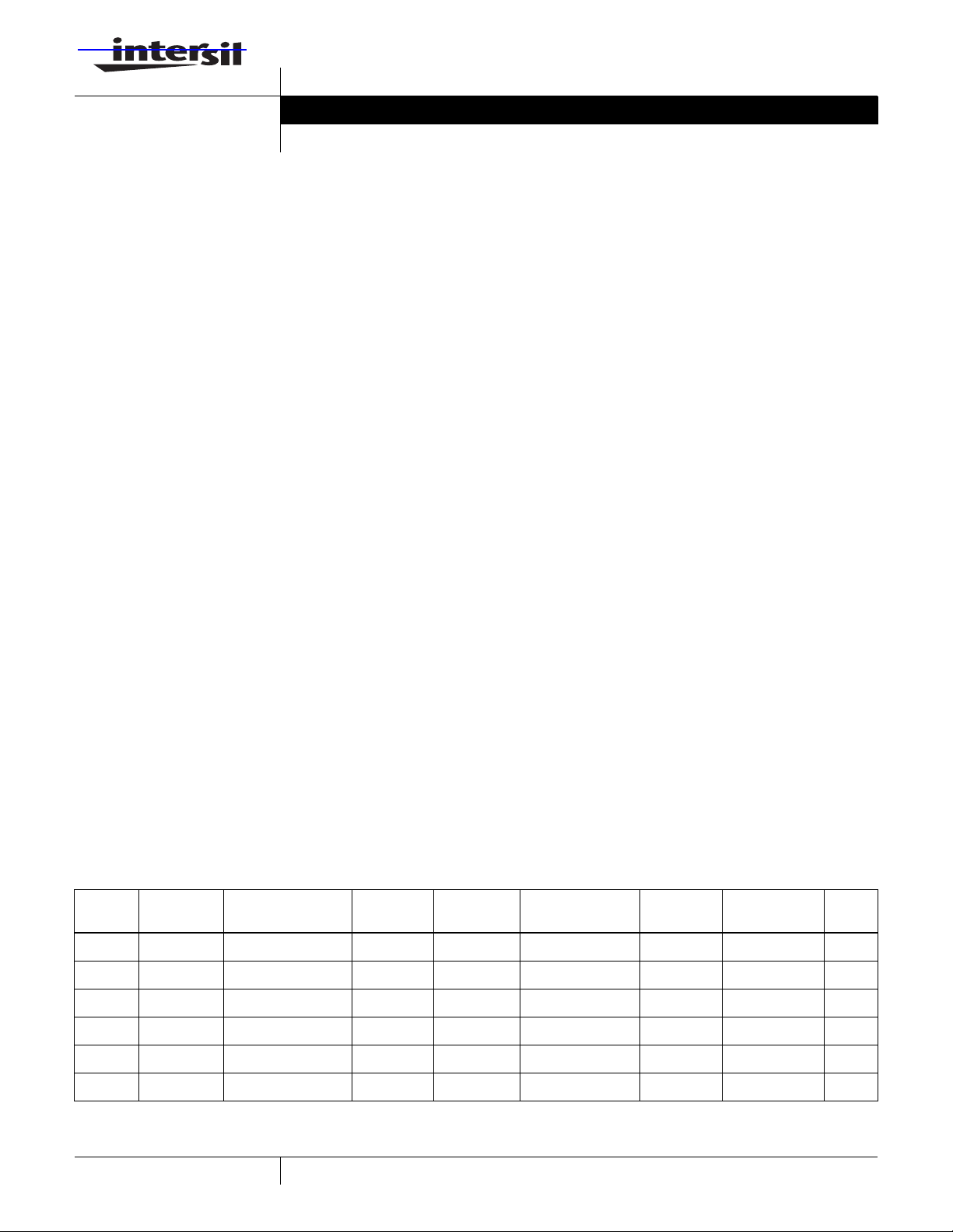
ISL8483, ISL8485 (PDIP, SOIC)
TOP VIEW
RO
RE
DE
1
R
2
3
D
4
DI
8
V
CC
7
B/Z
A/Y
6
GND
5
ISL8488, ISL8490 (PDIP, SOIC)
TOP VIEW
V
CC
RO
GND
1
R
2
DI
3
D
4
8
A
7
B
Z
6
Y
5
ISL8489, ISL8491 (PDIP, SOIC)
TOP VIEW
NC
RO
RE
DE
GND
GND
1
2
R
3
4
DI
D
5
6
7
V
14
CC
NC
13
A
12
B
11
Z
10
9
Y
8
NC
ISL8489IP -40 to 85 14 Ld PDIP E14.3
ISL8490IB
-40 to 85 8 Ld SOIC M8.15
(8490IB)
ISL8490IB-T
(8490IB)
-40 to 85 8 Ld SOIC
Tape and Reel
M8.15
ISL8490IP -40 to 85 8 Ld PDIP E8.3
ISL8491IB -40 to 85 14 Ld SOIC M14.15
ISL8491IB-T -40 to 85 14 Ld SOIC
M14.15
Tape and Reel
ISL8491IP -40 to 85 14 Ld PDIP E14.3
2
ISL8483, ISL8485, ISL8488, ISL8489, ISL8490, ISL8491
Truth Tables
TRANSMITTING
INPUTS OUTPUTS
RE
X1101
X1010
0 0 X High-Z High-Z
1 0 X High-Z * High-Z *
*Shutdown Mode for ISL8483 (see Note 7)
DE DI Z Y
RE
00X≥ +0.2V 1
00X≤ -0.2V 0
0 0 X Inputs Open 1
100XHigh-Z *
111XHigh-Z
*Shutdown Mode for ISL8483 (see Note 7)
DE
Half DuplexDEFull Duplex
RECEIVING
INPUTS OUTPUT
A-B RO
Pin Descriptions
PIN FUNCTION
RO Receiver output: If A > B by at least 0.2V, RO is high; If A < B by 0.2V or more, RO is low; RO = High if A and B are unconnected (floating).
RE
DE Driver output enable. The driver outputs, Y and Z, are enabled by bringing DE high. They are high impedance when DE is low.
DI Driver input. A low on DI forces output Y low and output Z high. Similarly, a high on DI forces output Y high and output Z low.
GND Ground connection.
A/Y Noninverting receiver input and noninverting driver output. Pin is an input (A) if DE = 0; pin is an output (Y) if DE = 1.
B/Z Inverting receiver input and inverting driver output. Pin is an input (B) if DE = 0; pin is an output (Z) if DE = 1.
V
NC No Connection.
Receiver output enable. RO is enabled when RE is low; RO is high impedance when RE is high.
A Noninverting receiver input.
B Inverting receiver input.
Y Noninverting driver output.
Z Inverting driver output.
System power supply input (4.5V to 5.5V).
CC
3

ISL8483, ISL8485, ISL8488, ISL8489, ISL8490, ISL8491
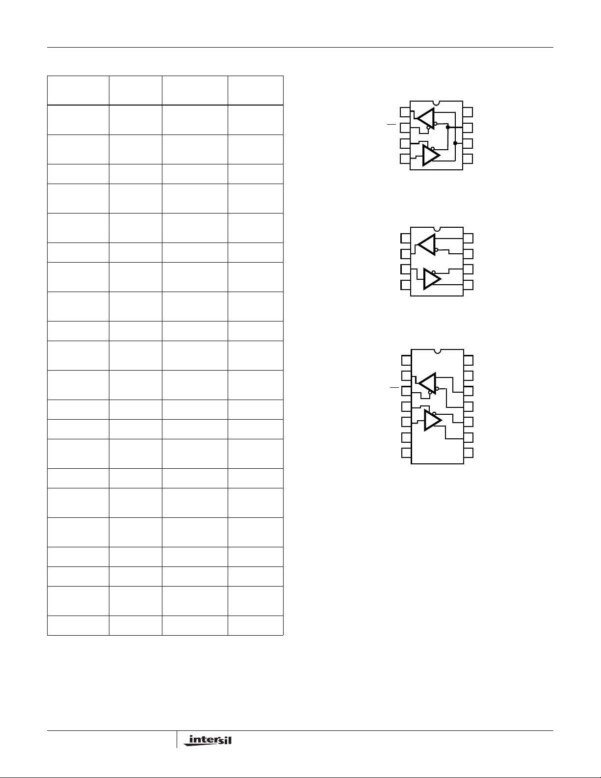
Typical Operating Circuits
+5V
ISL8483, ISL8485
+5V
+
8
V
CC
RO
1
2
3
4
RE
DE
DI
R
B/Z
A/Y
D
GND
5
0.1µF
R
7
6
T
R
0.1µF
T
+
8
V
CC
4
DI
D
7
B/Z
6
A/Y
R
GND
5
DE
RE
RO
3
2
1
ISL8488, ISL8490
+5V
+
1
V
CC
RO
2
R
A
B
0.1µF
8
7
R
T
0.1µF
+
+5V
1
V
CC
Y
5
Z
6
D
3
DI
6
GND
Z
5
Y
4
DI
3
D
R
T
B
7
A
8
R
GND
4
RO
2
ISL8489, ISL8491
+5V
+
14
V
CC
2
RO
R
3
RE
4
DE
5
DI
D
A
B
Z
Y
GND
6, 7
0.1µF
12
11
10
9
R
T
R
T
0.1µF
+
10
11
12
+5V
14
V
CC
Y
9
Z
B
A
GND
6, 7
DI
DE
RE
RO
5
4
3
2
D
R
4
ISL8483, ISL8485, ISL8488, ISL8489, ISL8490, ISL8491
Absolute Maximum Ratings Thermal Information
VCC to Ground. . . . . . . . . . . . . . . . . . . . . . . . . . . . . . . . . . . . . . . 7V
Input Voltages
DI, DE, RE
. . . . . . . . . . . . . . . . . . . . . . . . . . -0.5V to (VCC +0.5V)
Input/Output Voltages
A, B, Y, Z . . . . . . . . . . . . . . . . . . . . . . . . . . . . . . . . -8V to +12.5V
RO . . . . . . . . . . . . . . . . . . . . . . . . . . . . . . . . -0.5V to (V
CC
+0.5V)
Short Circuit Duration
Y, Z. . . . . . . . . . . . . . . . . . . . . . . . . . . . . . . . . . . . . . . Continuous
ESD Rating
HBM (Per MIL-STD-883, Method 3015.7) . . . . . . . . . . . . . . >7kV
Thermal Resistance (Typical, Note 1)
8 Ld SOIC Package . . . . . . . . . . . . . . . . . . . . . . . . . 170
8 Ld PDIP Package . . . . . . . . . . . . . . . . . . . . . . . . . 140
14 Ld SOIC Package . . . . . . . . . . . . . . . . . . . . . . . . 120
14 Ld PDIP Package . . . . . . . . . . . . . . . . . . . . . . . . 100
Moisture Sensitivity (see Technical Brief TB363)
All Packages . . . . . . . . . . . . . . . . . . . . . . . . . . . . . . . . . . . Level 1
Maximum Junction Temperature (Plastic Package) . . . . . . . 150
Maximum Storage Temperature Range . . . . . . . . . -65
Maximum Lead Temperature (Soldering 10s). . . . . . . . . . . . 300
(SOIC - Lead Tips Only)
Operating Conditions
Temperature Range
ISL84XXCX . . . . . . . . . . . . . . . . . . . . . . . . . . . . . . . . 0
ISL84XXIX . . . . . . . . . . . . . . . . . . . . . . . . . . . . . . . -40
CAUTION: Stresses above those listed in “Absolute Maximum Ratings” may cause permanent damage to the device. This is a stress only rating and operation of the
device at these or any other conditions above those indicated in the operational sections of this specification is not implied.
NOTE:
is measured with the component mounted on a low effective thermal conductivity test board in free air. See Tech Brief TB379 for details.
1. θ
JA
o
C to 70oC
o
C to 85oC
θ
(oC/W)
JA
o
C to 150oC
o
o
C
C
Electrical Specifications Test Conditions: V
Typicals are at V
PARAMETER SYMBOL TEST CONDITIONS
DC CHARACTERISTICS
Driver Differential V
Driver Differential V
Change in Magnitude of Driver
Differential V
OUT
Complementary Output States
Driver Common-Mode V
Change in Magnitude of Driver
Common-Mode V
Complementary Output States
Logic Input High Voltage V
Logic Input Low Voltage V
Logic Input Current I
Input Current (A, B), Note 10 I
Receiver Differential Threshold
Voltage
Receiver Input Hysteresis ∆V
Receiver Output High Voltage V
Receiver Output Low Voltage V
Three-State (high impedance)
Receiver Output Current
(no load) V
OUT
(with load) V
OUT
for
OUT
for
OUT
∆V
V
∆V
I
I
V
I
OZR
OD1
OD2
OD
OC
OC
IH
IL
IN1
IN1
IN1
IN2
TH
TH
OH
OL
R = 50Ω (RS-422), Figure 1 Full 2 3 - V
R = 27Ω (RS-485), Figure 1 Full 1.5 2.3 5 V
R = 27Ω or 50Ω, Figure 1 Full - 0.01 0.2 V
R = 27Ω or 50Ω, Figure 1 Full - - 3 V
R = 27Ω or 50Ω, Figure 1 Full - 0.01 0.2 V
DE, DI, RE Full 2 - - V
DE, DI, RE Full - - 0.8 V
DE, DI, RE (ISL8483) Full -2 - 2 µA
DI (ISL8485 - ISL8491) Full -2 - 2 µA
DE, RE (ISL8485, ISL8489, ISL8491) Full -25 - 25 µA
DE = 0V, VCC = 0V or
4.5 to 5.5V
-7V ≤ VCM ≤ 12V Full -0.2 - 0.2 V
VCM = 0V 25 - 70 - mV
IO = -4mA, VID = 200mV Full 3.5 - - V
IO = -4mA, VID = 200mV Full - - 0.4 V
0.4V ≤ VO ≤ 2.4V Full - - ±1 µA
= 4.5V to 5.5V; Unless Otherwise Specified.
CC
= 5V, TA = 25oC, Note 2
CC
VIN = 12V Full - - 1 mA
V
= -7V Full - - -0.8 mA
IN
TEMP
o
C) MIN TYP MAX UNITS
(
Full - - V
CC
V
5

ISL8483, ISL8485, ISL8488, ISL8489, ISL8490, ISL8491
Electrical Specifications Test Conditions: V
Typicals are at V
= 4.5V to 5.5V; Unless Otherwise Specified.
CC
= 5V, TA = 25oC, Note 2 (Continued)
CC
PARAMETER SYMBOL TEST CONDITIONS
Receiver Input Resistance R
No-Load Supply Current, Note 3 I
CC
-7V ≤ VCM ≤ 12V Full 12 - - kΩ
IN
ISL8488, ISL8489, DE, DI, RE = 0V or V
ISL8490, ISL8491, DE, DI, RE
ISL8485, DI, RE
V
CC
ISL8483, DI, RE
V
CC
Shutdown Supply Current I
Driver Short-Circuit Current,
V
= High or Low
O
Receiver Short-Circuit Current I
SHDN
I
OSD1
OSR
ISL8483, DE = 0V, RE = VCC, DI = 0V or V
DE = VCC, -7V ≤ VY or VZ ≤ 12V, Note 4 Full 35 - 250 mA
0V ≤ VO ≤ V
SWITCHING CHARACTERISTICS (ISL8485, ISL8490, ISL8491)
Driver Input to Output Delay t
Driver Output Skew t
Driver Differential Rise or Fall Time t
Driver Enable to Output High t
Driver Enable to Output Low t
Driver Disable from Output High t
Driver Disable from Output Low t
Receiver Input to Output Delay t
Receiver Skew | t
PLH
- t
|t
PHL
Receiver Enable to Output High t
Receiver Enable to Output Low t
Receiver Disable from Output High t
Receiver Disable from Output Low t
Maximum Data Rate f
PLH
PLH
, t
SKEW
, t
R
ZH
ZL
HZ
LZ
, t
SKD
ZH
ZL
HZ
LZ
MAX
PHLRDIFF
F
= 54Ω, CL = 100pF, Figure 2 Full 18 30 50 ns
R
= 54Ω, CL = 100pF, Figure 2 Full - 2 10 ns
DIFF
R
= 54Ω, CL = 100pF, Figure 2 Full 3 11 25 ns
DIFF
CL = 100pF, SW = GND, Figure 3 Full - 17 70 ns
CL = 100pF, SW = VCC, Figure 3 Full - 14 70 ns
CL = 15pF, SW = GND, Figure 3 Full - 19 70 ns
CL = 15pF, SW = VCC, Figure 3 Full - 13 70 ns
Figure 4 Full 30 40 150 ns
PHL
Figure 4 25 - 5 - ns
CL = 15pF, SW = GND, Figure 5 Full - 9 50 ns
CL = 15pF, SW = VCC, Figure 5 Full - 9 50 ns
CL = 15pF, SW = GND, Figure 5 Full - 9 50 ns
CL = 15pF, SW = VCC, Figure 5 Full - 9 50 ns
SWITCHING CHARACTERISTICS (ISL8483, ISL8488, ISL8489)
Driver Input to Output Delay t
Driver Output Skew t
Driver Differential Rise or Fall Time t
Driver Enable to Output High t
Driver Enable to Output Low t
Driver Disable from Output High t
Driver Disable from Output Low t
Receiver Input to Output Delay t
- t
Receiver Skew | t
PLH
|t
PHL
Receiver Enable to Output High t
Receiver Enable to Output Low t
Receiver Disable from Output High t
PLH
PLH
, t
SKEW
, t
R
ZH
ZL
HZ
LZ
, t
SKD
ZH
ZL
HZ
PHLRDIFF
F
= 54Ω, CL = 100pF, Figure 2 Full 250 800 2000 ns
R
= 54Ω, CL = 100pF, Figure 2 Full - 160 800 ns
DIFF
R
= 54Ω, CL = 100pF, Figure 2 Full 250 800 2000 ns
DIFF
CL = 100pF, SW = GND, Figure 3, Note 5 Full 250 - 2000 ns
CL = 100pF, SW = VCC, Figure 3, Note 5 Full 250 - 2000 ns
CL = 15pF, SW = GND, Figure 3 Full 300 - 3000 ns
CL = 15pF, SW = VCC, Figure 3 Full 300 - 3000 ns
Figure 4 Full 250 350 2000 ns
PHL
Figure 4 25 - 25 - ns
CL = 15pF, SW = GND, Figure 5, Note 6 Full - 10 50 ns
CL = 15pF, SW = VCC, Figure 5, Note 6 Full - 10 50 ns
CL = 15pF, SW = GND, Figure 5 Full - 10 50 ns
CC
= 0V or
= 0V or
TEMP
o
(
C) MIN TYP MAX UNITS
Full - 160 250 µA
Full - 340 500 µA
Full - 550 900 µA
= 0V or V
DE = V
CC
CC
CC
DE = 0V Full - 340 500 µA
DE = V
CC
Full - 390 650 µA
DE = 0V Full - 160 250 µA
CC
Full - 1 50 nA
Full 7 - 85 mA
Full 5 - - Mbps
6

ISL8483, ISL8485, ISL8488, ISL8489, ISL8490, ISL8491
Electrical Specifications Test Conditions: V
Typicals are at V
PARAMETER SYMBOL TEST CONDITIONS
Receiver Disable from Output Low t
Maximum Data Rate f
Time to Shutdown (ISL8483 only) t
Driver Enable from Shutdown to
Output High (ISL8483 only)
Driver Enable from Shutdown to
LZ
MAX
SHDN
t
ZH(SHDN)CL
t
ZL(SHDN)CL
= 4.5V to 5.5V; Unless Otherwise Specified.
CC
= 5V, TA = 25oC, Note 2 (Continued)
CC
TEMP
o
(
C) MIN TYP MAX UNITS
CL = 15pF, SW = VCC, Figure 5 Full - 10 50 ns
Full 250 - - kbps
Note 7 Full 50 200 600 ns
= 100pF, SW = GND, Figure 3, Notes 7, 8 Full - - 2000 ns
= 100pF, SW = VCC, Figure 3, Notes 7, 8 Full - - 2000 ns
Output Low (ISL8483 only)
Receiver Enable from Shutdown to
Output High (ISL8483 only)
Receiver Enable from Shutdown to
Output Low (ISL8483 only)
t
ZH(SHDN)CL
t
ZL(SHDN)CL
= 15pF, SW = GND, Figure 5, Notes 7, 9 Full - - 2500 ns
= 15pF, SW = VCC, Figure 5, Notes 7, 9 Full - - 2500 ns
NOTES:
2. All currents into device pins are positive; all currents out of device pins are negative. All voltages are referenced to device ground unless
otherwise specified.
3. Supply current specification is valid for loaded drivers when DE = 0V.
4. Applies to peak current. See “Typical Performance Curves” for more information.
5. When testing the ISL8483, keep RE
6. When testing the ISL8483, the RE
7. The ISL8483 is put into shutdown by bringing RE
= 0 to prevent the device from entering SHDN.
signal high time must be short enough (typically <200ns) to prevent the device from entering SHDN.
high and DE low. If the inputs are in this state for less than 50ns, the parts are guaranteed not
to enter shutdown. If the inputs are in this state for at least 600ns, the parts are guaranteed to have entered shutdown. See “Low-Power
Shutdown Mode” section.
8. Keep RE
9. Set the RE
= VCC, and set the DE signal low time >600ns to ensure that the device enters SHDN.
signal high time >600ns to ensure that the device enters SHDN.
10. Devices meeting these limits are denoted as “single unit load (1 UL)” transceivers. The RS-485 standard allows up to 32 Unit Loads on the bus.
Test Circuits and Waveforms
DE
V
CC
DI
Z
D
Y
V
OD
FIGURE 1. DRIVER VOD AND V
R
OC
V
OC
R
7

ISL8483, ISL8485, ISL8488, ISL8489, ISL8490, ISL8491
Test Circuits and Waveforms (Continued)
CL = 100pF
= 100pF
C
L
V
CC
SIGNAL
GENERATOR
DE
DI
Z
D
Y
R
DIFF
FIGURE 2A. TEST CIRCUIT
FIGURE 2. DRIVER PROPAGATION DELAY AND DIFFERENTIAL TRANSITION TIMES
DE
DI
SIGNAL
GENERATOR
(SHDN) for ISL8483 only
Z
D
Y
500Ω
C
L
SW
V
GND
PARAMETER OUTPUT RE DI SW CL (pF)
t
HZ
t
LZ
t
ZH
t
ZL
t
ZH(SHDN)
t
ZL(SHDN)
Y/Z X 1/0 GND 15
Y/Z X 0/1 V
CC
15
Y/Z 0 (Note 5) 1/0 GND 100
Y/Z 0 (Note 5) 0/1 V
CC
100
Y/Z 1 (Note 8) 1/0 GND 100
Y/Z 1 (Note 8) 0/1 V
CC
100
CC
DI
OUT (Y)
OUT (Z)
DIFF OUT (Y - Z)
SKEW = |t
PLH
DE
tZH, t
ZH(SHDN)
NOTE 7
OUT (Y, Z)
t
, t
ZL
ZL(SHDN)
NOTE 7
OUT (Y, Z)
1.5V1.5V
t
PLH
50% 50%
t
PHL
50% 50%
90% 90%
10% 10%
t
R
(Y or Z) - t
PHL
(Z or Y)|
t
PHL
t
PLH
FIGURE 2B. MEASUREMENT POINTS
NOTE 7
OUTPUT HIGH
2.3V
2.3V
OUTPUT LOW
1.5V1.5V
t
HZ
t
LZ
VOH - 0.5V
VOL + 0.5V
3V
0V
V
OH
V
OL
V
OH
V
OL
+V
OD
-V
OD
t
F
3V
0V
V
OH
0V
V
CC
V
OL
FIGURE 3A. TEST CIRCUIT FIGURE 3B. MEASUREMENT POINTS
+1.5V
SIGNAL
GENERATOR
FIGURE 4A. TEST CIRCUIT
FIGURE 3. DRIVER ENABLE AND DISABLE TIMES (EXCLUDING ISL8488, ISL8490)
RE
B
A
RO
R
15pF
A
RO
t
PLH
50% 50%
FIGURE 4B. MEASUREMENT POINTS
FIGURE 4. RECEIVER PROPAGATION DELAY
8
t
1.5V1.5V
PHL
3V
0V
V
CC
0V

ISL8483, ISL8485, ISL8488, ISL8489, ISL8490, ISL8491
Test Circuits and Waveforms (Continued)
RE
B
SIGNAL
GENERATOR
(SHDN) for ISL8483 only.
PARAMETER DE A SW
t
HZ
t
LZ
tZH (Note 6) 0 +1.5V GND
(Note 6) 0 -1.5V V
t
ZL
t
ZH(SHDN)
t
ZL(SHDN)
(Note 9) 0 +1.5V GND
(Note 9) 0 -1.5V V
A
FIGURE 5A. TEST CIRCUIT
RO
R
0 +1.5V GND
0-1.5VV
FIGURE 5. RECEIVER ENABLE AND DISABLE TIMES (EXCLUDING ISL8488, ISL8490)
1kΩ
SW
15pF
V
GND
CC
CC
CC
CC
NOTE 7
RE
tZH, t
ZH(SHDN)
NOTE 7
RO
t
, t
ZL
ZL(SHDN)
NOTE 7
RO
FIGURE 5B. MEASUREMENT POINTS
OUTPUT HIGH
1.5V
1.5V
OUTPUT LOW
1.5V1.5V
t
HZ
t
LZ
3V
0V
VOH - 0.5V
VOL + 0.5V
V
OH
0V
V
CC
V
OL
Application Information
RS-485 and RS-422 are differential (balanced) data
transmission standards for use in long haul or noisy
environments. RS-422 is a subset of RS-485, so RS-485
transceivers are also RS-422 compliant. RS-422 is a pointto-multipoint (multidrop) standard, which allows only one
driver and up to 10 (assuming one unit load devices)
receivers on each bus. RS-485 is a true multipoint standard,
which allows up to 32 one unit load devices (any
combination of drivers and receivers) on each bus. To allow
for multipoint operation, the RS-485 spec requires that
drivers must handle bus contention without sustaining any
damage.
Another important advantage of RS-485 is the extended
common mode range (CMR), which specifies that the driver
outputs and receiver inputs withstand signals that range
from +12V to -7V. RS-422 and RS-485 are intended for runs
as long as 4000’, so the wide CMR is necessary to handle
ground potential differences, as well as voltages induced in
the cable by external fields.
Receiver Features
These devices utilize a differential input receiver for maximum
noise immunity and common mode rejection. Input sensitivi ty
is ±200mV, as required by the RS422 and RS-485
specifications.
Receiver input impedance surpasses the RS-422 spec of
4kΩ, and meets the RS-485 “Unit Load” requirement of
12kΩ minimum.
Receiver inputs function with common mode voltages as
great as ±7V outside the power supplies (i.e., +12V and
-7V), making them ideal for long networks where induced
voltages are a realistic concern.
All the receivers include a “fail-safe if open” function that
guarantees a high level receiver output if the receiver inputs
are unconnected (floating).
Receivers easily meet the data rates supported by the
corresponding driver.
ISL8483/85/89/91 receiver outputs are three-statable via the
active low RE
input.
Driver Features
The RS-485/422 driver is a differential output device that
delivers at least 1.5Vacross a 54Ω load (RS-485), and at
least 2V across a 100Ω load (RS-422). The drivers feature
low propagation delay skew to maximize bit width, and to
minimize EMI.
Drivers of the ISL8483/85/89/91 are three-statable via the
active high DE input.
The ISL8483/88/89 driver outputs are slew rate limited to
minimize EMI, and to minimize reflections in unterminated or
improperly terminated networks. Data rate on these slew
rate limited versions is a maximum of 250kbps. Outputs of
ISL8485/90/91 drivers are not limited, so faster output
transition times allow data rates of at least 5Mbps.
Data Rate, Cables, and Terminations
RS-485/422 are intended for network lengths up to 4000’,
but the maximum system data rate decreases as the
transmission length increases. Devices operating at 5Mbps
are limited to lengths less than 100’, while the 250kbps
versions can operate at full data rates with lengths in excess
of 1000’.
Twisted pair is the cable of choice for RS-485/422 networks.
Twisted pair cables tend to pick up noise and other
electromagnetically induced voltages as common mode
signals, which are effectively rejected by the differential
receivers in these ICs.
Proper termination is imperative, when using the 5Mbps
devices, to minimize reflections. Short networks using the
250kbps versions need not be terminated, but, terminations
are recommended unless power dissipation is an overriding
concern.
9

ISL8483, ISL8485, ISL8488, ISL8489, ISL8490, ISL8491
In point-to-point, or point-to-multipoint (single driver on bus)
networks, the main cable should be terminated in its
characteristic impedance (typically 120Ω) at the end farthest
from the driver. In multi-receiver applications, stubs
connecting receivers to the main cable should be kept as
short as possible. Multipoint (multi-driver) systems require
that the main cable be terminated in its characteristic
impedance at both ends. Stubs connecting a transceiver to
the main cable should be kept as short as possible.
Built-In Driver Overload Protection
As stated previously, the RS-485 spec requires that drivers
survive worst case bus contentions undamaged. The
ISL84XX devices meet this requirement via driver output
short circuit current limits, and on-chip thermal shutdown
circuitry.
The driver output stages incorporate short circuit current
limiting circuitry which ensures that the output current never
exceeds the RS-485 spec, even at the common mode
voltage range extremes. Additionally, these devices utilize a
foldback circuit which reduces the short circuit current, and
thus the power dissipation, whenever the contending voltage
exceeds either supply.
Typical Performance Curves V
90
80
70
60
50
40
30
20
DRIVER OUTPUT CURRENT (mA)
10
0
012345
DIFFERENTIAL OUTPUT VOLTAGE (V)
FIGURE 6. DRIVER OUTPUT CURRENT vs DIFFERENTIAL
OUTPUT VOLTAGE
= 5V, TA = 25oC, ISL8483 thru ISL8491; Unless Otherwise Specified
CC
In the event of a major short circuit condition, ISL84XX
devices also include a thermal shutdown feature that
disables the drivers whenever the die temperature becomes
excessive. This eliminates the power dissipation, allowing
the die to cool. The drivers automatically reenable after the
die temperature drops about 15 degrees. If the contention
persists, the thermal shutdown/reenable cycle repeats until
the fault is cleared. Receivers stay operational during
thermal shutdown.
Low Power Shutdown Mode (ISL8483 Only)
These CMOS transceivers all use a fraction of the power
required by their bipolar counterparts, but the ISL8483
includes a shutdown feature that reduces the already low
quiescent I
whenever the receiver and driver are simultaneously
disabled (RE
600ns. Disabling both the driver and the receiver for less
than 50ns guarantees that the ISL8483 will not enter
shutdown.
Note that receiver and driver enable times increase when
the ISL8483 enables from shutdown. Refer to Notes 5-8, at
the end of the Electrical Specification table, for more
information.
DIFFERENTIAL OUTPUT VOLTAGE (V)
FIGURE 7. DRIVER DIFFERENTIAL OUTPUT VOLTAGE vs
to a 1nA trickle. The ISL8483 enters shutdown
CC
=VCC and DE = GND) for a period of at least
3.6
3.4
3.2
3
2.8
2.6
2.4
2.2
2
-40 0 50 85
-25 25 75
TEMPERATURE
R
= 100Ω
DIFF
TEMPERATURE (oC)
R
DIFF
= 54Ω
10

ISL8483, ISL8485, ISL8488, ISL8489, ISL8490, ISL8491
Typical Performance Curves V
160
140
120
100
80
60
40
20
0
-20
-40
-60
OUTPUT CURRENT (mA)
-80
-100
-120
-7 -6 -4 -2 0 2 4 6 8 10 12
Y OR Z = LOW
OUTPUT VOLTAGE (V)
= 5V, TA = 25oC, ISL8483 thru ISL8491; Unless Otherwise Specified (Continued)
CC
Y OR Z = HIGH
FIGURE 8. DRIVER OUTPUT CURRENT vs SHORT CIRCUIT
VOLTAGE
1200
1100
1000
t
PLHY
t
PLHZ
600
550
500
450
400
350
(µA)
CC
I
300
250
200
ISL8483, DE = GND, RE = GND; ISL8488/89, DE = RE = X
150
100
-40 0 50 85
ISL8485, DE = VCC, RE = X
ISL8483, DE = VCC, RE = X
ISL8485, DE = GND, RE = X
ISL8490/91, DE = RE = X
-25 25 75
TEMPERATURE (oC)
FIGURE 9. SUPPLY CURRENT vs TEMPERATURE
400
300
900
800
700
PROPAGATION DELAY (ns)
600
500
-40 0 50 85
-25 25 75
TEMPERATURE (oC)
FIGURE 10. DRIVER PROPAGATION DELAY vs
TEMPERATURE (ISL8483, ISL8488, ISL8489)
40
35
t
PHLY
t
PHLZ
30
25
PROPAGATION DELAY (ns)
t
PLHY
t
PLHZ
t
PHLY
t
PHLZ
|t
- t
PLHZ
|
|t
- t
PLHY
PHLZ
PHLY
200
SKEW (ns)
100
|CROSS PT. OF Y↑ & Z↓ - CROSS PT. OF Y↓ & Z↑|
0
-40 0 50 85
-25 25 75
TEMPERATURE (oC)
FIGURE 11. DRIVER SKEW vs TEMPERATURE
(ISL8483, ISL8488, ISL8489)
3
2.5
|t
- t
PLHZ
|
|t
- t
PLHY
PHLZ
PHLY
2
SKEW (ns)
1.5
|CROSSING PT. OF Y↑ & Z↓ - CROSSING PT. OF Y↓ & Z↑|
|
|
20
-40 0 50 85
-25 25 75
TEMPERATURE (oC)
FIGURE 12. DRIVER PROPAGATION DELAY vs
TEMPERATURE (ISL8485, ISL8490, ISL8491)
11
1
-40 0 50 85
-25 25 75
TEMPERATURE (oC)
FIGURE 13. DRIVER SKEW vs TEMPERATURE
(ISL8485, ISL8490, ISL8491)

ISL8483, ISL8485, ISL8488, ISL8489, ISL8490, ISL8491
Typical Performance Curves V
R
DIFF
DI
5
0
RECEIVER OUTPUT (V)
4
3
2
1
0
DRIVER OUTPUT (V)
RO
B/Z
A/Y
TIME (400ns/DIV)
CC
= 54Ω, CL = 100pF
FIGURE 14. DRIVER AND RECEIVER WAVEFORMS,
LOW TO HIGH (ISL8483, ISL8488, ISL8489)
R
= 54Ω, CL = 100pF
DIFF
DI
5
0
RECEIVER OUTPUT (V)
RO
= 5V, TA = 25oC, ISL8483 thru ISL8491; Unless Otherwise Specified (Continued)
R
= 54Ω, CL = 100pF
5
0
DRIVER INPUT (V)
5
0
RECEIVER OUTPUT (V)
4
3
2
1
0
DRIVER OUTPUT (V)
DI
RO
A/Y
B/Z
TIME (400ns/DIV)
DIFF
FIGURE 15. DRIVER AND RECEIVER WAVEFORMS,
HIGH TO LOW (ISL8483, ISL8488, ISL8489)
R
= 54Ω, CL = 100pF
5
0
DRIVER INPUT (V)
5
0
RECEIVER OUTPUT (V)
DI
RO
DIFF
5
0
DRIVER INPUT (V)
5
0
DRIVER INPUT (V)
4
3
2
1
0
DRIVER OUTPUT (V)
B/Z
A/Y
TIME (10ns/DIV)
FIGURE 16. DRIVER AND RECEIVER WAVEFORMS,
LOW TO HIGH (ISL8485, ISL8490, ISL8491)
Die Characteristics
SUBSTRATE POTENTIAL (POWERED UP):
GND
TRANSISTOR COUNT:
518
PROCESS:
Si Gate CMOS
4
A/Y
3
2
B/Z
1
0
DRIVER OUTPUT (V)
TIME (10ns/DIV)
FIGURE 17. DRIVER AND RECEIVER WAVEFORMS,
HIGH TO LOW (ISL8485, ISL8490, ISL8491)
12

ISL8483, ISL8485, ISL8488, ISL8489, ISL8490, ISL8491
Dual-In-Line Plastic Packages (PDIP)
N
D1
-C-
E1
-B-
A2
A
L
A
1
e
C
e
e
INDEX
AREA
BASE
PLANE
SEATING
PLANE
D1
B1
12 3 N/2
-AD
e
B
0.010 (0.25) C AM BS
NOTES:
1. Controlling Dimensions: INCH. In case of conflict between
English and Metric dimensions, the inch dimensions control.
2. Dimensioning and tolerancing per ANSI Y14.5M-1982.
3. Symbols are defined in the “MO Series Symbol List” in Section
2.2 of Publication No. 95.
4. Dimensions A, A1 and L are measured with the package seated
in JEDEC seating plane gauge GS-3.
5. D, D1, and E1 dimensions do not include mold flash or protrusions. Mold flash or protrusions shall not exceed 0.010 inch
(0.25mm).
6. E and are measured with the leads constrained to be per-
7. e
e
pendicular to datum .
A
and eC are measured at the lead tips with the leads uncon-
B
strained. e
must be zero or greater.
C
-C-
8. B1 maximum dimensions do not include dambar protrusions.
Dambar protrusions shall not exceed 0.010 inch (0.25mm).
9. N is the maximum number of terminal positions.
10. Corner leads (1, N, N/2 and N/2 + 1) for E8.3, E16.3, E18.3,
E28.3, E42.6 will have a B1 dimension of 0.030 - 0.045 inch
(0.76 - 1.14mm).
E8.3 (JEDEC MS-001-BA ISSUE D)
8 LEAD DUAL-IN-LINE PLASTIC PACKAGE
INCHES MILLIMETERS
SYMBOL
A - 0.210 - 5.33 4
E
A1 0.015 - 0.39 - 4
A2 0.115 0.195 2.93 4.95 -
B 0.014 0.022 0.356 0.558 -
C
L
A
C
B
B1 0.045 0.070 1.15 1.77 8, 10
C 0.008 0.014 0.204 0.355 D 0.355 0.400 9.01 10.16 5
D1 0.005 - 0.13 - 5
E 0.300 0.325 7.62 8.25 6
E1 0.240 0.280 6.10 7.11 5
e 0.100 BSC 2.54 BSC -
e
A
e
B
0.300 BSC 7.62 BSC 6
- 0.430 - 10.92 7
L 0.115 0.150 2.93 3.81 4
N8 89
NOTESMIN MAX MIN MAX
Rev. 0 12/93
13

ISL8483, ISL8485, ISL8488, ISL8489, ISL8490, ISL8491
Dual-In-Line Plastic Packages (PDIP)
N
D1
-C-
E1
-B-
A1
A2
E
A
L
e
C
C
L
e
A
C
e
B
INDEX
AREA
BASE
PLANE
SEATING
PLANE
D1
B1
12 3 N/2
-AD
e
B
0.010 (0.25) C AM BS
NOTES:
1. Controlling Dimensions: INCH. In case of conflict between English
and Metric dimensions, the inch dimensions control.
2. Dimensioning and tolerancing per ANSI Y14.5M-1982.
3. Symbols are defined in the “MO Series Symbol List” in Section 2.2 of
Publication No. 95.
4. Dimensions A, A1 and L are measured with the package seated in
JEDEC seating plane gauge GS-3.
5. D, D1, and E1 dimensions do not include mold flash or protrusions.
Mold flash or protrusions shall not exceed 0.010 inch (0.25mm).
6. E and are measured with the leads constrained to be perpen-
7. e
e
dicular to datum .
A
and eC are measured at the lead tips with the leads uncon-
B
strained. e
-C-
must be zero or greater.
C
8. B1 maximum dimensions do not include dambar protrusions. Dambar
protrusions shall not exceed 0.010 inch (0.25mm).
9. N is the maximum number of terminal positions.
10. Corner leads (1, N, N/2 and N/2 + 1) for E8.3, E16.3, E18.3, E28.3,
E42.6 will have a B1 dimension of 0.030 - 0.045 inch (0.76 -
1.14mm).
E14.3 (JEDEC MS-001-AA ISSUE D)
14 LEAD DUAL-IN-LINE PLASTIC PACKAGE
INCHES MILLIMETERS
SYMBOL
A - 0.210 - 5.33 4
A1 0.015 - 0.39 - 4
A2 0.115 0.195 2.93 4.95 -
B 0.014 0.022 0.356 0.558 B1 0.045 0.070 1.15 1.77 8
C 0.008 0.014 0.204 0.355 -
D 0.735 0.775 18.66 19.68 5
D1 0.005 - 0.13 - 5
E 0.300 0.325 7.62 8.25 6
E1 0.240 0.280 6.10 7.11 5
e 0.100 BSC 2.54 BSC e
A
e
B
0.300 BSC 7.62 BSC 6
- 0.430 - 10.92 7
L 0.115 0.150 2.93 3.81 4
N14 149
NOTESMIN MAX MIN MAX
Rev. 0 12/93
14

ISL8483, ISL8485, ISL8488, ISL8489, ISL8490, ISL8491
Small Outline Plastic Packages (SOIC)
N
INDEX
AREA
123
SEATING PLANE
-AD
e
B
0.25(0.010) C AM BS
M
E
-B-
A
-C-
0.25(0.010) BM M
H
α
µ
A1
0.10(0.004)
L
h x 45
o
C
NOTES:
1. Symbols are defined in the “MO Series Symbol List” in Section 2.2 of
Publication Number 95.
2. Dimensioning and tolerancing per ANSI Y14.5M-1982.
3. Dimension “D” does not include mold flash, protrusions or gate burrs.
Mold flash, protrusion and gate burrs shall not exceed 0.15mm (0.006
inch) per side.
4. Dimension “E” does not include interlead flash or protrusions. Interlead flash and protrusions shall not exceed 0.25mm (0.010 inch) per
side.
5. The chamfer on the body is optional. If it is not present, a visual index
feature must be located within the crosshatched area.
6. “L” is the length of terminal for soldering to a substrate.
7. “N” is the number of terminal positions.
8. Terminal numbers are shown for reference only.
9. The lead width “B”, as measured 0.36mm (0.014 inch) or greater
above the seating plane, shall not exceed a maximum value of
0.61mm (0.024 inch).
10. Controlling dimension: MILLIMETER. Converted inch dimensions
are not necessarily exact.
M8.15 (JEDEC MS-012-AA ISSUE C)
8 LEAD NARROW BODY SMALL OUTLINE PLASTIC
PACKAGE
INCHES MILLIMETERS
SYMBOL
A 0.0532 0.0688 1.35 1.75 -
A1 0.0040 0.0098 0.10 0.25 -
B 0.013 0.020 0.33 0.51 9
C 0.0075 0.0098 0.19 0.25 D 0.1890 0.1968 4.80 5.00 3
E 0.1497 0.1574 3.80 4.00 4
e 0.050 BSC 1.27 BSC -
H 0.2284 0.2440 5.80 6.20 -
h 0.0099 0.0196 0.25 0.50 5
L 0.016 0.050 0.40 1.27 6
N8 87
o
α
0
o
8
o
0
o
8
Rev. 0 12/93
NOTESMIN MAX MIN MAX
-
15

ISL8483, ISL8485, ISL8488, ISL8489, ISL8490, ISL8491
Small Outline Plastic Packages (SOIC)
N
INDEX
AREA
123
SEATING PLANE
-AD
e
B
0.25(0.010) C AM BS
M
E
-B-
A
-C-
0.25(0.010) BM M
H
α
µ
A1
0.10(0.004)
L
h x 45
o
C
NOTES:
1. Symbols are defined in the “MO Series Symbol List” in Section 2.2 of
Publication Number 95.
2. Dimensioning and tolerancing per ANSI Y14.5M-1982.
3. Dimension “D” does not include mold flash, protrusions or gate burrs.
Mold flash, protrusion and gate burrs shall not exceed 0.15mm (0.006
inch) per side.
4. Dimension “E” does not include interlead flash or protrusions. Interlead
flash and protrusions shall not exceed 0.25mm (0.010 inch) per side.
5. The chamfer on the body is optional. If it is not present, a visual index
feature must be located within the crosshatched area.
6. “L” is the length of terminal for soldering to a substrate.
7. “N” is the number of terminal positions.
8. Terminal numbers are shown for reference only.
9. The lead width “B”, as measured 0.36mm (0.014 inch) or greater
above the seating plane, shall not exceed a maximum value of
0.61mm (0.024 inch).
10. Controlling dimension: MILLIMETER. Converted inch dimensions
are not necessarily exact.
M14.15 (JEDEC MS-012-AB ISSUE C)
14 LEAD NARROW BODY SMALL OUTLINE PLASTIC
PACKAGE
INCHES MILLIMETERS
SYMBOL
A 0.0532 0.0688 1.35 1.75 -
A1 0.0040 0.0098 0.10 0.25 -
B 0.013 0.020 0.33 0.51 9
C 0.0075 0.0098 0.19 0.25 D 0.3367 0.3444 8.55 8.75 3
E 0.1497 0.1574 3.80 4.00 4
e 0.050 BSC 1.27 BSC H 0.2284 0.2440 5.80 6.20 h 0.0099 0.0196 0.25 0.50 5
L 0.016 0.050 0.40 1.27 6
N14 147
o
α
0
o
8
o
0
o
8
Rev. 0 12/93
NOTESMIN MAX MIN MAX
-
All Intersil U.S. products are manufactured, assembled and tested utilizing ISO9000 quality systems.
Intersil Corporation’s quality certifications can be viewed at www.intersil.com/design/quality
Intersil products are sold by description only. Intersil Corporation reserves the right to make changes in circuit design, software and/or specifications at any time without
notice. Accordingly, the reader is cautioned to verify that data she ets are current before placin g orders. Information furn ished by Intersil is believed to be accurate and
reliable. However, no responsibility is assumed by Intersil or its subsidiaries for its use; nor for any infringements of patents or other rights of third parties which may result
from its use. No license is granted by implication or othe rwise under any patent or patent rights of Intersil or its subsidiaries.
For information regarding Intersil Corporation and its products, see www.intersil.com
16
 Loading...