

查询ISL84762供应商
®
ISL84762
Data Sheet November 30, 2004
Ultra Low ON-Resistance, Low Voltage,
Single Supply, Dual SPDT Analog Switch
The Intersil ISL84762 device is a low ON-resistance, low
voltage, bidirectional, dual single-pole/double-throw (SPDT)
analog switch designed to operate from a single +1.65V to
+3.6V supply. Targeted applications include battery powered
equipment that benefit from low R
switching speeds (t
ON
=14ns, t
input is 1.8V logic-compatible when using a single +3V supply.
Cell phones, for example, often face ASIC functionality
limitations. The number of analog input or GPIO pins may be
limited and digital geometries are not well suited to analog
switch performance. This part may be used to “mux-in”
additional functionality while reducing ASIC design risk. The
ISL84762 is offered in small form factor packages, alleviating
board space limitations.
The ISL84762 is a committed dual single-pole/double-throw
(SPDT) that consist of two normally open (NO) and two
normally (NC) switches. This configuration can be used as a
dual 2-to-1 multiplexer. The ISL84762 is pin compatible with
the MAX4762.
(0.35Ω) and fast
ON
= 6ns). The digital logic
OFF
FN6105.0
Features
• Pb-Free Available (RoHS Compliant) (see Ordering Info)
• Pin Compatible Replacement for the MAX4762
• ON Resistance (RON)
- V+ = +2.7V . . . . . . . . . . . . . . . . . . . . . . . . . . . . . 0.39Ω
- V+ = +1.8V . . . . . . . . . . . . . . . . . . . . . . . . . . . . . 0.55Ω
•RON Matching Between Channels. . . . . . . . . . . . . . . . 0.05Ω
Flatness Across Signal Range . . . . . . . . . . . . . 0.043Ω
•R
ON
• Single Supply Operation. . . . . . . . . . . . . . . . +1.65V to +3.6V
• Low Power Consumption (PD . . . . . . . . . . . . . . . . . <0.02µW
• Fast Switching Action (V+ = +2.7V)
. . . . . . . . . . . . . . . . . . . . . . . . . . . . . . . . . . . . 14ns
-t
ON
-t
. . . . . . . . . . . . . . . . . . . . . . . . . . . . . . . . . . . . 6ns
OFF
• ESD HBM Rating . . . . . . . . . . . . . . . . . . . . . . . . . . . . . . >9kV
• Guaranteed Break-before-Make
• 1.8V Logic Compatible (+3V supply)
• Available in 10 lead 3x3 Thin DFN and 10 lead MSOP
TABLE 1. FEATURES AT A GLANCE
ISL84762
Number of Switches 2
SW SPDT or 2-1 MUX
3V R
ON
3V t
ON/tOFF
1.8V R
ON
1.8V t
ON/tOFF
Packages 10 Ld 3x3 Thin DFN, 10 Ld MSOP
0.35Ω
12ns/5ns
0.55Ω
20ns/8ns
Related Literature
• Technical Brief TB363 “Guidelines for Handling and
Processing Moisture Sensitive Surface Mount Devices
(SMDs)”
• Application Note AN557 “Recommended Test Procedures
for Analog Switches”
Applications
• Battery powered, Handheld, and Portable Equipment
- Cellular/mobile Phones
- Pagers
- Laptops, Notebooks, Palmtops
• Portable Test and Measurement
• Medical Equipment
• Audio and Video Switching
1
CAUTION: These devices are sensitive to electrostatic discharge; follow proper IC Handling Procedures.
1-888-INTERSIL or 321-724-7143
| Intersil (and design) is a registered trademark of Intersil Americas Inc.
All other trademarks mentioned are the property of their respective owners.
Copyright Intersil Americas Inc. 2004. All Rights Reserved
ISL84762
Pinout (Note 1)
ISL84762 (TDFN, MSOP)
TOP VIEW
NO2
10
9
COM2
NC2
8
7
IN2
6
GND
NO1
COM1
NC1
IN1
V+
1
2
3
4
5
NOTE:
1. Switches Shown for Logic “0” Input.
Truth Table
LOGIC PIN NC1 and NC2 PIN NO1 and NO2
0ONOFF
1OFFON
NOTE: Logic “0” ≤0.5V. Logic “1” ≥1.4V with a 3V supply.
Pin Descriptions
PIN FUNCTION
V+ System Power Supply Input (+1.65V to +3.6V)
GND Ground Connection
IN Digital Control Input
COM Analog Switch Common Pin
NO Analog Switch Normally Open Pin
NC Analog Switch Normally Closed Pin
Ordering Information
PART NO.
(BRAND)
ISL84762IR
(762)
ISL84762IR-T
(762)
ISL84762IU
(4762)
ISL84762IU-T
(4762)
ISL84762IRZ
(762)
(See Note)
ISL84762IRZ-T
(762)
(See Note)
ISL84762IUZ
(4762)
(See Note)
ISL84762IUZ-T
(4762)
(See Note)
NOTE: Intersil Pb-free products employ special Pb-free material sets;
molding compounds/die attach materials and 100% matte tin plate
termination finish, which are RoHS compliant and compatible with
both SnPb and Pb-free soldering operations. Intersil Pb-free products
are MSL classified at Pb-free peak reflow temperatures that meet or
exceed the Pb-free requirements of IPC/JEDEC J STD-020C.
TEMP.
RANGE (°C) PACKAGE
PKG.
DWG. #
-40 to 85 10 Ld 3x3 Thin DFN L10.3x3A
-40 to 85 10 Ld 3x3 Thin DFN
L10.3x3A
Tape and Reel
-40 to 85 10 Ld MSOP M10.118
-40 to 85 10 Ld MSOP
M10.118
Tape and Reel
-40 to 85 10 Ld 3x3 Thin DFN
L10.3x3A
(Pb-free)
-40 to 85 10 Ld 3x3 Thin DFN
L10.3x3A
Tape and Reel
(Pb-free)
-40 to 85 10 Ld MSOP
M10.118
(Pb-free)
-40 to 85 10 Ld MSOP
M10.118
Tape and Reel
(Pb-free)
2
FN6105.0
November 30, 2004
ISL84762
Absolute Maximum Ratings Thermal Information
V+ to GND . . . . . . . . . . . . . . . . . . . . . . . . . . . . . . . . . . . -0.3 to 4.7V
Input Voltages
NO, NC, IN (Note 2). . . . . . . . . . . . . . . . . . . . . -0.3 to ((V+) + 0.3V)
Output Voltages
COM (Note 2). . . . . . . . . . . . . . . . . . . . . . . . . . -0.3 to ((V+) + 0.3V)
Continuous Current NO, NC, or COM . . . . . . . . . . . . . . . . . ±300mA
Peak Current NO, NC, or COM
(Pulsed 1ms, 10% Duty Cycle, Max) . . . . . . . . . . . . . . . . . . ±500mA
ESD Rating:
HBM . . . . . . . . . . . . . . . . . . . . . . . . . . . . . . . . . . . . . . . . . . . . .>9kV
MM. . . . . . . . . . . . . . . . . . . . . . . . . . . . . . . . . . . . . . . . . . . . . .>500V
CDM. . . . . . . . . . . . . . . . . . . . . . . . . . . . . . . . . . . . . . . . . . . . . .>1kV
CAUTION: Stresses above those listed in “Absolute Maximum Ratings” may cause permanent damage to the device. This is a stress only rating and operation of the
device at these or any other conditions above those indicated in the operational sections of this specification is not implied.
NOTES:
2. Signals on NC , NO , IN, or COM exceeding V+ or GND are clamped by internal diodes. Limit forward diode current to maximum current ratings.
is measured with the component mounted on a low effective thermal conductivity test board in free air. See Tech Brief TB379 for details.
3. θ
JA
Thermal Resistance (Typical) θ
(°C/W)
JA
10 Ld 3x3 TDFN Package (Note 3) . . . . . . . . . . . . . 110
10 Ld MSOP Package (Note 3) . . . . . . . . . . . . . . . . 190
Maximum Junction Temperature (Plastic Package). . . . . . . . 150°C
Maximum Storage Temperature Range . . . . . . . . . . . . . -65°C to 150°C
Maximum Lead Temperature (Soldering 10s) . . . . . . . . . . . . 300°C
(MSOP - Lead Tips Only)
Operating Conditions
Temperature Range. . . . . . . . . . . . . . . . . . . . . . . . . . -40°C to 85°C
Electrical Specifications - 3V Supply Test Conditions: V+ = +2.7V to +3.3V, GND = 0V, V
Unless Otherwise Specified
PARAMETER TEST CONDITIONS
ANALOG SWITCH CHARACTERISTICS
Analog Signal Range, V
ON Resistance, R
R
Matching Between Channels,
ON
∆R
ON
R
Flatness, R
ON
ON
FLAT(ON)
ANALOG
V+ = 2.7V, I
See Figure 5
V+ = 2.7V, I
max R
ON
, Note 9
V+ = 2.7V, I
= 100mA, VNO or VNC = 0V to V+,
COM
= 100mA, VNO or V
COM
= 100mA, VNO or VNC = 0V to V+,
COM
Note 7
NO or NC OFF Leakage Current,
I
NO(OFF)
or I
NC(OFF)
COM ON Leakage Current,
I
COM(ON)
V+ = 3.3V, V
V+ = 3.3V, V
or Floating
= 0.3V, 3V, VNO or VNC = 3V, 0.3V 25 -2 - 2 nA
COM
= 0.3V, 3V, or VNO or VNC = 0.3V, 3V,
COM
DYNAMIC CHARACTERISTICS
Turn-O N Ti me, t
ON
V+ = 2.7V, VNO or VNC = 1.5V, RL = 50Ω, CL = 35pF,
See Figure 1, Note 8
Turn-O FF Tim e, t
OFF
Break-Before-Make Time Delay, t
Charge Injection, Q C
OFF Isolation R
Crosstalk (Channel-to-Channel) R
V+ = 2.7V, VNO or VNC = 1.5V, RL = 50Ω, CL = 35pF,
See Figure 1, Note 8
V+ = 3.3V, VNO or VNC = 1.5V, RL = 50Ω, CL = 35pF,
D
See Figure 3, Note 8
= 1.0nF, VG = 0V, RG = 0Ω, See Figure 2 25 - 95 - pC
L
= 50Ω, CL = 5pF, f = 100kHz, V
L
See Figure 4
= 50Ω, CL = 5pF, f = 100kHz, V
L
See Figure 6
Total Harmonic Distortion f = 20Hz to 20kHz, V
NO or NC OFF Capacitance, C
COM ON Capacitance, C
COM(ON)
f = 1MHz, VNO or VNC = V
OFF
f = 1MHz, VNO or VNC = V
COM
TEMP
= Voltage at
NC
= 1V
COM
= 1V
COM
= 2V
, RL = 600Ω 25 - 0.003 - %
P-P
= 0V, See Figure 7 25 - 115 - pF
COM
= 0V, See Figure 7 25 - 224 - pF
COM
RMS
RMS
,
,
(NOTE 5)
(°C)
Full 0 - V+ V
25 - 0.39 0.6 Ω
Full - - 0.6 Ω
25 - 0.05 0.2 Ω
Full - - 0.2 Ω
25 - 0.043 0.1 Ω
Full - - 0.15 Ω
Full -40 - 40 nA
25 -3 - 3 nA
Full -60 - 60 nA
25 - 14 20 ns
Full - - 25 ns
25 - 6 12 ns
Full - - 17 ns
Full 2 7 - ns
25 - -68 - dB
25 - -95 - dB
= 1.4V, V
INH
MIN TYP
= 0.5V (Notes 4, 6),
INL
(NOTE 5)
MAX UNITS
3
FN6105.0
November 30, 2004
ISL84762
Electrical Specifications - 3V Supply Test Conditions: V+ = +2.7V to +3.3V, GND = 0V, V
= 1.4V, V
INH
= 0.5V (Notes 4, 6),
INL
Unless Otherwise Specified (Continued)
TEMP
PARAMETER TEST CONDITIONS
(°C)
(NOTE 5)
MIN TYP
(NOTE 5)
MAX UNITS
POWER SUPPLY CHARACTERISTICS
Power Supply Range Full 1.65 3.6 V
Positive Supply Current, I+ V+ = +3.6V, V
= 0V or V+ 25 - - 40 nA
IN
Full - - 750 nA
DIGITAL INPUT CHARACTERISTICS
Input Voltage Low, V
Input Voltage High, V
Input Current, I
INH
, I
INL
INH
INL
V+ = 3.3V, VIN = 0V or V+, Note 8 Full -0.5 - 0.5 µA
Full - - 0.5 V
Full 1.4 - - V
NOTES:
= input voltage to perform proper function.
4. V
IN
5. The algebraic convention, whereby the most negative value is a minimum and the most positive a maximum, is used in this data sheet.
6. Parts are 100% tested at +25°C. Limits across the full temperature range are guaranteed by design and correlation.
7. Flatness is defined as the difference between maximum and minimum value of on-resistance over the specified analog signal range.
8. Guaranteed but not tested.
matching between channels is calculated by subtracting the channel with the highest max Ron value from the channel with lowest max Ron
9. R
ON
value.
Electrical Specifications - 1.8V Supply Test Conditions: V+ = +1.65V to +2V, GND = 0V, V
= 1.0V, V
INH
= 0.4V (Note 4, 6),
INL
Unless Otherwise Specified
TEMP
PARAMETER TEST CONDITIONS
(°C)
(NOTE 5)
MIN TYP
(NOTE 5)
MAX UNITS
ANALOG SWITCH CHARACTERISTICS
Analog Signal Range, V
ON Resistance, R
ON
ANALOG
V+ = 1.8V, I
See Figure 5, Note 8
= 100mA, VNO or VNC = 0V to V+,
COM
Full 0 - V+ V
25 - 0.55 - Ω
Full - 0.6 - Ω
DYNAMIC CHARACTERISTICS
Turn-O N Ti me, t
Turn-O FF Tim e, t
ON
OFF
Break-Before-Make Time Delay, t
Charge Injection, Q C
OFF Isolation R
Crosstalk (Channel-to-Channel) R
NO or NC OFF Capacitance, C
COM ON Capacitance, C
COM(ON)
V+ = 1.65V, VNO or VNC = 1.0V, RL =50Ω, CL = 35pF,
See Figure 1, Note 8
V+ = 1.65V, VNO or VNC = 1.0V, RL =50Ω, CL = 35pF,
See Figure 1, Note 8
V+ = 2.0V, VNO or VNC = 1.0V, RL =50Ω, CL = 35pF,
D
See Figure 3, Note 8
= 1.0nF, VG = 0V, RG = 0Ω, See Figure 2 25 - 49 - pC
L
= 50Ω, CL = 5pF, f = 100kHz, V
L
See Figure 4
= 50Ω, CL = 5pF, f = 100kHz, V
L
See Figure 6
f = 1MHz, VNO or VNC = V
OFF
f = 1MHz, VNO or VNC = V
COM
COM
= 0V, See Figure 7 25 - 115 - pF
COM
= 0V, See Figure 7 25 - 224 - pF
COM
= 1V
= 1V
RMS
RMS
25 - 22 28 ns
Full - - 33 ns
25 - 9 15 ns
Full - - 20 ns
Full 2 9 - ns
,
,
25 - -68 - dB
25 - -95 - dB
DIGITAL INPUT CHARACTERISTICS
Input Voltage Low, V
Input Voltage High, V
Input Current, I
INH
, I
INL
INH
INL
V+ = 2.0V, VIN = 0V or V+, Note 8 Full -0.5 - 0.5 µA
Full - - 0.4 V
Full 1.0 - - V
4
FN6105.0
November 30, 2004

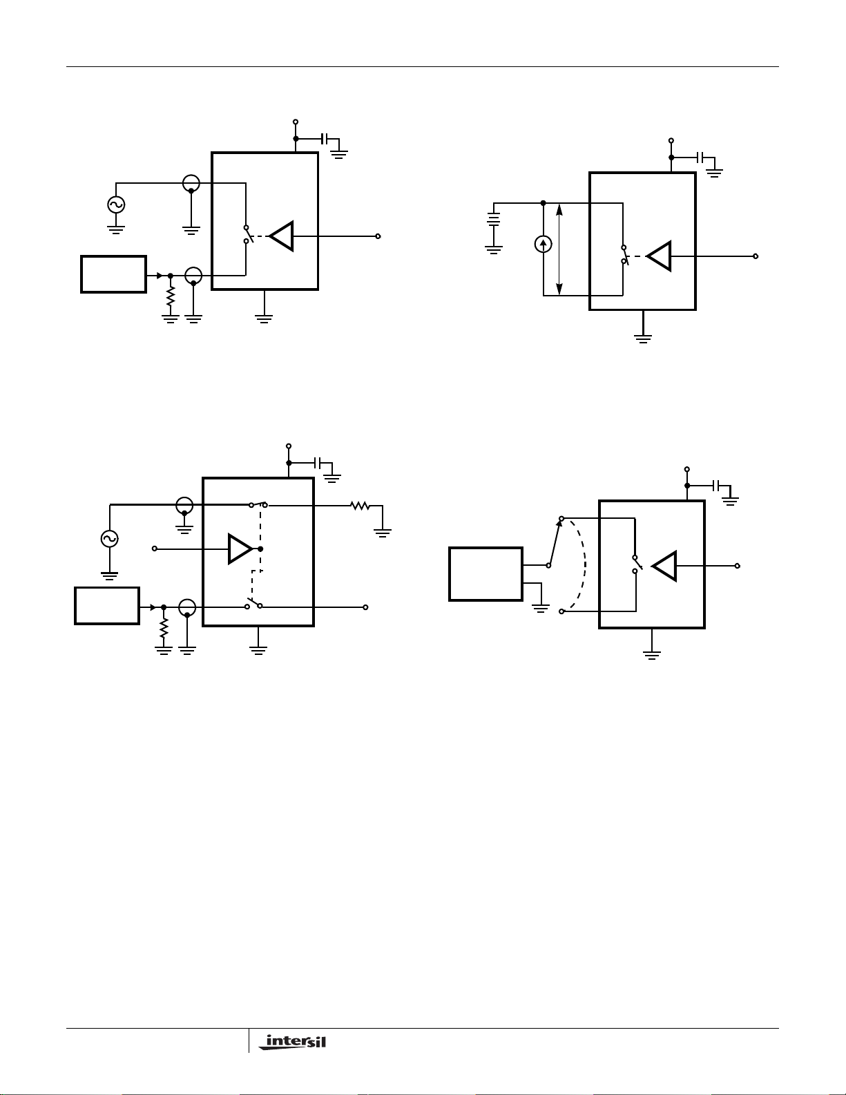
Test Circuits and Waveforms
V+
LOGIC
INPUT
SWITCH
INPUT
SWITCH
OUTPUT
0V
V
NO
0V
t
ON
50%
90%
t
OFF
V
OUT
Logic input waveform is inverted for switches that have the opposite
logic sense.
tr < 5ns
< 5ns
t
f
90%
ISL84762
SWITCH
LOGIC
INPUT
INPUT
NO or NC
IN
Repeat test for all switches. C
capacitance.
V
OUT
V
=
(NO or NC)
V+
C
COM
R
RL
50Ω
L
ON()
GND
includes fixture and stray
L
------------------------------
RLR
+
V
OUT
C
35pF
L
SWITCH
OUTPUT
V
LOGIC
INPUT
LOGIC
INPUT
SWITCH
OUTPUT
V
OUT
FIGURE 1A. MEASUREMENT POINTS
∆V
OUT
OUT
ON
Q = ∆V
OUT
x C
OFF
L
FIGURE 2A. MEASUREMENT POINTS
V+
0V
0V
t
D
FIGURE 3A. MEASUREMENT POINTS
FIGURE 1. SWITCHING TIMES
V
G
ON
V+
0V
Repeat test for all switches.
FIGURE 2. CHARGE INJECTION
V
NX
90%
LOGIC
INPUT
Repeat test for all switches. C
capacitance.
FIGURE 3. BREAK-BEFORE-MAKE TIME
FIGURE 1B. TEST CIRCUIT
V+
C
R
G
NO or NC
GND
FIGURE 2B. TEST CIRCUIT
V+
NO
NC
IN
GND
includes fixture and stray
L
FIGURE 3B. TEST CIRCUIT
C
COM
IN
COM
LOGIC
INPUT
R
50Ω
V
OUT
C
L
V
OUT
C
L
L
35pF
5
FN6105.0
November 30, 2004
Test Circuits and Waveforms (Continued)
V+
C
SIGNAL
GENERATOR
ANALYZER
R
L
NO or NC
COM
GND
IN
0V or V+
ISL84762
RON = V1/100mA
V
NX
100mA
V
1
NO or NC
COM
GND
V+
IN
C
0V or V+
Signal direction through switch is reversed, worst case values
are recorded. Repeat test for all switches.
FIGURE 4. OFF ISOLATION TEST CIRCUIT FIGURE 5. RON TEST CIRCUIT
V+
C
SIGNAL
GENERATOR
0V or V+
ANALYZER
R
L
Signal direction through switch is reversed, worst case values
are recorded. Repeat test for all switches.
NO or NC
IN
1
COM
COM
NC or NO
GND
50Ω
N.C.
FIGURE 6. CROSSTALK TEST CIRCUIT FIGURE 7. CAPACITANCE TEST CIRCUIT
Detailed Description
The ISL84762 is a bidirectional, dual single pole/double
throw (SPDT) analog switch that offers precise switching
capability from a single 1.65V to 3.6V supply with low onresistance (0.39Ω) and high speed operation (t
t
= 6ns). The device is especially well suited for portable
OFF
battery powered equipment due to its low operating supply
voltage (1.65V), low power consumption (2.7µW max), low
leakage currents (60nA max), and the tiny Thin DFN and
MSOP packages. The ultra low on-resistance and Ron
flatness provide very low insertion loss and distortion to
applications that require signal reproduction.
ON
= 14ns,
Repeat test for all switches.
V+
C
NO or NC
0V or V+
IN
IMPEDANCE
ANALYZER
COM
GND
Repeat test for all switches.
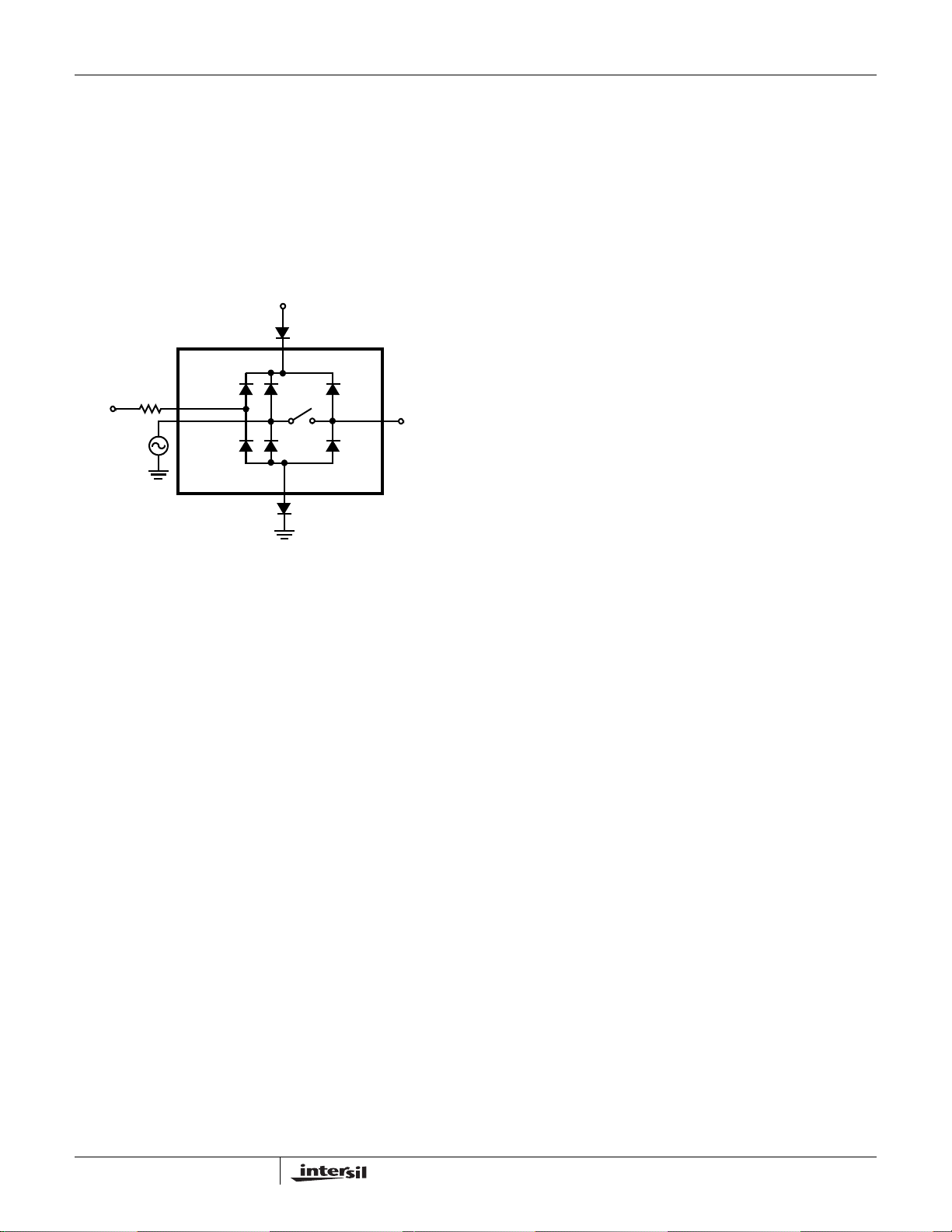
Supply Sequencing and Overvoltage Protection
With any CMOS device, proper power supply sequencing is
required to protect the device from excessive input currents
which might permanently damage the IC. All I/O pins contain
ESD protection diodes from the pin to V+ and to GND (see
Figure 8). To prevent forward biasing these diodes, V+ must
be applied before any input signals, and the input signal
voltages must remain between V+ and GND. If these
conditions cannot be guaranteed, then one of the following
two protection methods should be employed.
Logic inputs can easily be protected by adding a 1kΩ
resistor in series with the input (see Figure 8). The resistor
limits the input current below the threshold that produces
permanent damage, and the sub-microamp input current
produces an insignificant voltage drop during normal
operation.
6
FN6105.0
November 30, 2004
ISL84762
This method is not acceptable for the signal path inputs.
Adding a series resistor to the switch input defeats the
purpose of using a low R
switch, so two small signal
ON
diodes can be added in series with the supply pins to provide
overvoltage protection for all pins (see Figure 8). These
additional diodes limit the analog signal from 1V below V+ to
1V above GND. The low leakage current performance is
unaffected by this approach, but the switch signal range is
reduced and the resistance may increase, especially at low
supply voltages.
OPTIONAL PROTECTION
DIODE
OPTIONAL
PROTECTION
RESISTOR
IN
X
V
NO or NC
FIGURE 8. OVERVOLTAGE PROTECTION
V+
GND
OPTIONAL PROTECTION
DIODE
V
COM
Power-Supply Considerations
The ISL84762 construction is typical of most single supply
CMOS analog switches, in that they have two supply pins:
V+ and GND. V+ and GND drive the internal CMOS
switches and set their analog voltage limits. Unlike switches
with a 4V maximum supply voltage, the ISL84762 4.8V
maximum supply voltage provides plenty of room for the
10% tolerance of 3.6V supplies, as well as room for
overshoot and noise spikes.
The minimum recommended supply voltage is 1.65V but the
part will operate with a supply below 1.5V. It is important to
note that the input signal range, switching times, and onresistance degrade at lower supply voltages. Refer to the
electrical specification tables and Typical Performance
curves for details.
V+ and GND also power the internal logic and level shiftiers.
The level shiftiers convert the input logic levels to switched
V+ and GND signals to drive the analog switch gate
terminals.
This family of switches cannot be operated with bipolar
supplies, because the input switching point becomes
negative in this configuration.
Logic-Level Thresholds
This switch family is 1.8V CMOS compatible (0.5V and 1.4V)
over a supply range of 2.0V to 3.6V (see Figure 15). At 3.6V
the V
level is about 1.27V. This is still below the 1.8V
IH
CMOS guaranteed high output minimum level of 1.4V, but
noise margin is reduced.
The digital input stages draw supply current whenever the
digital input voltage is not at one of the supply rails. Driving
the digital input signals from GND to V+ with a fast transition
time minimizes power dissipation.
High-Frequency Performance
In 50Ω systems, the signal response is reasonably flat even
past 30MHz with a -3dB bandwidth of 120MHz (see Figure
16). The frequency response is very consistent over a wide
V+ range, and for varying analog signal levels.
An OFF switch acts like a capacitor and passes higher
frequencies with less attenuation, resulting in signal
feedthrough from a switch’s input to its output. Off Isolation is
the resistance to this feedthrough, while Crosstalk indicates
the amount of feedthrough from one switch to another.
Figure 17 details the high Off Isolation and Crosstalk
rejection provided by this part. At 100kHz, Off Isolation is
about 68dB in 50Ω systems, decreasing approximately 20dB
per decade as frequency increases. Higher load
impedances decrease Off Isolation and Crosstalk rejection
due to the voltage divider action of the switch OFF
impedance and the load impedance.
Leakage Considerations
Reverse ESD protection diodes are internally connected
between each analog-signal pin and both V+ and GND. One of
these diodes conducts if any analog signal exceeds V+ or
GND.
Virtually all the analog leakage current comes from the ESD
diodes to V+ or GND. Although the ESD diodes on a given
signal pin are identical and therefore fairly well balanced,
they are reverse biased differently. Each is biased by either
V+ or GND and the analog signal. This means their leakages
will vary as the signal varies. The difference in the two diode
leakages to the V+ and GND pins constitutes the analogsignal-path leakage current. All analog leakage current flows
between each pin and one of the supply terminals, not to the
other switch terminal. This is why both sides of a given
switch can show leakage currents of the same or opposite
polarity. There is no connection between the analog signal
paths and V+ or GND.
7
FN6105.0
November 30, 2004

ISL84762
Typical Performance Curves T
0.7
0.6
0.5
(Ω)
0.4
ON
R
0.3
0.2
0.1
V+ = 1.8V
V+ = 2.7V
V+ = 3V
01234
V
(V)
COM
V+ = 3.6V
= 25°C, Unless Otherwise Specified
A
I
= 100mA
COM
FIGURE 9. ON RESISTANCE vs SUPPLY VOLTAGE vs
SWITCH VOLTAGE
0.65
0.6
0.55
85°C
V+ = 1.8V
I
COM
= 100mA
0.44
0.42
0.4
0.38
(Ω)
ON
R
0.36
0.34
0.32
0.3
00.511.522.53
85°C
25°C
-40°C
V
COM
(V)
I
COM
V+ = 2.7V
= 100mA
FIGURE 10. ON RESISTANCE vs SWITCH VOLTAGE
100
75
V+ = 3V
50
(Ω)
0.5
ON
R
0.45
25°C
COM
-40°C
(V)
0.4
0.35
0 0.5 1 1.5 2
V
25
Q (pC)
0
-25
-50
00.511.522.53
V+ = 1.8V
V
COM
(V)
FIGURE 11. ON RESISTANCE vs SWITCH VOLTAGE FIGURE 12. CHARGE INJECTION vs SWITCH VOLTAGE
60
50
40
(ns)
ON
t
30
25°C
20
10
11.522.533.544.5
85°C
-40°C
V+ (V)
14
13
12
11
10
9
(ns)
8
OFF
t
7
6
5
4
3
1
85°C
-40°C
25°C
1.5 2 2.5 3 3.5 4 4.5
V+ (V)
FIGURE 13. TURN - ON TIME vs SUPPLY VOLTAGE FIGURE 14. TURN - OFF TIME vs SUPPLY VOLTAGE
8
FN6105.0
November 30, 2004

V
AND
V
(V)
ISL84762
Typical Performance Curves T
1.5
1.4
1.3
1.2
1.1
1
INL
0.9
0.8
0.7
INH
0.6
0.5
0.4
0.3
11.522.533.544.5
V
INH
V
INL
V+ (V)
= 25°C, Unless Otherwise Specified (Continued)
A
V+ = 3V
0
GAIN
-20
PHASE
NORMALIZED GAIN (dB)
RL = 50Ω
VIN = 0.2V
1 10 100 600
P-P
to 2V
P-P
FREQUENCY (MHz)
FIGURE 15. DIGITAL SWITCHING POINT vs SUPPLY VOLTAGE FIGURE 16. FREQUENCY RESPONSE
-10
V+ = 3V
-20
-30
-40
-50
10
20
30
40
50
Die Characteristics
SUBSTRATE POTENTIAL (POWERED UP):
GND (QFN Paddle Connection: Tie to GND or Float)
TRANSISTOR COUNT:
114
0
20
40
60
80
100
PHASE (DEGREES)
-60
-70
CROSSTALK (dB)
-80
-90
-100
-110
1k 100k 1M 100M 500M10k 10M
ISOLATION
CROSSTALK
FREQUENCY (Hz)
60
70
80
90
100
110
PROCESS:
Submicron CMOS
OFF ISOLATION (dB)
FIGURE 17. CROSSTALK AND OFF ISOLATION
9
FN6105.0
November 30, 2004

ISL84762
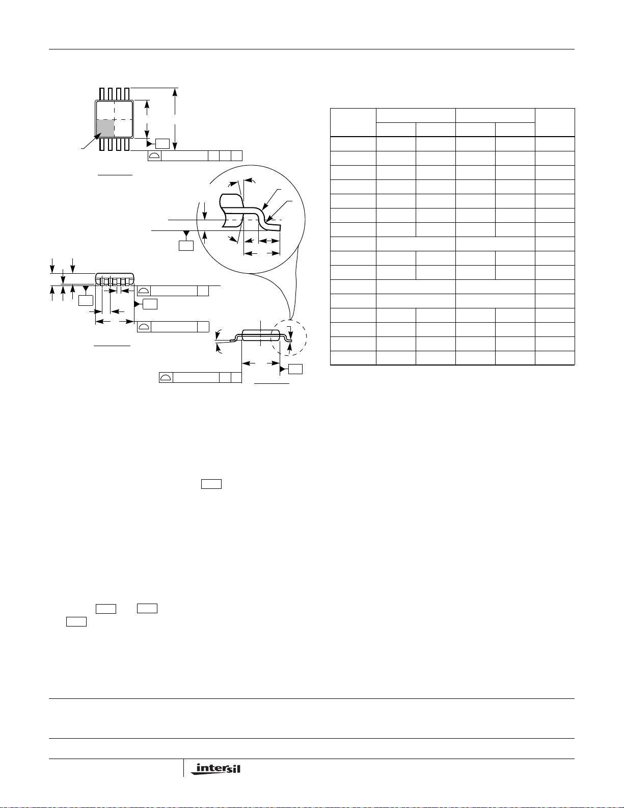
Thin Dual Flat No-Lead Plastic Package (TDFN)
(DATUM B)
6
INDEX
AREA
(DATUM A)
NX (b)
5
SECTION "C-C"
A
6
INDEX
AREA
SEATING
PLANE
NX L
8
C
12
N
BOTTOM VIEW
D
TOP VIEW
SIDE VIEW
D2
N-1
e
(Nd-1)Xe
REF.
(A1)
D2/2
CC
e
2X
A3
NX b
5
C
L
87
E2/2
0.10
ABC0.15
2X
0.15
E
//
A
NX k
E2
M
TERMINAL TIP
0.10
0.08
L1
CB
BAC
L10.3x3A
10 LEAD THIN DUAL FLAT NO-LEAD PLASTIC PACKAGE
MILLIMETERS
SYMBOL
A 0.70 0.75 0.80 -
A1 - - 0.05 -
A3 0.20 REF -
b 0.20 0.25 0.30 5,8
D 3.00 BSC -
D2 2.20 2.30 2.40 7,8
E 3.00 BSC -
C
C
E2 1.40 1.50 1.60 7,8
e 0.50 BSC -
k0.25 - - -
L 0.20 0.30 0.40 8
L1 - - 0.15 1
N102
Nd 5 3
NOTES:
1. Dimensioning and tolerancing conform to ASME Y14.5-1994.
2. N is the number of terminals.
3. Nd refers to the number of terminals on D.
4. All dimensions are in millimeters. Angles are in degrees.
5. Dimension b applies to the metallized terminal and is measured
between 0.15mm and 0.30mm from the terminal tip.
6. The configuration of the pin #1 identifier is optional, but must be
located within the zone indicated. The pin #1 identifier may be
either a mold or mark feature.
7. Dimensions D2 and E2 are for the exposed pads which provide
improved electrical and thermal performance.
8. Nominal dimensions are provided to assist with PCB Land
Pattern Design efforts, see Intersil Technical Brief TB389.
L
9
9. Depending on the method of lead termination at the edge of the
package, a maximum 0.15mm pull back (L1) maybe present. L
minus L1 to be equal to or greater than 0.3mm.
10. COMPLIANT TO JEDEC MO-229-WEED-3 except for
dimensions E2 & D2.
NOTESMIN NOMINAL MAX
Rev. 1 6/04
FOR ODD TERMINAL/SIDE
10
FN6105.0
November 30, 2004
ISL84762
Mini Small Outline Plastic Packages (MSOP)
N
EE1
INDEX
AREA
AA1A2
-H-
SIDE VIEW
12
TOP VIEW
b
e
D
NOTES:
1. These package dimensions are within allowable dimensions of
JEDEC MO-187BA.
2. Dimensioning and tolerancing per ANSI Y14.5M-1994.
3. Dimension “D” does not include mold flash, protrusions or gate
burrs and are measured at Datum Plane. Mold flash, protrusion
and gate burrs shall not exceed 0.15mm (0.006 inch) per side.
4. Dimension “E1” does not include interlead flash or protrusions
and are measured at Datum Plane. Interlead flash and
protrusions shall not exceed 0.15mm (0.006 inch) per side.
5. Formed leads shall be planar with respect to one another within
0.10mm (.004) at seating Plane.
6. “L” is the length of terminal for soldering to a substrate.
7. “N” is the number of terminal positions.
8. Terminal numbers are shown for reference only.
9. Dimension “b” does not include dambar protrusion. Allowable
dambar protrusion shall be 0.08mm (0.003 inch) total in excess
of “b” dimension at maximum material condition. Minimum space
between protrusion and adjacent lead is 0.07mm (0.0027 inch).
- H -
-A -
.
10. Datums and to be determined at Datum plane
11. Controlling dimension: MILLIMETER. Converted inch dimensions are for reference only
-B-
0.20 (0.008) A
GAUGE
PLANE
SEATING
PLANE
0.10 (0.004) C
-A-
0.20 (0.008) C
- B -
0.25
(0.010)
-C-
SEATING
PLANE
a
0.20 (0.008) C
- H -
B
4X θ
C
D
4X θ
L1
C
C
L
E
1
END VIEW
R1
R
L
-B-
M10.118 (JEDEC MO-187BA)
10 LEAD MINI SMALL OUTLINE PLASTIC PACKAGE
INCHES MILLIMETERS
SYMBOL
A 0.037 0.043 0.94 1.10 A1 0.002 0.006 0.05 0.15 A2 0.030 0.037 0.75 0.95 -
b 0.007 0.011 0.18 0.27 9
c 0.004 0.008 0.09 0.20 -
D 0.116 0.120 2.95 3.05 3
E1 0.116 0.120 2.95 3.05 4
e 0.020 BSC 0.50 BSC -
E 0.187 0.199 4.75 5.05 -
L 0.016 0.028 0.40 0.70 6
L1 0.037 REF 0.95 REF -
N10 107
R 0.003 - 0.07 - R1 0.003 - 0.07 - -
o
θ
α
5
o
0
15
o
o
6
o
5
o
0
15
o
o
6
Rev. 0 12/02
NOTESMIN MAX MIN MAX
-
-
All Intersil U.S. products are manufactured, assembled and tested utilizing ISO9000 quality systems.
Intersil Corporation’s quality certifications can be viewed at www.intersil.com/design/quality
Intersil products are sold by description only. Intersil Corporation reserves the right to make changes in circuit design, software and/or specifications at any time without
notice. Accordingly, the reader is cautioned to verify that data sheets are current before placing orders. Information furnished by Intersil is believed to be accurate and
reliable. However, no responsibility is assumed by Intersil or its subsidiaries for its use; nor for any infringements of patents or other rights of third parties which may result
from its use. No license is granted by implication or otherwise under any patent or patent rights of Intersil or its subsidiaries.
For information regarding Intersil Corporation and its products, see www.intersil.com
11
FN6105.0
November 30, 2004
 Loading...