

®
ISL84516, ISL84517
Data Sheet May 19, 2005
Low-Voltage, Dual Supply, SPST, Analog
Switches
The Intersil ISL84516 and ISL84517 devices are preci sion,
analog switches designed to o perate from ±1.5V to ±6V
supplies. Targeted applications include battery powered
equipment that benefit from the devices’ low po w er
consumption (350mW), low leakage currents, and fast
switching speeds. Additionally, excellent R
flatness
ON
maintains signal fidelity over the whole in put r ange , while
micro packaging alleviate s board space limita ti ons .
The ISL8451X are single-pole/single-throw (SPST) switches ,
with the ISL84516 being normally open (NO), and the
ISL84517 being normally closed (NC).
Table 1 summarizes the performance of this family. For
higher performance, pin compatible versions, see the
ISL43112, ISL43113 data sheet. For single supply versions,
see the ISL84514, ISL84515 data sheet.
TABLE 1. FEATURES AT A GLANCE
ISL84516 ISL84517
Number of Switches 1 1
Configuration NO NC
±5V R
ON
±5V t
ON/tOFF
Packages 8 Ld SOIC, 5 Ld SOT-23
13Ω 13Ω
40ns / 30ns 40ns / 30ns
Related Literature
• Technical Brief TB363 “Guidelines for Handling and
Processing Moisture Sensitive Surface Mount Devices
(SMDs)”
• Application Note AN557 “Recommended Test Procedures
for Analog Switches”
FN6030.4
Features
• Drop-in Replacements for MAX4516 and MAX4517 at
= ±5V
V
S
• Available in SOT-23 Packaging
• Dual Supply Operation . . . . . . . . . . . . . . . . . . . ±1.5V to ±6V
• ON Resistance (R
Flatness . . . . . . . . . . . . . . . . . . . . . . . . . . . . . . . . . . . 3Ω
•R
ON
Max). . . . . . . . . . . . . . . . . . . . . 20Ω
ON
• Charge Injection . . . . . . . . . . . . . . . . . . . . . . . . . 20pC (Max)
• Low Leakage Current (Max at 85oC) . 20nA (Off Leakage)
. . . . . . . . . . . . . . . . . . . . . . . . . . . . . . 40nA (On Leakage)
• Fast Switching Action
(Max) . . . . . . . . . . . . . . . . . . . . . . . . . . . . . . 100ns
-t
ON
(Max) . . . . . . . . . . . . . . . . . . . . . . . . . . . . . . 75ns
-t
OFF
• Minimum 2000V ESD Protection per Method 3015.7
• CMOS Logic Compatible
• Pb-Free Available (RoHS Compliant)
Applications
• Battery Powered, Handheld, and Portable Equipment
• Communications Systems
-Radios
- Telecom Infr ustructure
• Medical Equipment
- Ultrasound, MRI, CAT/PET SCAN
- Electrocardiograph, Blood Analyzer
• Test Equipment
- Logic and Spectrum Analyzers
- Portable Meters, DVM, DMM
• Audio and Video Switching
• General Purpose Circuits
- Low Voltage DACs and ADCs
- Sample and Hold Circuits
- Digital Filters
- Operational Amplifier Gain Switching Networks
- High Frequency Analog Switching
- High Speed Multiplexing
- Integrator Reset Circuits
1
CAUTION: These devices are sensitive to electrostatic discharge; follow proper IC Handling Procedures.
1-888-INTERSIL or 321-724-7143
| Intersil (and design) is a registered trademark of Intersil Americas Inc.
Copyright © Intersil Americas Inc. 2003-2005. All Rights Reserved
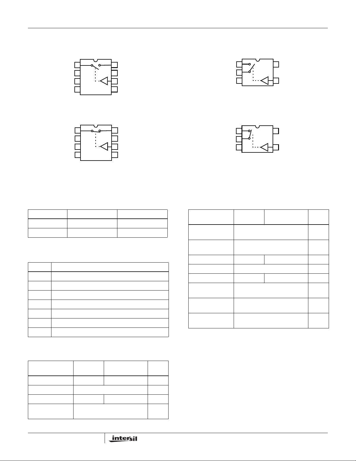
Pinouts (Note 1)
COM
N.C.
N.C.
V+
ISL84516 (SOIC)
TOP VIEW
1
2
3
4
ISL84516, ISL84517
ISL84516 (SOT-23)
TOP VIEW
V+
1
8
NO
7
V-
6
IN
5
N.C.
COM
NO
2
3
V-
5
4
IN
ISL84517 (SOIC)
TOP VIEW
COM
N.C.
N.C.
V+
1
2
3
4
8
NC
7
V-
6
IN
5
N.C.
NOTE:
1. Switches Shown for Logic “0” Input.
Truth Table
LOGIC ISL84516 ISL84517
0OFF ON
1ON OFF
NOTE: Logic “0” ≤ 1.5V; Logic “1” ≥ 3.5V at V
= ±5V
S
Pin Descriptions
PIN FUNCTION
V+ System Positive Power Supply Input (+1.5V to +6V)
V- System Negative Power Supply Input (-1.5V to -6V)
IN CMOS Compatible Digital Control Input
COM Analog Switch Common Pin
NO Analog Switch Normally Open Pin
NC Analog Switch Normally Closed Pin
N.C. No Internal Connection
Ordering Information
PART NO.
(BRAND)
ISL84516IB -40 to 85 8 Ld SOIC M8.15
ISL84516IB-T 8 Ld SOIC Tape and Reel M8.15
ISL84516IBZ (Note) -40 to 85 8 Ld SOIC (Pb-free) M8.15
ISL84516IBZ-T
(Note)
TEMP.
RANGE (
o
C) PACKAGE
8 Ld SOIC Tape and Reel
(Pb-free
PKG.
DWG. #
M8.15
ISL84517 (SOT-23)
TOP VIEW
V+
COM
NC
1
2
3
V-
5
4
IN
Ordering Information (Continued)
PART NO.
(BRAND)
ISL84516IH-T
(516I)
ISL84516IHZ-T
(516I) (Note)
ISL84517IB -40 to 85 8 Ld SOIC M8.15
ISL84517IB-T 8 Ld SOIC, Tape and Reel M8.15
ISL84517IBZ (Note) -40 to 85 8 Ld SOIC (Pb-free) M8.15
ISL84517IBZ-T
(Note)
ISL84517IH-T
(517I)
ISL84517IHZ-T
(517I) (Note)
NOTE: Intersil Pb-free products employ special Pb-free material sets;
molding compounds/die attach materials and 100% matte tin plate
termination finish, which are RoHS compliant and compatible with
both SnPb and Pb-free soldering operations. Intersil Pb-free products
are MSL classified at Pb-free peak reflow temperatures that meet or
exceed the Pb-free requirements of IPC/JEDEC J STD-020.
TEMP.
RANGE (
o
C) PACKAGE
PKG.
DWG. #
5 Ld SOT-23, Tape and Reel P5.064
5 Ld SOT-23, Tape and Reel
P5.064
(Pb-free)
8 Ld SOIC, Tape and Reel
M8.15
(Pb-free)
5 Ld SOT-23, Tape and Reel P5.064
5 Ld SOT-23, Tape and Reel
P5.064
(Pb-free)
2
ISL84516, ISL84517
Absolute Maximum Ratings Thermal Information
V+ to V- . . . . . . . . . . . . . . . . . . . . . . . . . . . . . . . . . . . . . -0.3 to 15V
Input Voltages
IN (Note 2). . . . . . . . . . . . . . . . . . . . . ((V-) - 0.3V) to ((V+) + 0.3V)
NO, NC (Note 2) . . . . . . . . . . . . . . . . ((V-) - 0.3V) to ((V+) + 0.3V)
Output Voltages
COM (Note 2) . . . . . . . . . . . . . . . . . . ((V-) - 0.3V) to ((V+) + 0.3V)
Continuous Current (Any Terminal) . . . . . . . . . . . . . . . . . . . . . 20mA
Peak Current NO, NC, or COM
(Pulsed 1ms, 10% Duty Cycle, Max) . . . . . . . . . . . . . . . . . . 30mA
ESD Rating (Per MIL-STD-883 Method 3015). . . . . . . . . . . . . >2kV
Operating Conditions
Temperature Range
ISL8451XIX . . . . . . . . . . . . . . . . . . . . . . . . . . . . . . . . -40
CAUTION: Stresses above those listed in “Absolute Maximum Ratings” may cause permanent damage to the device. This is a stress only rating and operation of the
device at these or any other conditions above those indicated in the operational sections of this specification is not implied.
NOTES:
2. Signals on NO, NC, COM, or IN exceeding V+ or V- are clamped by internal diodes. Limit forward diode current to maximum current ratings.
is measured with the component mounted on a low effective thermal conductivity test board in free air. See Tech Brief TB379 for details.
3. θ
JA
o
C to 85oC
Thermal Resistance (Typical, Note 3) θ
(oC/W)
JA
5 Ld SOT-23 Package . . . . . . . . . . . . . . . . . . . . . . . 225
8 Ld SOIC Package . . . . . . . . . . . . . . . . . . . . . . . . . 170
Maximum Junction Temperature (Plastic Package). . . . . . . . 150
Moisture Sensitivity (See Technical Brief TB363)
All Packages. . . . . . . . . . . . . . . . . . . . . . . . . . . . . . . . . . . . Level 1
Maximum Storage T emperature Range. . . . . . . . . . . . -65
o
C to 150oC
Maximum Lead Temperature (Soldering 10s) . . . . . . . . . . . . 300
(Lead Tips Only)
o
o
C
C
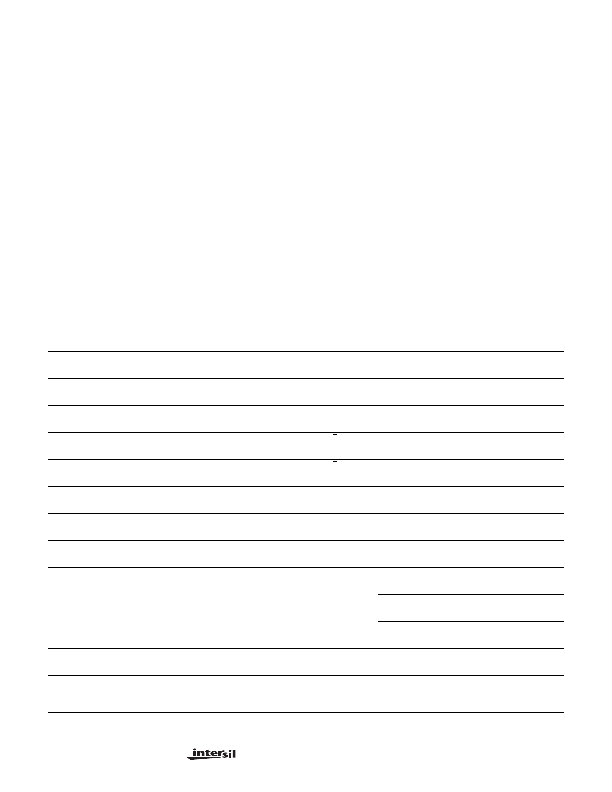
Electrical Specifications - ±5V Supply Test Conditions: V
Unless Otherwise Specified
PARAMETER TEST CONDITIONS
ANALOG SWITCH CHARACTERISTICS
Analog Signal Range, V
ON Resistance, R
R
Flatness, R
ON
NO or NC OFF Leakage Current,
I
NO(OFF)
or I
NC(OFF)
COM OFF Leakage Current,
I
COM(OFF)
COM ON Leakage Current,
I
COM(ON)
DIGITAL INPUT CHARACTERISTICS
Input Voltage High, V
Input Voltage Low, V
Input Current, I
INH
DYNAMIC CHARACTERISTICS
Turn-ON Time, t
Turn-OFF Time, t
Charge Injection, Q C
OFF Isolation R
NO or NC OFF Capacitance, C
COM OFF Capacitance,
C
COM(OFF)
COM ON Capacitance, C
ON
FLAT(ON)
INH
INL
, I
INL
ON
OFF
ANALOG
COM(ON)
VS = ±5V, I
(See Figure 4)
VS = ±5V, I
VS = ±5.5V, V
(Note 6)
VS = ±5.5V, V
(Note 6)
VS = ±5.5V, V
= 1.0mA, V
COM
= 1.0mA, V
COM
= ±4.5V, VNO or VNC = +4.5V
COM
= ±4.5V, VNO or VNC = +4.5V
COM
= VNO or VNC = ±4.5V (Note 6) 25 -2 0.01 2 nA
COM
COM
COM
VS = ±5.5V, VIN = 0V or V+ Full -0.5 - 0.5 µA
VNO or VNC = 3V, RL = 300Ω, CL = 35pF,
V
= 0 to V+ (See Figure 1)
IN
VNO or VNC = 3V, RL = 300Ω, CL = 35pF,
V
= 0 to V+ (See Figure 1)
IN
= 1.0nF, VG = 0V, RG = 0Ω (See Figure 2) 25 - 10 20 pC
L
= 50Ω, CL = 15pF, f = 100kHz (See Figure 3) 25 - >86 - dB
L
f = 1MHz, VNO or VNC = V
OFF
f = 1MHz, VNO or VNC = V
f = 1MHz, VNO or VNC = V
= 0V (See Figure 5) 25 - 9 - pF
COM
= 0V (See Figure 5) 25 - 9 - pF
COM
= 0V (See Figure 5) 25 - 22 - pF
COM
= ±4.5V to ±5.5V, V
SUPPLY
TEMP
o
(
C)
= 3.5V, V
INH
(NOTE 5)
= 1.5V (Note 4),
INL
MIN TYP
(NOTE 5)
MAX UNITS
Full V- - V+ V
= 3V
25 - 13 20 Ω
Full - - 25 Ω
= -3V, 0V, 3V 25 - 3 4 Ω
Full - 4 6 Ω
25 -1 0.01 1 nA
Full -20 - 20 nA
25 -1 0.01 1 nA
Full -20 - 20 nA
Full -40 - 40 nA
Full (V+) - 1.5 - V+ V
Full V- - (V+) - 3.5 V
25 - 40 100 ns
Full - - 150 ns
25 - 30 75 ns
Full - - 125 ns
3

ISL84516, ISL84517
Electrical Specifications - ±5V Supply Test Conditions: V
= ±4.5V to ±5.5V, V
SUPPLY
= 3.5V, V
INH
= 1.5V (Note 4),
INL
Unless Otherwise Specified (Continued)
PARAMETER TEST CONDITIONS
TEMP
o
C)
(
(NOTE 5)
MIN TYP
(NOTE 5)
MAX UNITS
POWER SUPPLY CHARACTERISTICS
Power Supply Range Full ±1.5 - ±6V
Positive Supply Current, I+ V
= ±5.5V, VIN = 0V or V+, Switch On or Off 25 - 40 125 µA
S
Full - - 200 µA
Negative Supply Current, I- V
= ±5.5V, VIN = 0V or V+, Switch On or Off 25 -125 30 - µA
S
Full -200 - - µA
NOTES:
4. V
= Input voltage to perform proper function.
IN
5. The algebraic convention, whereby the most negative value is a minimum and the most positive a maximum, is used in this data sheet.
o
6. Leakage parameter is 100% tested at high temp, and guaranteed by correlation at 25
C.
Test Circuits and Waveforms
V+
C
V
OUT
COM
C
RL
300Ω
C
V-
L
35pF
LOGIC
INPUT
SWITCH
INPUT
SWITCH
OUTPUT
V+
0V
0V
t
ON
50%
90%
t
OFF
V
OUT
tr < 20ns
< 20ns
t
f
90%
SWITCH
LOGIC
INPUT
NO or NC
INPUT
IN
FIGURE 1A. MEASUREMENT POINTS
Logic input waveform is inverted for switches that have the opposite
logic sense.
FIGURE 1. SWITCHING TIMES
SWITCH
OUTPUT
V
OUT
LOGIC
INPUT
ON
Q = ∆V
OUT
∆V
x C
OUT
ON
OFF
L
FIGURE 2A. MEASUREMENT POINTS
FIGURE 2. CHARGE INJECTION
FIGURE 1B. TEST CIRCUIT
C
includes fixture and stray capacitance.
L
V
=
V
OUT
R
G
V
G
V+
NO or NC
C
V-
(NO or NC)
C
FIGURE 2B. TEST CIRCUIT
------------------------------
RLR
COM
IN
LOGIC
INPUT
+
R
L
ON()
V
OUT
C
L
4

Test Circuits and Waveforms (Continued)
ISL84516, ISL84517
SIGNAL
GENERATOR
ANALYZER
FIGURE 3. OFF ISOLATION TEST CIRCUIT
V+
C
RON = V1/1mA
NO or NC
V
COM
V- or V+
IN
COM
R
L
C
V-
NO or NC
1mA
FIGURE 4. RON TEST CIRCUIT
V+
V
COM
1
NO or NC
V+
C
or V
V
INL
IN
C
V-
INH
IMPEDANCE
ANALYZER
FIGURE 5. CAPACITANCE TEST CIRCUIT
Detailed Description
The ISL84516 and ISL84517 analog switches offer precise
switching capability from ±1.5V to ±6V supplies with low onresistance (13Ω) and high speed operation (t
t
= 30ns). The devices are especially well suited to
OFF
portable battery powered equipment thanks to the low
operating supply voltage (±1.5V), low power consumption
(350µW), low leakage currents (2nA max), and the tin y
SOT-23 packag ing. High fre quency applications also benefit
from the wide bandwidth, and the very high off isolation.
Supply Sequencing And Overvoltage Protection
With any CMOS device, proper power supply sequencing is
required to protect the device from excessiv e input currents
which might permanently damage the IC. All I/O pins contain
ESD protection diodes from the pin to V+ and to V- (see
Figure 6). To prevent forward biasing these diodes, V+ and
ON
= 40ns,
V- or V+
IN
COM
V-
V - must be applied before any input signals, and input signal
voltages must remain between V+ and V -. If these conditions
cannot be guaranteed, then one of the following two
protection methods should be employed.
Logic inputs can easily be protected by adding a 1kΩ
resistor in series with the input (see Figure 6). The resistor
limits the input current below the threshold that produces
permanent damage, and the sub-microamp input current
produces an insignificant voltage drop during normal
operation.
Adding a series resistor to the switch input defeats the
purpose of using a low R
switch, so two small signal
ON
diodes can be added in series with the supply pins to provide
overvoltage protection for all pins (see Figure 6). These
additional diodes limit the analog signal from 1V below V+ to
1V above V-. The low leakage current performance is
5

ISL84516, ISL84517
unaffected by this approach, but the switch resistance may
increase, especially at low supply voltage.
OPTIONAL PROTECTION
DIODE
OPTIONAL
PROTECTION
RESISTOR
IN
V
NO or NC
FIGURE 6. OVERVOLTAGE PROTECTION
V+
V
V-
OPTIONAL PROTECTION
DIODE
COM
Power-Supply Considerations
The ISL8451X construction is typical of most CMOS analog
switches, except that there are only two supply pins: V+ and
V-. The power supplies need not be symmetrical for useful
operation. As long as the total supply voltage (V+ to V-,
including supply tolerances, overshoot, and noise spikes) is
less than the15V maximum supply rating, and the digital
input switching point remains reasonable (see “Logic-Level
Thresholds” section), the ISL84516, ISL84517 function well.
The 15V maximum supply rating provides the designer of
12V systems much greater flexibility than switches with a
13V maximum supply voltage.
The minimum recommended supply voltage is ±1.5V. It is
important to note that the input signal range, switching times,
and on-resistance degrade at lower supply voltages, and the
digital input V
“Typical Performance” curves for details.
V+ and V- power the internal CMOS switches and set their
analog voltage limits. These supplies also power the internal
logic and level shifters. The level shifters convert the input
logic levels to switched V+ and V- signals to drive the analog
switch gate terminals.
This family of switches is not recommended for single supply
applications. For single supply, similar performance, pin
compatible, TTL compatible versions of these switches, see
the ISL84514, ISL84515 data sheet.
becomes negative at VS ≤ ±2V. Refer to the
IL
Logic-Level Thresholds
Due to the lack of a GND pin, the switching point of the
digital input is referenced predominantly to V+. The digital
input is CMOS compatible at ±5V supplies, and is TTL
compatible for ±3.3V supplies. F or other supply
combinations refer to Figure 11.
The switching point has a very low temperature sensitivity,
and changes by only 100mV from 85
o
C to -40oC, regardless
of supply voltage.
High-Frequency Performance
In 50Ω systems, signal response is reasonably flat to
30MHz, with a -3dB bandwidth of nearly 400MHz (see
Figure 13). Figure 13 also illustrates that the frequency
response is very consistent over a wide V+ range, and for
varying analog signal levels.
An OFF switch acts like a capacitor and passes higher
frequencies with less attenuation, resulting in signal
feedthrough from a switch’s input to its output. OFF Isolation
is the resistance to this feedthrough. Figure 14 details the
high OFF Isolation provided by this family. At 10MHz, OFF
Isolation is about 50dB in 50Ω systems, decreasing
approximately 20dB per decade as frequency increases.
Higher load impedances decrease OFF Isolation due to the
voltage divider action of the switch OFF Impedance and the
load impedance.
Leakage Considerations
Reverse ESD protection diodes are internally connected
between each analog-signal pin and both V+ and V-. One of
these diodes conducts if any analog signal exceeds V+ or
V-.
Virtually all the analog leakage current comes from the ESD
diodes to V+ or V-. Although the ESD diodes on a given
signal pin are identical and therefore fairly well balanced,
they are reverse biased differently. Each is biased by either
V+ or V- and the analog signal. This means their leakages
will vary as the signal varies. The difference in the two diode
leakages to the V+ and V- pins constitutes the analog-signalpath leakage current. All analog leakage current flows
between each pin and one of the supply terminals, not to the
other switch terminal. This is why both sides of a given
switch can show leakage currents of the same or opposite
polarity . There is no connection between the analog-signal
paths and V+ or V-.
6

ISL84516, ISL84517
Typical Performance Curves T
150
-40oC
125
100
75
(Ω)
ON
R
50
25
0
123456
25oC
85oC
-40oC
VS (±V)
= 25oC, VIH = V+, VIL = 0V, Unless Otherwise Specified
A
V
= (V+) -1V
COM
I
= 1mA
COM
FIGURE 7. ON RESISTANCE vs SUPPLY VOLTAGE
120
100
100
90
80
(ns)
70
ON
t
60
50
40
30
12345 6
85oC
25oC
-40oC
VS (±V)
V
COM
= (V+) -1V
V
= 0 to V+
IN
RL = 300Ω
FIGURE 9. TURN - ON TIME vs SUPPLY VOLTAGE
50
I
= 1mA
COM
45
40
35
30
25
20
30
85oC
25
(Ω)
ON
R
25oC
20
-40oC
15
10
30
25
20
15
10
5
-5 -2 0 2 4 5-4 -3 -1 1 3
85oC
-40oC
25oC
V
COM
(V)
85oC
25oC
-40oC
VS = ±1.5V
VS = ±3.3V
VS = ±5V
FIGURE 8. ON RESISTANCE vs SWITCH VOLTAGE
80
70
85oC
60
50
(ns)
40
OFF
t
30
20
10
12345 6
25oC
-40oC
VS (±V)
V
COM
= (V+) -1V
V
= 0 to V+
IN
RL = 300Ω
FIGURE 10. TURN - OFF TIME vs SUPPLY VOLTAGE
3.5
-40oC to 85oC
3
2.5
2
(V)
INL
1.5
V
INH
1
AND V
INH
V
0.5
0
V
INL
-0.5
123456
(±V)
V
S
FIGURE 11. DIGITAL SWITCHING POINT vs SUPPLY VOLTAGE
7
40
30
20
10
0
V
COM
VS = ±1.5V
(V)
Q (pC)
-10
-20
-30
-40
-5 -4 -2 0 2 4 5
VS = ±3.3V
-3 -1 1 3
VS = ±5V
FIGURE 12. CHARGE INJECTION vs SWITCH VOLTAGE

ISL84516, ISL84517
Typical Performance Curves T
VS = ±1.5V to ±5.5V
0
GAIN
-3
-6
PHASE
NORMALIZED GAIN (dB)
RL = 50Ω
VIN = 0.2V
= 0.2V
V
IN
= 0.2V
V
IN
1 10 100 600
P-P
P-P
P-P
to 2V
to 4V
to 5V
(VS = ±1.5V)
P-P
(VS = ±3.3V)
P-P
(VS = ±5.5V)
P-P
FREQUENCY (MHz)
= 25oC, VIH = V+, VIL = 0V, Unless Otherwise Specified (Continued)
A
FIGURE 13. FREQUENCY RESPONSE FIGURE 14. OFF ISOLATION
25
20
0
45
90
135
180
PHASE (DEGREES)
10
VS = ±1.5V to ±5.5V
20
RL = 50Ω
30
40
50
60
70
OFF ISOLATION (dB)
80
90
100
110
1k 100k 1M 100M 500M10k 10M
FREQUENCY (Hz)
15
(µA)
CC
10
I
5
0
123456
FIGURE 15. SUPPLY CURRENT vs SUPPLY VOLTAGE
Die Characteristics
SUBSTRATE POTENTIAL (POWERED UP):
V-
TRANSISTOR COUNT:
ISL84516: 55
ISL84517: 55
PROCESS:
Si Gate CMOS
-40oC
25oC
85oC
VS (±V)
8

ISL84516, ISL84517
Small Outline Plastic Packages (SOIC)
N
INDEX
AREA
123
SEA TING PLANE
-AD
e
B
0.25(0.010) C AM BS
E
-B-
A
-C-
M
0.25(0.010) BM M
H
α
µ
A1
0.10(0.004)
L
h x 45
o
C
NOTES:
1. Symbols are defined in the “MO Series Symbol List” in Section 2.2 of
Publication Number 95.
2. Dimensioning and tolerancing per ANSI Y14.5M-1982.
3. Dimension “D” does not include mold flash, protrusions or gate burrs.
Mold flash, protrusion and gate burrs shall not exceed 0.15mm (0.006
inch) per side.
4. Dimension “E” does not include interlead flash or protrusions. Interlead flash and protrusions shall not exceed 0.25mm (0.010 inch) per
side.
5. The chamfer on the body is optional. If it is not present, a visual index
feature must be located within the crosshatched area.
6. “L” is the length of terminal for soldering to a substrate.
7. “N” is the number of terminal positions.
8. Terminal numbers are shown for reference only.
9. The lead width “B”, as measured 0.36mm (0.014 inch) or greater
above the seating plane, shall not exceed a maximum value of
0.61mm (0.024 inch).
10. Controlling dimension: MILLIMETER. Converted inch dimensions
are not necessarily exact.
M8.15 (JEDEC MS-012-AA ISSUE C)
8 LEAD NARROW BODY SMALL OUTLINE PLASTIC
PACKAGE
INCHES MILLIMETERS
SYMBOL
A 0.0532 0.0688 1.35 1.75 -
A1 0.0040 0.0098 0.10 0.25 -
B 0.013 0.020 0.33 0.51 9
C 0.0075 0.0098 0.19 0.25 D 0.1890 0.1968 4.80 5.00 3
E 0.1497 0.1574 3.80 4.00 4
e 0.050 BSC 1.27 BSC H 0.2284 0.2440 5.80 6.20 h 0.0099 0.019 6 0.25 0.50 5
L 0.016 0.050 0.40 1.27 6
N8 87
o
α
0
o
8
o
0
o
8
Rev. 0 12/93
NOTESMIN MAX MIN MAX
-
9

ISL84516, ISL84517
Small Outline Transistor Plastic Packages (SOT23-5)
E
A2
A
SEATING
PLANE
D
e1
123
e
C
L
0.20 (0.008) M
PLATING
4X θ1
C
4X θ1
C
L
WITH
C
c
BASE METAL
45
C
L
b
A1
0.10 (0.004) C
b
b1
R1
L
α
L1
C
L
SEATING
PLANE
R
-C-
VIEW C
α
c1
GAUGE PLANE
L2
E1
P5.064
5 LEAD SMALL OUTLINE TRANSISTOR PLASTIC PACKAGE
INCHES MILLIMETERS
SYMBOL
A 0.036 0.057 0.90 1.45 A1 0.000 0.0059 0.00 0.15 A2 0.036 0.051 0.90 1.30 -
b 0.012 0.020 0.30 0.50 -
b1 0.012 0.018 0.30 0.45
c 0.003 0.009 0.08 0.22 6
c1 0.003 0.008 0.08 0.20 6
C
D 0.111 0.118 2.80 3.00 3
E 0.103 0.118 2.60 3.00 E1 0.060 0.067 1.50 1.70 3
e 0.0374 Ref 0.95 Ref -
e1 0.0748 Ref 1.90 Ref -
L 0.014 0.022 0.35 0.55 4
L1 0.024 Ref. 0.60 Ref.
L2 0.010 Ref. 0.25 Ref.
N5 55
R 0.004 - 0.10 R1 0.004 0.010 0.10 0.25
o
α
0
o
8
o
0
NOTES:
1. Dimensioning and tolerance per ASME Y14.5M-1994.
2. Package conforms to EIAJ SC-74 and JEDEC MO178AA.
3. Dimensions D and E1 are exclusive of mold flash, protrusions,
or gate burrs.
4. Footlength L measured at reference to gauge plane.
5. “N” is the number of terminal positions.
6. These Dimensions apply to the flat section of the lead between
0.08mm and 0.15mm from the lead tip.
7. Controlling dimension: MILLIMETER. Converted inch dimensions are for reference only.
o
8
NOTESMIN MAX MIN MAX
-
Rev. 2 9/03
VIEW C
All Intersil U.S. products are manufactured, assembled and tested utilizing ISO9000 quality systems.
Intersil Corporation’s quality certifications can be viewed at www.intersil.com/design/quality
Intersil products are sold by description only. Intersil Corporation reserves the right to make changes in circuit design, software and/or specifications at any time without
notice. Accordingly, the reader is cautioned to verify that data sheets are current before placing orders. Information furnished by Intersil is believed to be accurate and
reliable. However, no responsibility is assumed by Intersil or its subsidiaries for its use; nor for any infringements of patents or other rights of third parties which may result
from its use. No license is granted by implication or otherwise under any patent or pat ent rights of In tersi l or its subs idiaries.
For information regarding Intersil Corporation and its products, see www.intersil.com
10
 Loading...