®
www.BDTIC.com/Intersil
ISL83386E
Data Sheet November 19, 2004
±15kV ESD Protected, +3V to +5.5V,
1 Microamp, 250kbps, RS-232
Transmitters/Receivers with Separate
Logic Supply
The ISL83386E contains 3.0V to 5.5V powered RS-232
transmitters/receivers which meet ElA/TIA-232 and
V.28/V.24 specifications, even at V
applications are PDAs, Palmtops , and cell phones where the
low operational, and even lower standb y, power consumption
is critical. Efficient on-chip charge pumps, coupled with a
manual powerdown function reduces the standby supply
current to a 1µA trickle. Small footprint packaging, and the
use of small, low value capacitors ensure board space
savings as well. Data rates greater than 250kbps are
guaranteed at worst case load conditions.
The ISL83386E features a V
pin that adjusts the logic pin
L
(see Pin Descriptions table) output levels and input
thresholds to values compatible with the V
external logic (e.g., a UART).
= 3.0V. Targeted
CC
powering the
CC
FN6034.1
Features
• Pb-Free Available (RoHS Compliant)
•V
Pin for Compatibility with Mixed Voltage Systems
L
• ESD Protection for RS-232 I/O Pins to
• Low Power, Pin Compatible Upgrade for MAX3386E and
SP3203E
• Single SHDN
Pin Disables Transmitters and Receivers
• Meets EIA/TIA-232 and V.28/V.24 Specifications at 3V
• On-Chip Charge Pumps Require Only Four External
0.1µF Capacitors
• Receiver Hysteresis For Improved Noise Immunity
• Very Low Supply Current . . . . . . . . . . . . . . . . . . . . 300µA
• Guaranteed Minimum Data Rate . . . . . . . . . . . . . 250kbps
• Wide Power Supply Range. . . . . . . . Single +3V to +5.5V
• Low Supply Current in Powerdown State. . . . . . . . . < 1µA
±15kV (IEC61000)
The single pin powerdown function (SHDN
= 0) disables all
the receiver and transmitter outputs, while shutting down the
charge pump to minimize supply current drain.
Table 1 summarizes the features of the ISL83386E, while
Application Note AN9863 summarizes the features of each
device comprising the 3V RS-232 family.
Ordering Information
PART NUMBER
(BRAND)
ISL83386EIV
(83386EIV)
ISL83386EIV-T
(83386EIV)
ISL83386EIVZ
(83386EIVZ) (Note)
ISL83386EIVZ-T
(83386EIVZ) (Note)
NOTE: Intersil Pb-free products employ special Pb-free material sets; molding
compounds/die attach materials and 100% matte tin plate termination finish,
which are RoHS compliant and compatible with both SnPb and Pb-free
soldering operations. Intersil Pb-free products are MSL classified at Pb-free
peak reflow temperatures that meet or exceed the Pb-free requirements of
IPC/JEDEC J STD-020C.
TEMP.
RANGE (
o
C) PACKAGE
-40 to 85 20 Ld TSSOP M20.173
-40 to 85 Tape and Reel M20.173
-40 to 85 20 Ld TSSOP
-40 to 85 Tape and Reel
(Pb-free)
(Pb-free)
PKG. DWG.
M20.173
M20.173
#
Applications
• Any System Requiring RS-232 Communication Ports
- Battery Powered, Hand-Held, and Portable Equipment
- Laptop Computers, Notebooks, Palmtops
- Digital Cameras
- PDA’s and PDA Cradles
- Cellular/Mobile Phones
TABLE 1. SUMMARY OF FEATURES
PART
NUMBER
ISL83386E 3 2 250 NO YES YES NO
NO. OF
Tx.
NO. OF
Rx.
1
DATA RATE
(kbps)
Rx. ENABLE
FUNCTION?
1-888-INTERSIL or 321-724-7143
CAUTION: These devices are sensitive to electrostatic discharge; follow proper IC Handling Procedures.
LOGIC
V
L
SUPPLY PIN?
| Intersil (and design) is a registered trademark of Intersil Americas Inc.
MANUAL
POWER- DOWN?
Copyright © Intersil Americas Inc. 2003, 2004. All Rights Reserved
AUTOMATIC
POWERDOWN FUNCTION?

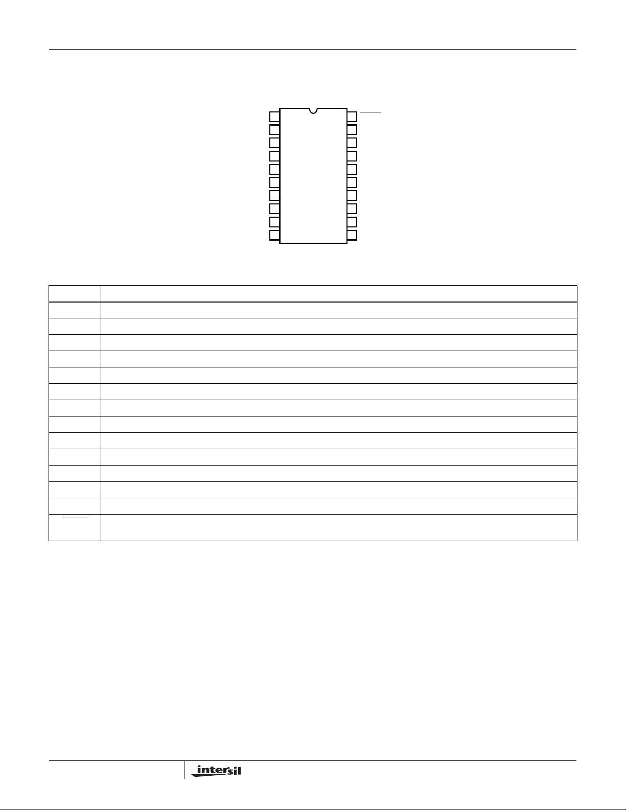
Pinout
www.BDTIC.com/Intersil
ISL83386E
ISL83386E (TSSOP)
TOP VIEW
C1+
1
V+
2
C1-
3
C2+
4
C2-
5
6
V-
T1
7
IN
T2
8
IN
9
T3
IN
10
R2
OUT
Pin Descriptions
PIN FUNCTION
V
CC
V+ Internally generated positive transmitter supply (+5.5V).
V- Internally generated negative transmitter supply (-5.5V).
GND Ground connection.
C1+ External capacitor (voltage doubler) is connected to this lead.
C1- External capacitor (voltage doubler) is connected to this lead.
C2+ External capacitor (voltage inverter) is connected to this lead.
C2- External capacitor (voltage inverter) is connected to this lead.
T
T
OUT
R
R
OUT
V
SHDN
System power supply input (3.0V to 5.5V).
TTL/CMOS compatible transmit ter I nput s . The switching point is a function of the VL voltage.
IN
±15kV ESD Protected, RS-232 level (nominally ±5.5V) transmitter outputs.
±15kV ESD Protected, RS-232 compatible receiver in puts.
IN
TTL/CMOS level receiver outputs. Swings between GND and VL.
Logic-Level Supply. All TTL/CMOS inputs and outputs are powered by this supply.
L
Active low TTL/C MOS input to tri-state receiver and tr ansmitter outputs and to shut down the on-board power supply to place de vice
in low power mode. The switching point is a function of the V
voltage.
L
SHDN
20
V
19
CC
18
GND
T1
17
OUT
T2
16
OUT
T3
15
OUT
R1
14
IN
R2
13
IN
V
12
L
R1
11
OUT
2
FN6034.1
November 19, 2004

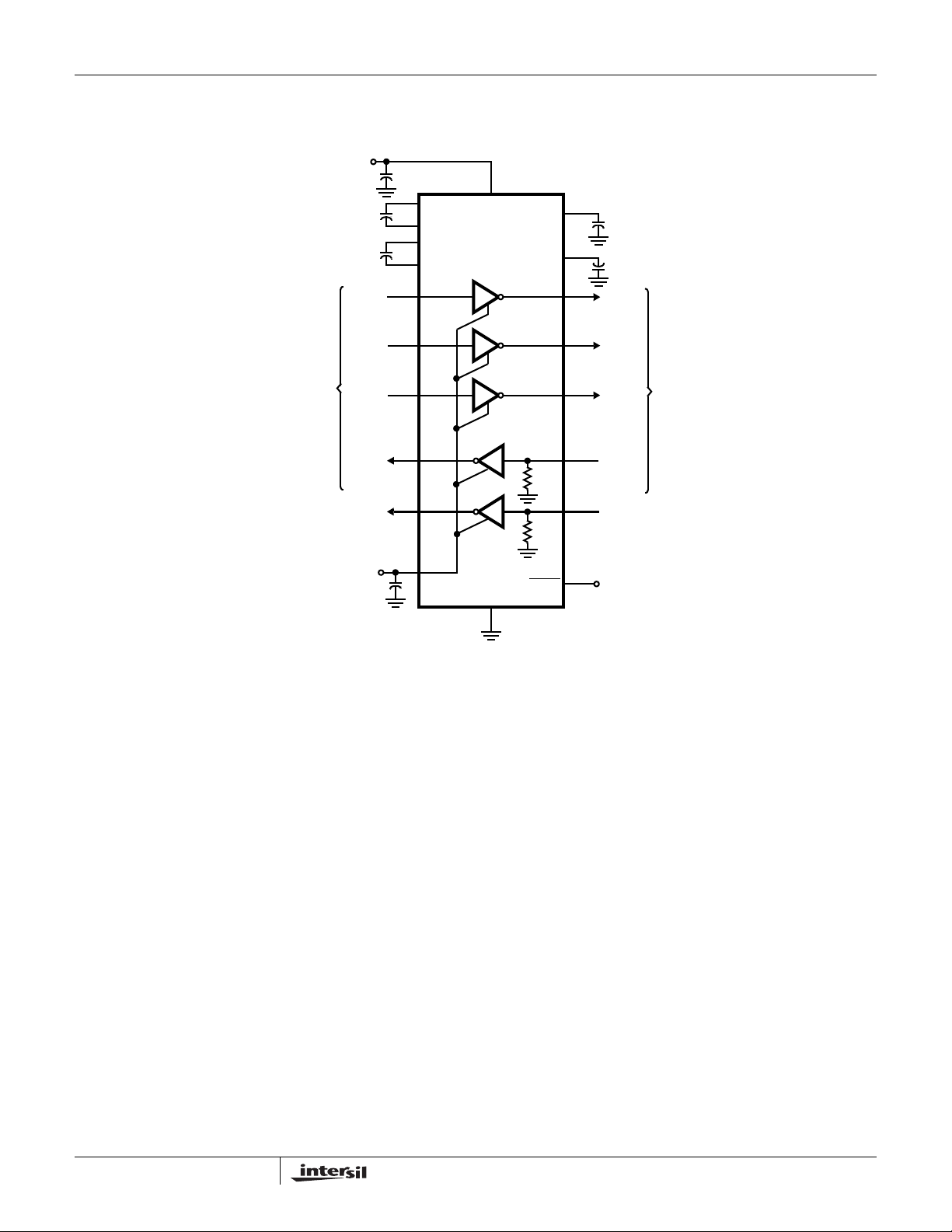
Typical Operating Circuit
www.BDTIC.com/Intersil
ISL83386E
+3.3V to +5V
TTL/CMOS
LOGIC LEVELS
LOGIC V
C
0.1µF
C
0.1µF
T1
T2
T3
R1
OUT
R2
OUT
CC
0.1µF
+
0.1µF
1
1
2
IN
IN
IN
C1+
+
3
C1-
4
C2+
+
5
C2-
7
8
9
11
10
V
12
L
+
V
CC
R
R
GND
19
2
C
3
V+
V-
T
1
T
2
T
3
1
5kΩ
2
5kΩ
SHDN
18
+
0.1µF
6
C
4
0.1µF
+
17
T1
OUT
16
T2
OUT
OUT
IN
IN
RS-232
LEVELS
15
T3
14
R1
13
R2
20
V
CC
3
FN6034.1
November 19, 2004
 Loading...