®
www.BDTIC.com/Intersil
ISL83384E
Data Sheet March 15, 2005
±15kV ESD Protected, +3V to +5.5V,
1 Microamp, 250Kbps, RS-232
Transmitter/Receiver
The Intersil ISL83384E contains 3.0V to 5.5V powered
RS-232 transmitters/receivers which meet ElA/TIA-232 and
V.28/V.24 specifications, even at V
applications are PDAs, Palmtops, and notebook and laptop
computers where the low operational, and even lower
standby, power consumption is critical. Efficient on-chip
charge pumps, coupled with a manual powerdown function
reduces the standby supply current to a 1µA trickle. Small
footprint packaging, and the use of small, low value
capacitors ensure board space savings as well. Data rates
greater than 250Kbps are guaranteed at worst case load
conditions. This device is fully compatible with 3.3V only
systems, mixed 3.3V and 5.0V systems, and 5.0V only
systems.
The single pin powerdown function (SHDN
the transmitters and receivers, while shutting down the
charge pump to minimize supply current drain.
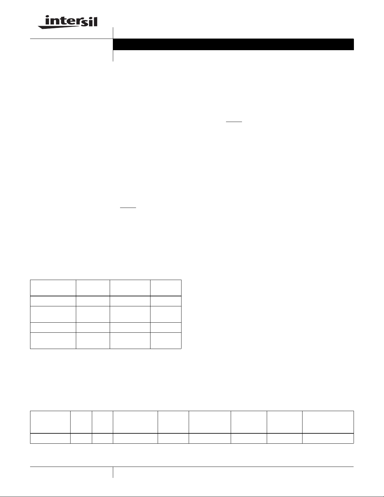
Table 1 summarizes the features of the ISL83384E, while
Application Note AN9863 summarizes the features of each
device comprising the ICL32XX 3V family.
= 3.0V. Targeted
CC
= 0) disables all
FN6017.3
Features
• ESD Protection for RS-232 I/O Pins to ±15kV (IEC61000)
• Drop In Replacement for MAX3384E, SP385E
• Low Power, Pin Compatible Upgrade for 5V MAX222,
SP310E, ADM222, and LT1780
• Single SHDN
• Meets EIA/TIA-232 and V.28/V.24 Specifications at 3V
• RS-232 Compatible with V
• Latch-Up Fre e
• On-Chip Voltage Converters Require Only Four External
0.1µF Capacitors
• Receiver Hysteresis For Improved Noise Immunity
• Very Low Supply Current . . . . . . . . . . . . . . . . . . . . 0.3mA
• Guaranteed Minimum Data Rate . . . . . . . . . . . . 250Kbps
• Guaranteed Minimum Slew Rate. . . . . . . . . . . . . . . 6V/µs
• Wide Power Supply Range. . . . . . . . Single +3V to +5.5V
• Low Supply Current in Powerdown State. . . . . . . . . .<1µA
• Pb-Free Available (RoHS Compliant)
Pin Disables Transmitters and Receivers
= 2.7V
CC
Applications
Ordering Information
PART NUMBER
ISL83384ECA 0 to 70 20 Ld SSOP M20.209
ISL83384ECAZA
(See Note)
ISL83384ECA-T 0 to 70 Tape and Reel M20.209
ISL83384ECAZA-T
(See Note)
NOTE: Intersil Pb-free products employ special Pb-free material sets;
molding compounds/die attach materials and 100% matte tin plate
termination finish, which are RoHS compliant and compatible with
both SnPb and Pb-free soldering operations. Intersil Pb-free products
are MSL classified at Pb-free peak reflow temperatures that meet or
exceed the Pb-free requirements of IPC/JEDEC J STD-020.
PART
NUMBER
ISL83384E 2 2 0 250 NO NO YES NO
TEMP.
RANGE (°C) PACKAGE
0 to 70 20 Ld SSOP
0 to 70 Tape and Reel
NO. OF
Tx.
NO. OF
Rx.
(Pb-free)
(Pb-free)
MONITOR Rx.
NO. OF
(R
OUTB
PKG.
DWG. #
M20.209
M20.209
TABLE 1. SUMMARY OF FEATURES
DATA
)
RATE
(Kbps)
• Any System Requiring RS-232 Communication Ports
- Battery Powered, Hand-Held, and Portable Equipment
- Laptop Computers, Notebooks, Palmtops
- Modems, Printers and other Peripherals
- Digital Cameras
- Cellular/Mobile Phones
Related Literature
• Technica l Brief TB363 “Guidelines for Handling and
Processing Moisture Sensitive Surface Mount Devices
(SMDs)”
• AN9863, “3V to +5.5V, 250k-1Mbps, RS-232
Transmitters/Receivers”
MANUAL
Rx. ENABLE
FUNCTION?
READY
OUTPUT?
POWER-
DOWN?
POWERDOWN
AUTOMATIC
FUNCTION?
1
CAUTION: These devices are sensitive to electrostatic discharge; follow proper IC Handling Procedures.
1-888-INTERSIL or 321-724-7143
| Intersil (and design) is a registered trademark of Intersil Americas Inc.
Copyright © Intersil Americas Inc. 2001, 2003, 2004, 2005. All Rights Reserved
All other trademarks mentioned are the property of their respective owners.

ISL83384E
www.BDTIC.com/Intersil
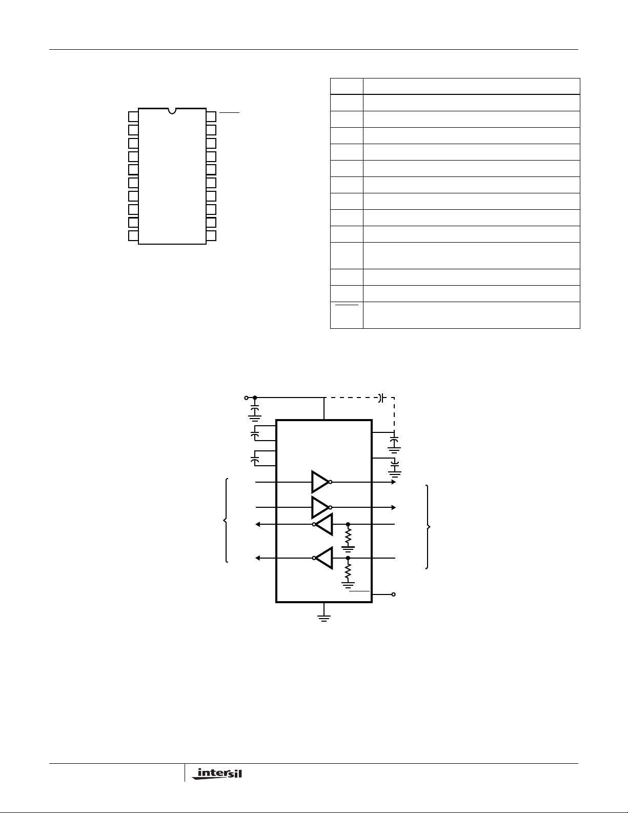
Pinout
ISL83384E (SSOP)
TOP VIEW
NC
1
C1+
2
3
V+
C1-
4
C2+
5
C2-
6
V-
7
T2
8
OUT
R2
9
IN
10
NC
Typical Operating Circuit
TTL/CMOS
LOGIC LEVELS
20
SHDN
V
19
CC
GND
18
17
T1
OUT
R1
16
IN
R1
15
OUT
T1
14
IN
T2
13
IN
12
R2
OUT
NC
11
+3.3V to +5V
0.1µF
0.1µF
R1
R2
C
C
T1
T2
OUT
OUT
Pin Descriptions
PIN FUNCTION
VCCSystem power supply input (3.0V to 5.5V).
V+ Internally generated positive transmitter supply (+5.5V).
V- Internally generated negative transmitter supply (-5.5V).
GND Ground connection.
C1+ External capacitor (voltage doubler) is connected to this lead.
C1- External cap acitor (voltage doubler) is connected to this lead.
C2+ External capacitor (voltage inverter) is connected to this lead.
C2- External capa citor (voltage inverter) is connected to this lead.
TTL/CMOS compatible transmitter Inputs.
T
IN
±15kV ESD Protected, RS-232 level (nominally ±5.5V)
T
OUT
transmitter outputs.
±15kV ESD Protected, RS-232 compatible receiver inputs.
R
IN
R
TTL/CMOS level receiver outputs.
OUT
Active low input to shut down transmitters, receivers, and
SHDN
on-board power supply, to place device in low power mode.
ISL83384E
C3 (OPTIONAL CONNECTION, NOTE 1)
+
0.1µF
2
1
2
IN
IN
C1+
+
4
C1-
5
C2+
+
6
C2-
14
13
15
12
19
V
CC
T
T
R
1
R
2
V+
V-
1
2
5kΩ
5kΩ
+
3
C
3
+
0.1µF
7
C
4
0.1µF
+
17
T1
OUT
8
T2
OUT
16
R1
9
R2
RS-232
LEVELS
IN
IN
20
GND
SHDN
18
NOTES:
1. The negative terminal of C
can be connected to either VCC or GND.
3
2
V
CC
FN6017.3
March 15, 2005

ISL83384E
www.BDTIC.com/Intersil
Absolute Maximum Ratings Thermal Information
VCC to Ground. . . . . . . . . . . . . . . . . . . . . . . . . . . . . . . . -0.3V to 6V
V+ to Ground . . . . . . . . . . . . . . . . . . . . . . . . . . . . . . . . . -0.3V to 7V
V- to Ground. . . . . . . . . . . . . . . . . . . . . . . . . . . . . . . . . +0.3V to -7V
V+ to V- . . . . . . . . . . . . . . . . . . . . . . . . . . . . . . . . . . . . . . . . . . . 14V
Input Voltages
, SHDN . . . . . . . . . . . . . . . . . . . . . . . . . . . . . . . . . -0.3V to 6V
T
IN
R
. . . . . . . . . . . . . . . . . . . . . . . . . . . . . . . . . . . . . . . . . . . . ±25V
IN
Output Voltages
. . . . . . . . . . . . . . . . . . . . . . . . . . . . . . . . . . . . . . . . . ±13.2V
T
OUT
R
. . . . . . . . . . . . . . . . . . . . . . . . . . . . . . . -0.3V to VCC +0.3V
OUT
Short Circuit Duration
. . . . . . . . . . . . . . . . . . . . . . . . . . . . . . . . . . . . . Continuous
T
OUT
ESD Rating . . . . . . . . . . . . . . . . . . . . . . . . . See Specification Table
CAUTION: Stresses above those listed in “Absolute Maximum Ratings” may cause permanent damage to the device. This is a stress only rating and operation of the
device at these or any other conditions above those indicated in the operational sections of this specification is not implied.
NOTE:
2. θ
is measured with the component mounted on a low effective thermal conductivity test board in free air. See Tech Brief TB379 for details.
JA
Thermal Resistance (Typical, Note 2)
20 Ld SSOP Package . . . . . . . . . . . . . . . . . . . . . . . 125
Maximum Junction Temperature (Plastic Package) . . . . . . . 150°C
Maximum Storage Temperature Range. . . . . . . . . . .-65°C to 150°C
Maximum Lead Temperature (Soldering 10s) . . . . . . . . . . . . 300°C
(Lead Tips Only)
θ
JA
(°C/W)
Operating Conditions
Tem perature Range
ISL83384ECX . . . . . . . . . . . . . . . . . . . . . . . . . . . . . 0°C to 70°C
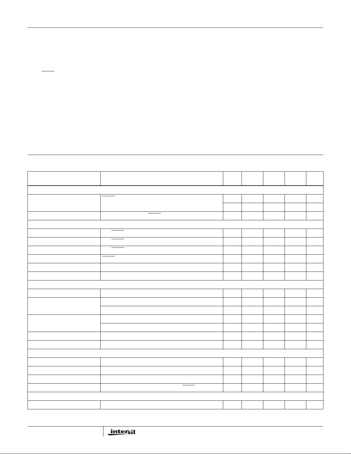
Electrical Specifications Test Conditions: V
Typicals are at T
PARAMETER TEST CONDITIONS
DC CHARACTERISTICS
Supply Current, Powerdown SHDN
Supply Current, Enabled All Outputs Unloaded, SHDN
LOGIC AND TRANSMITTER INPUTS AND RECEIVER OUTPUTS
Input Logic Threshold Low T
Input Logic Threshold High T
Input Leakage Current T
Output Leakage Current SHDN
Output Voltage Low I
Output Voltage High I
RECEIVER INPUTS
Input Voltage Range Full -25 - 25 V
Input Threshold Low V
Input Threshold High V
Input Hysteresis Full 0.2 0.5 1 V
Input Resistance Full 3 5 7 kΩ
TRANSMITTER OUTPUTS
Output Voltage Swing All Transmitter Outputs Loaded with 3kΩ to Ground Full ±5.0 ±5.4 - V
Output Resistance V
Output Short-Circuit Current Full ±7 ±35 - mA
Output Leakage Current V
TIMING CHARACTERISTICS
Maximum Data Rate R
= GND 25 - 0.1 5 µA
, SHDN Full - - 0.8 V
IN
, SHDN Full 2.4 - - V
IN
, SHDN Full - ±0.01 ±1.0 µA
IN
= GND Full - ±0.05 ±10 µA
= 3.2mA Full - - 0.4 V
OUT
= -1.0mA Full V
OUT
= 3.3V 25 0.6 1.2 - V
CC
= 5.0V Full 0.8 1.5 - V
V
CC
= 3.3V 25 - 1.5 2.4 V
CC
= 5.0V Full - 1.8 2.4 V
V
CC
= V+ = V- = 0V, Transmitter Output = ±2V Full 300 10M - Ω
CC
= ±12V, VCC = 0V or 3V to 5.5V, SHDN = GND Full - - ±10 µA
OUT
= 3kΩ, CL = 1000pF, One Transmitter Switching Full 250 500 - Kbps
L
= 3V to 5.5V, C1 - C4 = 0.1µF; Unless Otherwise Specified.
CC
= 25°C
A
TEMP
(°C) MIN TYP MAX UNITS
Full - 1 50 µA
= V
CC
Full - 0.3 3.0 mA
CC
-0.6 V
-0.1 - V
CC
3
FN6017.3
March 15, 2005
 Loading...