intersil ISL83202 DATA SHEET

®
www.BDTIC.com/Intersil
ISL83202
Data Sheet FN6382.0
55V, 1A Peak Current H-Bridge FET Driver
The ISL83202 is a medium-frequency H-Bridge FET driver
capable of 1A (typ) of peak drive current that is designed to
drive high- and low-side N-Channel MOSFETs in mediumvoltage applications. Optimized for PWM motor control and
uninterruptible power supply systems, the ISL83202 enables
simple and flexible bridge-based design. With typical inputto-output propagation delays as low as 25ns and with a userprogrammable dead-time range of 0.1µs to 4.5µs, the
ISL83202 is ideal for switching frequencies up to 200kHz.
The dead-time of the ISL83202 is programmable via a single
resistor. The ISL83202's four independent driver control
inputs (ALI, AHI, BLI, and BHI) allow driving of every
possible switch combination except those that would cause
a shoot-through condition. A global disable input, DIS,
overrides input control and causes the ISL83202 to refresh
the bootstrap capacitor when pulled low. Integrated
undervoltage protection and shoot-through protection ensure
reliable system operation.
The ISL83202 is available in compact 16 Ld SOIC and 16 Ld
PDIP packages and operates over the range of -55°C to
+125°C.
Ordering Information
PART
NUMBER
ISL83202IBZ
(Note)
ISL83202IBZT
(Note)
ISL83202IPZ
(Note)
NOTE: Intersil Pb-free plus anneal products employ special Pb-free
material sets; molding compounds/die attach materials and 100%
matte tin plate termination finish, which are RoHS compliant and
compatible with both SnPb and Pb-free soldering operations. Intersil
Pb-free products are MSL classified at Pb-free peak reflow
temperatures that meet or exceed the Pb-free requirements of IPC/
JEDEC J STD-020.
**Pb-free PDIPs can be used for through hole wave solder processing
only. They are not intended for use in Reflow solder processing
applications.
PART
MARKING
83202IBZ -55 to +125 16 Ld SOIC (N)
16 Ld SOIC (N) Tape and Reel
(Pb-free)
ISL83202IPZ -55 to +125 16 Ld PDIP**
TEMP.
RANGE (°C) PACKAGE
(Pb-free)
(Pb-free)
PKG.
DWG . #
M16.15
M16.15
E16.3
December 20, 2006
Features
• Independently Drives 4 N-Channel FETs in Half Bridge or
Full Bridge Configurations
• Bootstrap Supply Max Voltage: 70VDC
• Drives a 1000pF Load in Free Air at +50°C with Rise and
Fall Times of 15ns (typ)
• User-Programmable Dead Time from 0.1 to 4.5μs
• DIS (Disable) Overrides Input Control and Refreshes
Bootstrap Capacitor when Pulled Low
• Input Logic Thresholds Compatible with 5V to 15V Logic
Levels
• Shoot-Through Protection
• Undervoltage Protection
• Pb-Free Plus Anneal Available (RoHS Compliant)
Applications
• UPS Systems
• DC Motor Controls
• Full Bridge Power Supplies
• Switching Power Amplifiers
• Noise Cancellation Systems
• Battery Powered Vehicles
• Peripherals
• Medium/Large Voice Coil Motors
• Related Literature
- TB363, Guidelines for Handling and Processing
Moisture Sensitive Surface Mount Devices (SMDs)
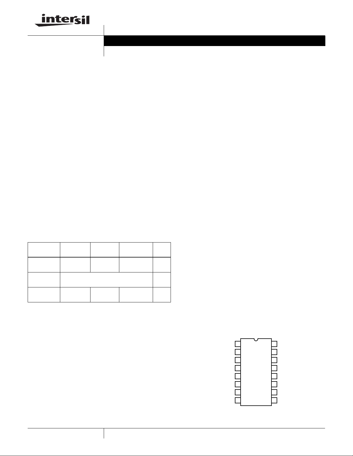
Pinout
ISL83202
(PDIP, SOIC)
TOP VIEW
16
BHB
BHI
BLI
ALI
DEL
V
SS
AHI
DIS
1
2
3
4
5
6
7
8
BHO
BHS
15
14
BLO
13
ALO
V
12
DD
11
AHS
AHO
10
9
AHB
1
CAUTION: These devices are sensitive to electrostatic discharge; follow proper IC Handling Procedures.
1-888-INTERSIL or 1-888-468-3774
| Intersil (and design) is a registered trademark of Intersil Americas Inc.
All other trademarks mentioned are the property of their respective owners.
Copyright Intersil Americas Inc. 2006. All Rights Reserved

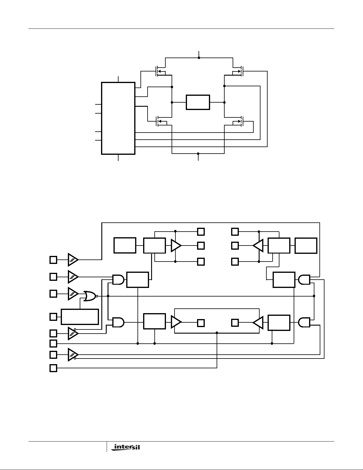
Application Block Diagram
www.BDTIC.com/Intersil
BHI
BLI
ISL83202
12V
BHO
BHS
BLO
ISL83202
55V
LOAD
ALI
AHI
Functional Block Diagram
BHI
2
AHI
7
DIS
8
12
UNDERVOLTAGE
4
5
DETECTOR
V
DD
ALI
DEL
GND
ALO
AHS
AHO
U/V
TURN-ON
DELAY
LEVEL
SHIFT
TURN-ON
DELAY
DRIVER
DRIVER
GND
10
11
13
AHB
9
AHO
AHS
ALO BLO
1
BHB
DRIVER
16
BHO
15
BHS
V
DD
DRIVER
14
LEVEL
SHIFT
TURN-ON
DELAY
TURN-ON
DELAY
U/V
BLI
3
V
6
SS
2
FN6382.0
December 20, 2006

ISL83202
www.BDTIC.com/Intersil
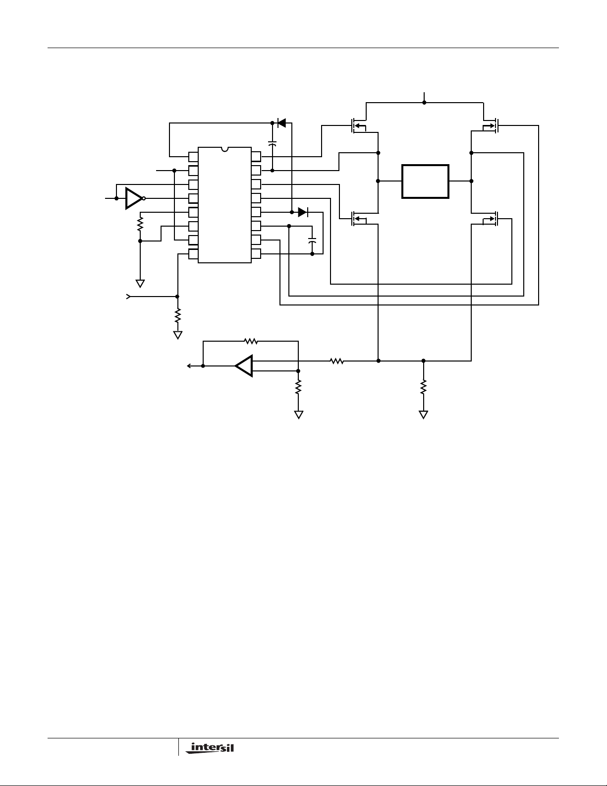
Typical Application (PWM Mode Switching)
16
BHO
BHS
15
14
BLO
13
ALO
V
AHS
SS
AHO
AHB
DD
12V
12
11
10
9
PWM
INPUT
DELAY RESISTOR
12V
DIS
1
BHB
2
BHI
3
BLI
4
ALI
5
DEL
6
V
7
AHI
8
DIS
55V
LOAD
FROM
OPTIONAL
OVERCURRENT
LATCH
TO OPTIONAL
CURRENT CONTROLLER OR
OVERCURRENT LATCH
GND
R
DIS
+
-
R
SH
GND
3
FN6382.0
December 20, 2006

ISL83202
www.BDTIC.com/Intersil
Absolute Maximum Ratings Thermal Information
Supply Voltage, VDD . . . . . . . . . . . . . . . . . . . . . . . . . . .-0.3V to 16V
Logic I/O Voltages . . . . . . . . . . . . . . . . . . . . . . . -0.3V to V
Voltage on AHS, BHS . . . . -6V (Transient) to 65V (-55°C to+150°C)
Voltage on AHB, BHB . . . . . . . . V
AHS, BHS
-0.3V to V
DD
AHS, BHS
+0.3V
+V
DD
Voltage on ALO, BLO. . . . . . . . . . . . . . . . . .VSS -0.3V to VDD +0.3V
Voltage on AHO, BHO. . . V
Current, DEL . . . . . . . . . . . . . . . . . . . . . . . . . . . . . . . . -5mA to 0mA
AHS, BHS
-0.3V to V
AHB, BHB
+0.3V Input
Phase Slew Rate . . . . . . . . . . . . . . . . . . . . . . . . . . . . . . . . . . 20V/ns
NOTE: All voltages are relative V
unless otherwise specified.
SS
Operating Conditions
Supply Voltage, VDD . . . . . . . . . . . . . . . . . . . . . . . . . +8.5V to +15V
Voltage on V
Voltage on AHB, BHB . . . . . . . . . . . . . . . . . . . . . . . . . . -1V to +55V
Voltage on AHB, BHB . . . . . . . .V
Input Current, DEL . . . . . . . . . . . . . . . . . . . . . . . . . -4mA to -100μA
CAUTION: Stresses above those listed in “Absolute Maximum Ratings” may cause permanent damage to the device. This is a stress only rating and operation of the
device at these or any other conditions above those indicated in the operational sections of this specification is not implied.
+150°C max junction temperature is intended for short periods of time to pr event sho rte ning the lif etime. Opera tio n close to +150° C ju nction ma y t rigger the shu t down of
the device even before +150°C, since this number is specified as typical.
. . . . . . . . . . . . . . . . . . . . . . . . . . . . . . -1.0V to +1.0V
SS
+7.5V to V
AHS, BHS
AHS, BHS +VDD
Thermal Resistance θ
JA
(°C/W)
SOIC Package . . . . . . . . . . . . . . . . . . . . . . . . . . . . . 115
PDIP Package* . . . . . . . . . . . . . . . . . . . . . . . . . . . . 90
Maximum Power Dissipation. . . . . . . . . . . . . . . . . . . . . . . . See Curve
Storage Temperature Range . . . . . . . . . . . . . . . . . .-65°C to +150°C
Operating Max. Junction Temperature. . . . . . . . . . . . . . . . . . +150°C
Lead Temperature (Soldering 10s) . . . . . . . . . . . . . . . . . . . . +300°C
(For SOIC - Lead Tips Only))
*Pb-free PDIPs can be used for through hole wave solder
processing only. They are not intended for use in Reflow solder
processing applications.
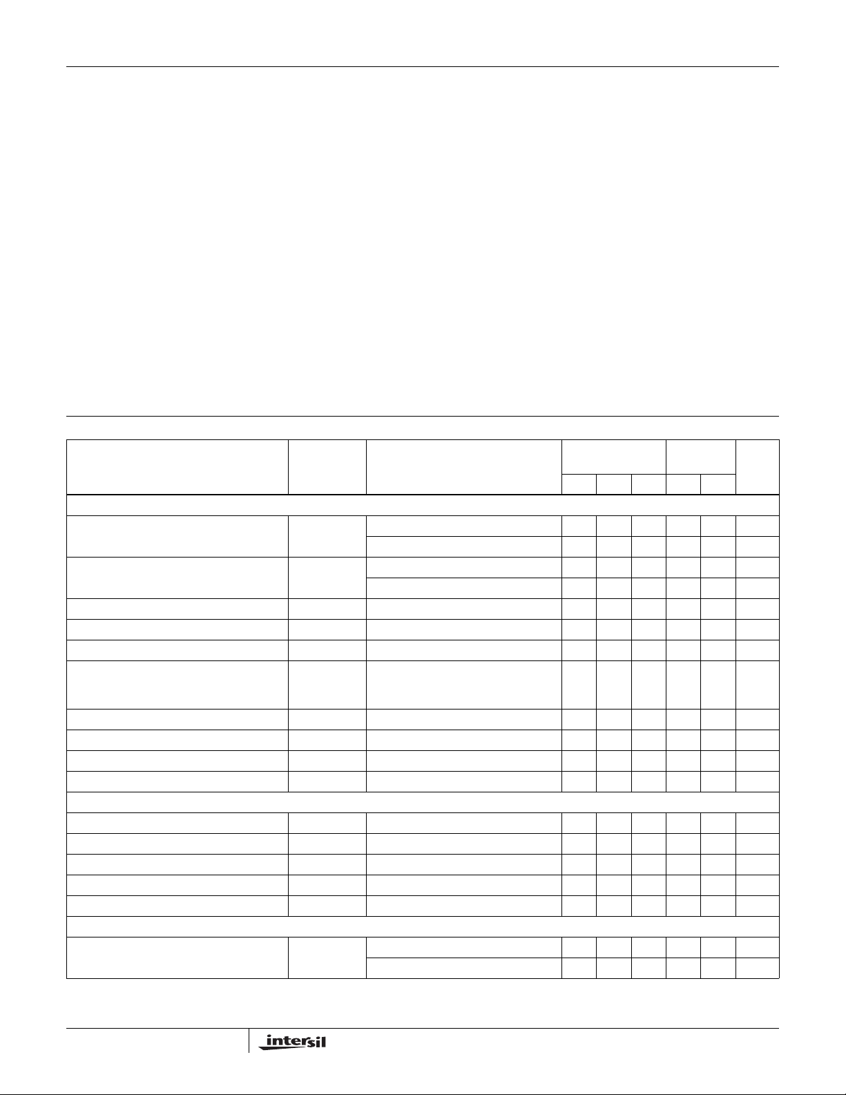
Electrical Specifications V
PARAMETER SYMBOL TEST CONDITIONS
DD
= V
AHB
= V
BHB
= 12V, VSS = V
AHS
= V
BHS
= 0V, R
DEL
= 100k
T
= +25°C
J
T
= -55°C
J
TO +150°C
UNITSMIN TYP MAX MIN MAX
SUPPLY CURRENTS AND UNDER VOLTAGE PROTECTION
Quiescent Current I
V
DD
Operating Current I
V
DD
AHB, BHB Off Quiescent Current I
AHB, BHB On Quiescent Current I
AHB, BHB Operating Current I
AHBL
AHBH
AHBO
AHS, BHS Leakage Current I
V
Rising Undervoltage Threshold V
DD
Falling Undervoltage Threshold V
V
DD
DD
DDO
, I
, I
, I
HLK
DDUV+
DDUV-
All inputs = 0V, R
All inputs = 0V, R
= 100k 1.2 2.3 3.5 0.85 4 mA
DEL
= 10k 2.2 4.0 5.5 1.9 6.0 mA
DEL
f = 50kHz, no load 1.5 2.6 4.0 1.1 4.2 mA
50kHz, no load, R
AHI = BHI = 0V 0.5 1.0 1.5 0.4 1.6 mA
BHBL
AHI = BHI = V
BHBH
f = 50kHz, CL = 1000pF .65 1.1 1.8 .45 2.0 mA
BHBO
V
= V
= V
BHS
BHB
= 55V
= 70V
AHS
V
AHB
= Not Connected
V
DD
= 10kΩ 2.5 4.0 6.4 2.1 6.6 mA
DEL
DD
65 145 240 40 250 μA
--1.0--μA
6.8 7.6 8.25 6.5 8.5 V
6.5 7.1 7.8 6.25 8.1 V
Undervoltage Hysteresis UVHYS 0.17 0.4 0.75 0.15 0.90 V
AHB, BHB Undervoltage Threshold VHBUV Referenced to AHS and BHS 5 6.0 7 4.5 7.5 V
INPUT PINS: ALI, BLI, AHI, BHI, and DIS
Low Level Input Voltage V
High Level Input Voltage V
IL
IH
Full Operating Conditions - - 1.0 - 0.8 V
Full Operating Conditions 2.5 - - 2.7 V
Input Voltage Hysteresis -35- - - mV
Low Level Input Current I
High Level Input Current I
IL
IH
VIN = 0V, Full Operating Conditions -145 -100 -60 -150 -50 μA
VIN = 5V, Full Operating Conditions -1 - +1 -10 +10 μA
TURN-ON DELAY PIN DEL
R
Dead Time T
DEAD
= 100k 2.5 4.5 8.0 2.0 8.5 μs
DEL
= 10k 0.27 0.5 0.75 0.2 0.85 μs
R
DEL
4
FN6382.0
December 20, 2006
 Loading...