

Page 1

Application Note 1386
ISL8201M, ISL8204M, ISL8206M EVAL1Z
Evaluation Board User’s Guide
Table of Contents
General Description.......................... .................................... ......................................................................................................... 2
Installation..................................................................................................................................................................................... 2
Typical Application Schematic....................................................................................................................................................... 3
Efficiency and Output Ripple/Noise Measurement........................................................................................................................ 4
Schematic ..................................................................................................................................................................................... 5
Bill of Materials.............................................................................................................................................................................. 6
Printed Circuit Board Layer........................................................................................................................................................... 7
List of Figures
Evaluation Board of POL Module.................................................................................................................................................. 2
Quick Start............................................................ .. ....................................................................................................................... 3
Quick Start Schematic............................................................................................ ....................................................................... 3
Wide Input Range Schematic........................................................................................................................................................ 3
Efficiency Measurement Schematic.............................................................................................................................................. 4
Equipment Setup for Efficiency Measurement.............................................................................................................................. 4
Output Ripple/Noise Measurement Method.................................................................................................................................. 4
Schematic ..................................................................................................................................................................................... 5
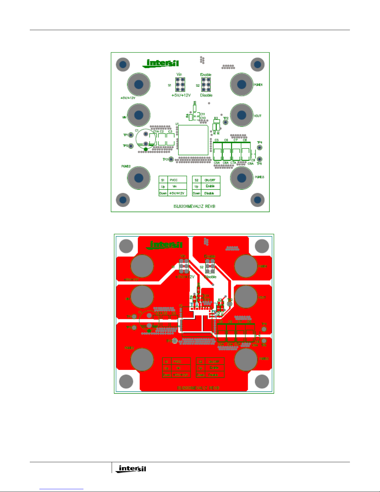
Top-Over Layer (Component Location).. ..... ... ... ............................................................................................................................ 7
Top Layer (Component Side)........................................................................................................................................................ 7
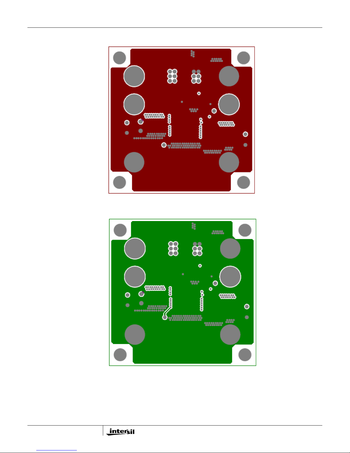
Middle-1 Layer............................................................................................................................................................................... 8
Middle-2 Layer............................................................................................................................................................................... 8
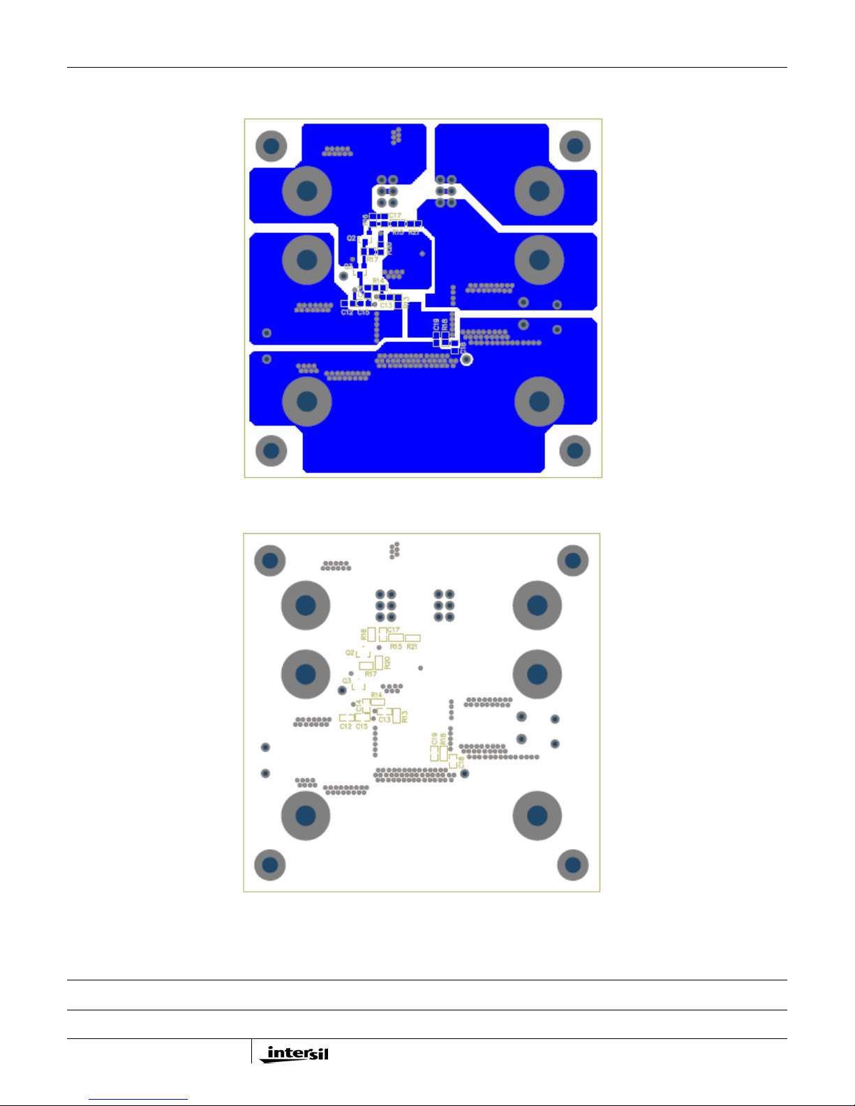
Bottom Layer (Component Side)................................................................................................................................................... 9
Bottom-Over Layer (Component Location)................................................................................................................................... 9
List of Tables
Test Equipment List................................ .. ...................................................................... ............................................................... 2
Recommended Operating Specifications...................................................................................................................................... 2
Typical Output Voltage Setting for each Resistance ..................................................................................................................... 2
Bill of Materials.............................................................................................................................................................................. 6
December 23, 2009
AN1386.1
1
CAUTION: These devices are sensitive to electrostatic discharge; follow proper IC Handling Procedures.
1-888-INTERSIL or 1-888-468-3774
| Intersil (and design) is a registered trademark of Intersil Amer ic as Inc .
All other trademarks mentioned are the property of their respective owners.
Copyright Intersil Americas Inc. 2009. All Rights Reserved
Page 2
Application Note 1386
General Description
This app note covers the ISL8201MEVAL1Z,
ISL8204MEVAL1Z, ISL8206MEVAL1Z evaluation boards.
Since the modules are a pin for pin drop in with all
necessary unique circuitry integrated in the module, the
only difference in the BOM is the ISL8201M, ISL8206M,
or ISL8204M POL modules. We will refer to a generic
eval board, ISL820xMEVAL1Z to cover all three power
modules.
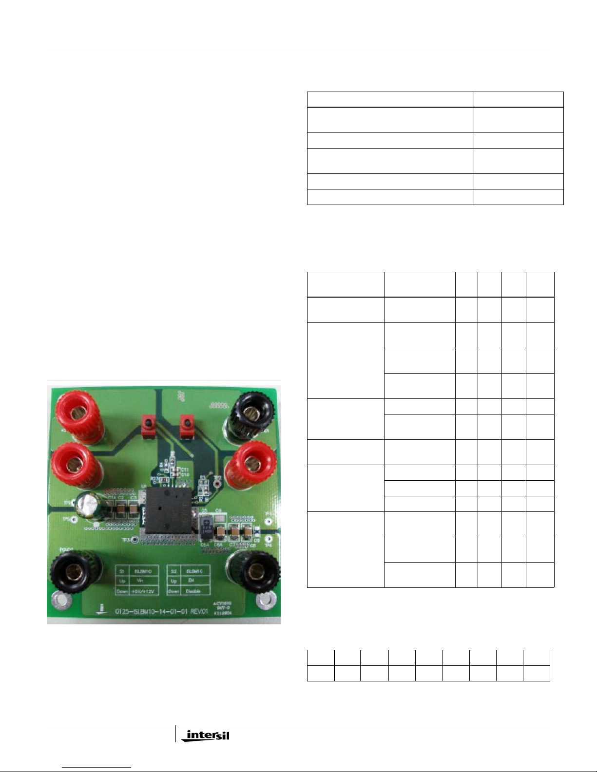
The ISL820xMEVAL1Z POL module evaluation board is
shown in Figure 1. The user can use it to evaluate the
performance of the Intersil ISL8201M, ISL8206M, or
ISL8204M POL modules. This board consists of power
and load connectors for source and load side, switches
for PVCC bias selection and On/Off option, and other
passive components.
The input voltage range is from 1V to 20V, and the
output voltage range is from 0.6V to 5V 5V for the
ISL8201M or 0.6V to 6V for the ISL8204M and
ISL8206M. Additional PVCC bias source is not required
when using an input voltage of 5V or 12V. It can
connect to the input side directly . However, in wider
input ranges, which are above 14V or below 5V, the
PVCC bias needs to add an external source, which
provides operation bias of the module . The output
voltage is initially set at 1 .5V for typic al ev aluati on. The
user can easily set the output voltage b y chang ing the
value of R
(refer to Figure 8).
1
Installation
TABLE 1. TEST EQUIPMENT LIST
EQUIPMENT PART NUMBER
An adjustable DC Power Supply 30V, 15A,
with current limit
An electronic load, capable of sinking 20A Chr oma 63030/63010
Four channel oscilloscope and probes Tektronix TDS3014
High Precision Digital Voltage Meter ESCORT 3136A
High Precision Digital Current Meter ESCORT 3136A
Recommended Operating Specification
The recommended operating specification for
input/output and PVCC bias range is shown as Table 2.
TABLE 2. RECOMMENDED OPERATING SPECIFICATIONS
TEST
PARAMETER
Input Voltage
Range (V
Supply Voltage
Range (PVCC)
Output Voltage
Range (V
Current Setting for
V
OUT
Output Current
(Load Current)
Current Limit
(PVCC = 12V)
IN
OUT
)
)
CONDITIONS MIN TYP MAX UNIT
Fixed +5V
Supply
Fixed +12V
Supply
Wide Range
Supply
ISL8201M 0.6 - 5 V
ISL8204M and
ISL8206M
R1 = 6.49kΩ -1.5- V
ISL8201M - - 10 A
ISL8206M - - 6 A
ISL8204M - - 4 A
ISL8201M
R
= 3.57kΩ
SEN-IN
ISL8206M
= 4.12kΩ
R
SEN-IN
ISL8204M
R
= 2.87kΩ
SEN-IN
GW GPC–3060D
Tektronix P3010
1-20V
4.5 5.0 5.5 V
9.6 12.0 14.4 V
6.5 - 14.4 V
0.6 - 6 V
-17- A
-8.8- A
-6.6- A
FIGURE 1. EVALUATION BOARD OF POL MODULE
2
Table 3 lists the typical application’s various output
voltages and its corresponding resistance.
TABLE 3. TYPICAL OUTPUT VOLTAGE SETTING FOR
V
OUT
R
1
EACH RESISTANCE
0.6V 1.05V 1.2V 1.5V 1.8V 2.5V 3.3V 5V
Open 13k 9.76k 6.49k 4.87k 3.09k 2.16k 1.33k
December 23, 2009
AN1386.1
Page 3
Application Note 1386
Selecting Switches
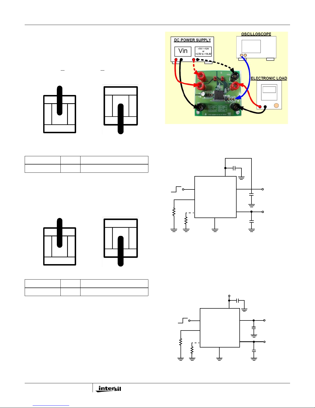
Switch S1 selects PVCC bias supply from VIN or an
additional supply source. When S1 is pushed up, the
PVCC bias connects to the input power side. When S1 is
pushed down, the PVCC bias connects to the additional
power supply. For typical applications, the PVCC bias
voltage is +5V (+
supply a wider range from +6.5V to +14.4V.
10%) or +12V (+20%). It can also
VIN
VIN
S1
+5V/+12V
OR
+6.5V TO +14.4V
S1
+6.5V TO +14.4V
+5V/+12V
OR
SWITCH UP DOWN
S1 V
+5V/+12V or +6.5V to +14.4V
IN
Switch S2 selects module Enable (On) or Disable (Off).
When S2 is pushed up, the COMP/EN pin of the module is
enabled and the module starts initialization and
operation. When S2 is pushed down, the COMP/EN pin of
the module connects to ground and the module will be
shut down.
EN
S2
ENABLE
S2
SWITCH UP DOWN
S2 EN Disable
EN
DISABLE
Quick Start
The evaluation board can be evaluated simply, as shown
in Figure 2. The power connection of the evaluation
board supplies the input voltage from the DC Power
Supply , and the load con nection of the evaluation board
delivers power to the Electronic Load. If the input voltage
is +5V or +12V, the PVCC bias does not require
additional supply and it can connect to the input side
directly by pushing switch S1 to the up state.
FIGURE 2. QUICK START FOR EVALUATION BOARD
Figure 3 shows the ISL820xMEVAL1Z application
schematic for +5V or +12V input voltage. The PVCC pin
can connect to the input supply directly.
C
PVCC
PVCC
COMP/EN
FB
R
FB
R
SEN-EX
ISET
PGND
VIN
PHASE
VOUT
VIN (+5V/+12V)
C
IN
VOUT
C
OUT
FIGURE 3. QUICK START SCHEMATIC
Typical Application Schematic
Typical Application with Separated Power
Supply
Figure 4 shows the ISL820xMEVAL1Z application
schematic for a wide input voltage from +1V to +20V.
The PVCC supply can source +5V/+12V or +6.5V to
+14.4V.
R
FB
R
SEN-EX
COMP/EN
FB
ISET
PGND
P
VCC
(+5V/+12V OR +6.5V TO +14.4V)
C
PVCC
PVCC
VIN
PHASE
VOUT
C
IN
VIN
(+1V TO +20V)
VOUT
C
OUT
3
FIGURE 4. WIDE INPUT RANGE SCHEMATIC
December 23, 2009
AN1386.1
Page 4
Application Note 1386
PVCC
C
PVCC
Vin
+
-
DC Source
PVCC
COMP/EN
FB
ISET
R
R
FB
SEN-EX
PGND
PHASE
VOUT
Vout
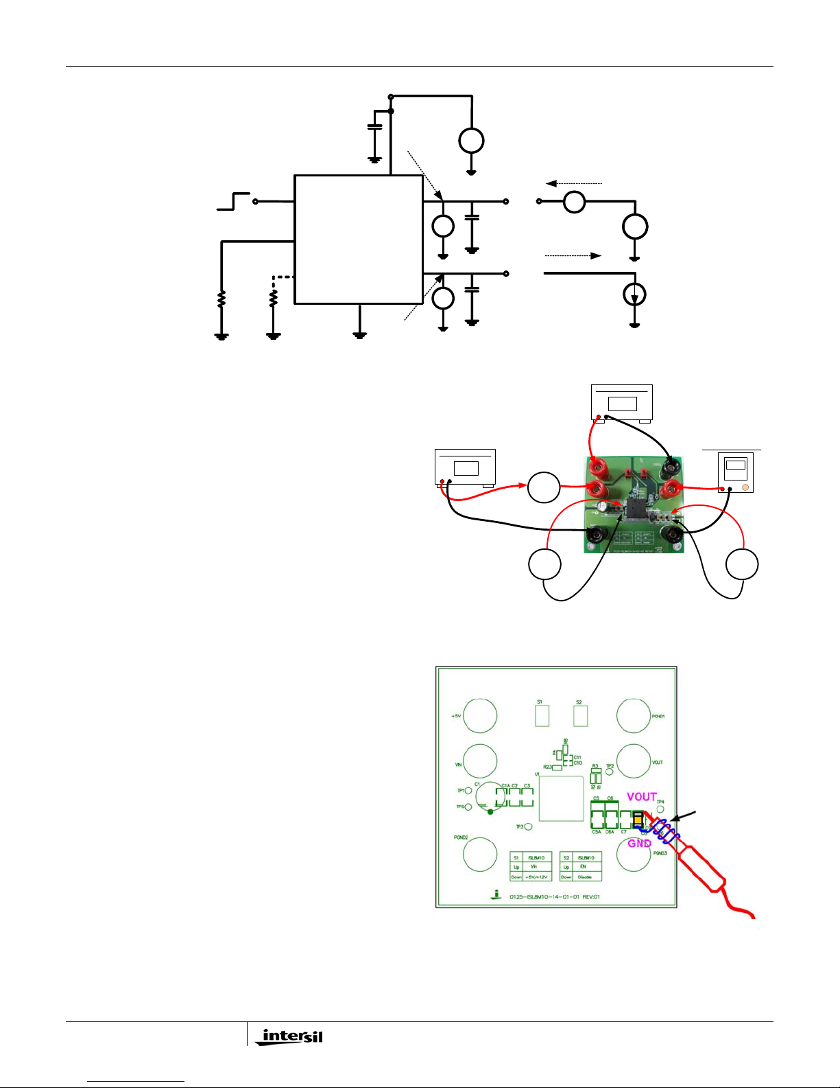
FIGURE 5. EFFICIENCY MEASUREMENT SCHEMATIC
Efficiency and Output
Ripple/Noise Measurement
Figure 5 shows the efficiency measurement schematic for
the ISL820xMEVAL1Z POL module. The voltage and
current meter can be used to measure input/output
voltage and current. In order to obtain an accurate
measurement and prevent the voltage drop of PCB or
wire trace, the voltage meter must be close to the
input/output pin of the POL module.
The efficiency equation is shown in Equation 1:
V
Efficiency
Output Power
------------------------------------
===
Input Power
P
OUT
--------------- -
P
IN
The equipment setup for the efficiency measurement on
the evaluation board is shown in Figure 6. The measuring
point for the input voltage meter is at the C
and the measuring point for the output voltage meter is
at the C
terminal (refer to Figure 9).
8
Output Ripple/Noise Measurement Method
The total noise is equal to the sum of the ripple and
noise components. Simple steps should be taken to
assure that there is minimum pickup noise due to the
high frequency even ts, w hic h can be magnified by the
large ground loop formed by the oscilloscope probe
ground. This means that even a few inches of ground
wire on the oscilloscope probe may result in hundreds of
millivolts of noise spikes when improperly routed or
terminated. This effect can be overcome by using the
short loop measurement method to minimize the
measurement loop area for reducing the pickup noise.
The short loop measurement method is shown in
Figure 7. For ISL820xMEVAL1Z evaluation board, the
output ripple/noise measurement point is located at the
terminal (refer to Figure 9).
C
8
•()
OUTIOUT
----------------------------------------
V
•()
INIIN
(EQ. 1)
terminal,
3
Iin
VIN
Vi
Vo
DC POWER SUPPLY
Vin
Cin
Cout
VIN
VOUT
Current
Meter
Ai
Iout
+
-
DC POWER SUPPLY
PVCC
DC Source
DC Load
+
Voltage
Meter
-
FIGURE 6. EQUIPMENT SETUP FOR EFFICIENCY
MEASUREMENT
FIGURE 7. OUTPUT RIPPLE/NOISE
MEASUREMENT METHOD
ELECTRONIC LOAD
Voltage
Meter
SHORT LOOP
MEASUREMENT
METHOD
+
-
4
December 23, 2009
AN1386.1
Page 5
5
AN1386.1
December 23, 2009
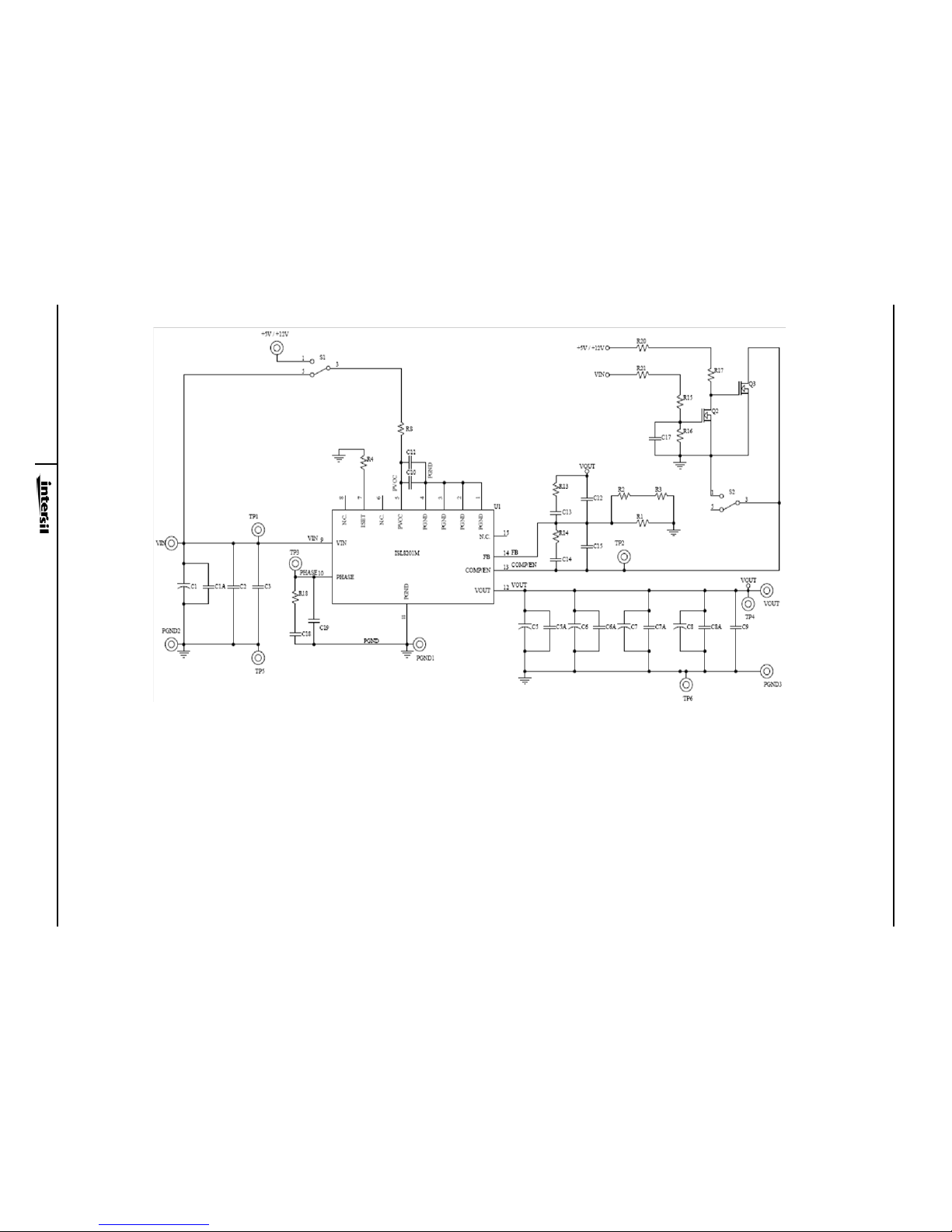
NOTES:
1. R
1
is used to set the output voltage of ISL820xMEVAL1Z. Initial setting is 6.49kΩ for 1.5V output voltage.
2. R
2
and R3, paralleling with R1, are used to adjust the output voltage of ISL820xMEVAL1Z.
3. R
4
is used to set the overcurrent trip lev el of ISL820xMEVAL1Z. The ISL8201MEVAL1 Z has int egr ate d 3. 57k Ω, ISL8206MEVAL1Z has integrated 4.12k Ω, and
ISL8204MEVAL1Z has integrated 2.87kΩ
4. R
18
, C18 and C19 are the snubber network, which can reduce the stress for internal semiconductor.
5. R
13
, R14, C12, C13, C14 and C15 are the external compensation network. The ISL820xMEVAL1Z has integrated the type 3 compensation network inside the module
for typical applications.
6. R
15
, R16, R17, R20, R21, C17, Q2 and Q3 are the power-up sequence circuit. In case of PVCC bias, power-up first, then input voltage. This circuit has to be implemented.
FIGURE 8. SCHEMATIC
Application Note 1386
Page 6

Application Note 1386
TABLE 4. BILL OF MATERIALS
SYMBOL COMPONENTS DESCRIPTION SUPPLIER
R1 Resistor Chip Resistor 6.49kΩ Generic
R2 Resistor Not installed R3 Resistor Not installed R4 Resistor Not installed -
R8 Resistor Chip Resistor 10Ω Generic
R13 Resistor Not installed R14 Resistor Not installed R15 Resistor Not installed R16 Resistor Not installed R17 Resistor Not installed R18 Resistor Not installed R20 Resistor Not installed R21 Resistor Not installed -
C1 Capacitor AL Capacitor 220µF/35V SANYO
C1A Capacitor Not installed -
C2 Capacitor Ceramic Capacitor 10µF/25V MURATA/TDK
C3 Capacitor Ceramic Capacitor 10µF/25V MURATA/TDK
C5 Capacitor POS Capacitor 330µF/6.3V SANYO
C5A Capacitor Not installed -
C6 Capacitor Not installed C6A Capacitor Ceramic Capacitor 22µF/10V MURATA/TDK
C7 Capacitor Ceramic Capacitor 22µF/10V MURATA/TDK
C7A Capacitor Not installed MURATA/TDK
C8 Capacitor Ceramic Capacitor 22µF/10V MURATA/TDK
C8A Capacitor Not installed -
C9 Capacitor Not installed C10 Capacitor Ceramic Capacitor 1µF/25V YAGEO
C11 Capacitor Ceramic Capacitor 1µF/25V YAGEO
C12 Capacitor Not installed C13 Capacitor Not installed C14 Capacitor Not installed C15 Capacitor Not installed C17 Capacitor Not installed C18 Capacitor Not installed C19 Capacitor Not installed -
S1 Switch UT Switch SH
S2 Switch UT Switch SH
Q2 MOSFET Not installed -
Q3 MOSFET Not installed -
U1 Module ISL8201M, ISL8206M, or ISL8204M Intersil
6
December 23, 2009
AN1386.1
Page 7
Application Note 1386
Printed Circuit Board Layers
FIGURE 9. TOP-OVER LAYER (COMPONENT LOCATION)
FIGURE 10. TOP LAYER (COMPONENT SIDE)
7
December 23, 2009
AN1386.1
Page 8
Application Note 1386
Printed Circuit Board Layers (Continued)
FIGURE 11. MIDDLE-1 LAYER
FIGURE 12. ISL820xMEVAL1Z, MIDDLE-2 LAYER
8
December 23, 2009
AN1386.1
Page 9
Application Note 1386
Printed Circuit Board Layers (Continued)
FIGURE 13. BOTTOM LAYER (COMPONENT SIDE MIRRORED)
FIGURE 14. BOTTOM-OVER LAYER (COMPONENT LOCATION MIRRORED)
Intersil Corporation reserves the right to make changes in circuit design, software and/or specifications at any time without notice. Accordingly, the
reader is cautioned to verify that the Applica tio n No te or Tec hnical Brief is current before proceeding.
For information regarding Intersil Corporation and its products, see www.intersil.com
9
December 23, 2009
AN1386.1
 Loading...