

查询ISL41334IRZ供应商
®
ISL81334, ISL41334
Data Sheet December 20, 2005
±15kV ESD Protected, Two Port, Dual
Protocol Transceivers
The ISLX1334 are two port interface ICs where each port
can be independently configured as a single RS-485/422
transceiver, or as a dual (2 Tx, 2 Rx) RS-232 transceiver.
With both ports set to the same mode, two RS-485/422
transceivers, or four RS-232 transceivers are available.
If either port is in RS-232 mode, the onboard charge pump
generates RS-232 compliant ±5V Tx output levels from a
single V
capacitors are required for the charge pump. The
transceivers are RS-232 compliant, with the Rx inputs
handling up to ±25V, and the Tx outputs handling ±12V.
In RS-485 mode, the transceivers support both the RS-485
and RS-422 differential communication standards. The
receivers feature "full failsafe" operation, so the Rx outputs
remain in a high state if the inputs are open or shorted
together. The transmitters support up to three data rates, two
of which are slew rate limited for problem free
communications. The charge pump disables when both
ports are in RS-485 mode, thereby saving power, minimizing
noise, and eliminating the charge pump capacitors.
Both RS-232 and RS-485 modes feature loopback and
shutdown functions. Loopback internally connects the Tx
outputs to the corresponding Rx input, to facilitate board
level self test implementation. The outputs remain connected
to the loads during loopback, so connection problems (e.g.,
shorted connectors or cables) can be detected. Shutdown
mode disables the Tx and Rx outputs, disables the charge
pumps, and places the IC in a low current (µA) mode.
The ISL41334 is a QFN packaged device that includes two
additional user selectable, lower speed and edge rate
options for EMI sensitive designs, or to allow longer bus
lengths. It also features a logic supply pin (V
V
OH
inputs, to be compatible with another supply voltage in mixed
voltage systems. The QFN also adds active low Rx enable
pins to increase design flexibility, allowing Tx/Rx direction
control, via a single signal per port, by connecting the
corresponding DE and RE
supply as low as 4.5V. Four small 0.1µF
CC
) that sets the
L
level of logic outputs, and the switching points of logic
pins together.
FN6202.1
Features
• ±15kV (HBM) ESD Protected Bus Pins (RS-232 or
RS-485)
• Two Independent Ports, Each User Selectable for RS-232
(2 Transceivers) or RS-485/422 (1 Transceiver)
• Flow-Through Pinouts Simplify Board Layouts
• Pb-Free Plus Anneal Available (RoHS Compliant)
• Large (2.7V) Differential V
for Improved Noise
OUT
Immunity in RS-485/422 Networks
• Full Failsafe (Open/Short) Rx in RS-485/422 Mode
• Loopback Mode Facilitates Board Self Test Functions
• User Selectable RS-485 Data Rates (ISL41334 Only)
- Fast Speed . . . . . . . . . . . . . . . . . . . . . . . . . . . . 20Mbps
- Slew Rate Limited. . . . . . . . . . . . . . . . . . . . . . . 460kbps
- Slew Rate Limited. . . . . . . . . . . . . . . . . . . . . . . 115kbps
• Fast RS-232 Data Rate . . . . . . . . . . . . . . . Up to 650kbps
• Low Current Shutdown Mode. . . . . . . . . . . . . . . . . . .42µA
• QFN Package Saves Board Space (ISL41334 Only)
• Logic Supply Pin (V
) Eases Operation in Mixed Supply
L
Systems (ISL41334 Only)
Applications
• Gaming Applications (e.g., Slot Machines)
• Single Board Computers
• Factory Automation
• Security Networks
• Industrial/Process Control Networks
• Level Translators (e.g., RS-232 to RS-422)
• Point of Sale Equipment
• Dual Channel RS-485 Interfaces
For a single port version of these devices, please see the
ISL81387/ ISL41387 data sheet.
TABLE 1. SUMMARY OF FEATURES
PAR T N U MBER
ISL81334 2 28 Ld SOIC, 28 Ld SSOP 20M 650 NO NONE YES
ISL41334 2 40 Ld QFN (6 x 6mm) 20M, 460k, 115k 650 YES L YES
NO. OF
PORTS
PACKAGE OPTIONS
1
RS-485 DATA
RATE (bps)
CAUTION: These devices are sensitive to electrostatic discharge; follow proper IC Handling Procedures.
1-888-INTERSIL or 1-888-468-3774
RS-232 DATA
RATE (kbps)
| Intersil (and design) is a registered trademark of Intersil Americas Inc.
All other trademarks mentioned are the property of their respective owners.
PIN?
V
L
Copyright © Intersil Americas Inc. 2005. All Rights Reserved.
ACTIVE H or L
Rx ENABLE?
LOW POWER
SHUTDOWN?
ISL81334, ISL41334
Ordering Information
PART NUMBER (NOTE) PART MARKING TEMP. RANGE (°C) PACKAGE (Pb-Free) PKG. DWG. #
ISL81334IAZ 81334IAZ -40 to 85 28 Ld SSOP M28.209
ISL81334IAZ-T 81334IAZ -40 to 85 28 Ld SSOP Tape and Reel M28.209
ISL81334IBZ ISL81334IBZ -40 to 85 28 Ld SOIC M28.3
ISL81334IBZ-T ISL81334IBZ -40 to 85 28 Ld SOIC Tape and Reel M28.3
ISL41334IRZ 41334IRZ -40 to 85 40 Ld QFN L40.6x6
ISL41334IRZ-T 41334IRZ -40 to 85 40 Ld QFN Tape and Reel L40.6x6
NOTE: Intersil Pb-free plus anneal products employ special Pb-free material sets; molding compounds/die attach materials and 100% matte tin plate
termination finish, which are RoHS compliant and compatible with both SnPb and Pb-free soldering operations. Intersil Pb-free products are MSL
classified at Pb-free peak reflow temperatures that meet or exceed the Pb-free requirements of IPC/JEDEC J STD-020.
Pinouts
ISL81334 (SOIC, SSOP)
TOP VIEW
ISL41334 (QFN)
TOP VIEW
C1+
C1-
V+
A1
B1
Y1
Z1
SEL1
SEL2
Z2
Y2
B2
A2
GND
C2+
1
2
3
4
5
6
7
8
9
10
11
12
13
14
28
27
26
25
24
23
22
21
20
19
18
17
16
15
C2-
V
CC
R
B1
R
A1
DZ1/DE1
D
Y1
LB
ON/OFF
D
Y2
DZ2/DE2
R
A2
R
B2
V-
V+
A1
B1
Y1
Z1
SEL1
SEL2
Z2
Y2
B2
NC
NCNCC1-
40
39 38 37 36 35 34 33 32 31
1
2
3
4
5
6
7
8
9
10
11 12 13 14 15 16 17 18 19 20
A2
NC
C1+
C2+
C2-
VCCNC
SPA
SPB
GND
GND
RXEN1
RXEN2
L
V
30
R
B1
29
R
A1
28
DZ1/DE
1
D
27
Y1
LB
26
ON/OFF
25
D
24
Y2
DZ2/DE
23
22
21
V-
NC
2
R
A2
R
B2
2
FN6202.1
December 20, 2005
ISL81334, ISL41334
TABLE 2. ISL81334 FUNCTION TABLE
INPUTS RECEIVER OUTPUTS DRIVER OUTPUTS
DE 1 or 2 R
0 1 N.A. ON ON ON ON ON RS-232
X 0 X High-Z High-Z High-Z High-Z OFF Shutdown
1 1 0 ON High-Z * High-Z High-Z OFF RS-485
1 1 1 ON High-Z * ON ON OFF RS-485
NOTE:
1. Charge pumps are off iff SEL1 = SEL2 = 1, or if ON/OFF
pumps are on.
A
R
B
= 0. If ON = 1, and either port is programmed for RS-232 mode, then the charge
YZ
CHARGE PUMPS
(NOTE 1) MODESEL1 or 2 ON/OFF
ISL81334 Truth Tables (FOR EACH PORT)
RS-232 TRANSMITTING MODE
INPUTS OUTPUTS
SEL1 or 2 ON/OFF
010011
010110
011001
011100
0 0 X X High-Z High-Z
SEL1 or 2 ON/OFF
010011
010110
011001
011100
0 1 Open Open 1 1
0 0 X X High-Z High-Z
D
Y
RS-232 RECEIVING MODE
INPUTS OUTPUT
ABRAR
D
Z
YZ
RS-485 TRANSMITTING MODE
INPUTS OUTPUTS
SEL1 or 2 ON/OFF
111010
111101
1 1 0 X High-Z High-Z
1 0 X X High-Z High-Z
B
SEL1 or 2 ON/OFF
11 ≥ -40mV 1 High-Z
11 ≤ -200mV 0 High-Z
1 1 Open or Shorted together 1 High-Z
1 0 X High-Z High-Z
* Internally pulled high through a 40kΩ resistor.
DE1 or 2 D
RS-485 RECEIVING MODE
INPUTS OUTPUT
Y
B-A R
YZ
A
RB *
3
FN6202.1
December 20, 2005
ISL81334, ISL41334
TABLE 3. ISL41334 FUNCTION TABLE
INPUTS
SPA SPB
1
RXEN
or 2 DE 1 or 2 R
OUTPUTS
A
R
B
0 1 X X 0 N.A.ONONONON ON 0.46 RS-232
0 1 X X 1 N.A. High-Z High-Z ON ON ON 0.46 RS-232
X 0 X X X X High-Z High-Z High-Z High-Z OFF N.A. Shutdown
1 1 X X 0 0 ON High-Z * High-Z High-Z OFF N.A. RS-485
1 1 0 0 0 1 ON High-Z * ON ON OFF 0.46 RS-485
1 1 0 1 0 1 ON High-Z * ON ON OFF 0.115 RS-485
1 1 1 0 0 1 ON High-Z * ON ON OFF 20 RS-485
1 1 1 1 0 1 ON High-Z * ON ON OFF 20 RS-485
1 1 X X 1 0 High-Z High-Z * High-Z High-Z OFF N.A. RS-485
1 1 0 0 1 1 High-Z High-Z * ON ON OFF 0.46 RS-485
1 1 0 1 1 1 High-Z High-Z * ON ON OFF 0.115 RS-485
1 1 1 0 1 1 High-Z High-Z * ON ON OFF 20 RS-485
1 1 1 1 1 1 High-Z High-Z * ON ON OFF 20 RS-485
NOTE:
RECEIVER
2. Charge pumps are off iff SEL1 = SEL2 = 1, or if ON/OFF
= 0. If ON = 1, and either port is programmed for RS-232 mode, then the charge pumps
are on.
DRIVER
OUTPUTS
YZ
CHARGE
(NOTE 2)
PUMPS
DRIVER
DATA
RATE
(Mbps) MODESEL1 or 2 ON/OFF
ISL41334 Truth Tables (FOR EACH PORT)
RS-232 TRANSMITTING MODE
INPUTS OUTPUTS
SEL1 or 2 ON/OFF
0 1 0011
0 1 0110
0 1 1001
0 1 1100
0 0 X X High-Z High-Z
SEL1 or 2 ON/OFF
0 1 00011
0 1 00110
0 1 01001
0 1 01100
0 1 0 Open Open 1 1
0 1 1 X X High-Z High-Z
0 0 X X X High-Z High-Z
D
Y
D
Z
YZ
RS-232 RECEIVING MODE
INPUTS OUTPUT
RXEN 1
or 2 A B R
A
RS-485 TRANSMITTING MODE
DATA
SEL1
or 2
INPUTS OUTPUTS
ON/
DEN
OFF
1 or 2 SPA SPB D
YZMbps
Y
RATE
1 1 1 0 0 0/1 1/0 0/1 0.46
1 1 1 0 1 0/1 1/0 0/1 0.115
1 1 1 1 X 0/1 1/0 0/1 20
1 1 0 X X X High-Z High-Z N.A.
1 0 X X X X High-Z High-Z N.A.
RS-485 RECEIVING MODE
INPUTS OUTPUT
R
B
SEL1
or 2 ON/OFF
RXEN 1
or 2 B-A R
RB *
A
110≥ -40mV 1 High-Z
110≤ -200mV 0 High-Z
1 1 0 Open or Shorted
1 High-Z
together
1 1 1 X High-Z High-Z
1 0 X X High-Z High-Z
* Internally pulled high through a 40kΩ resistor.
4
FN6202.1
December 20, 2005
ISL81334, ISL41334
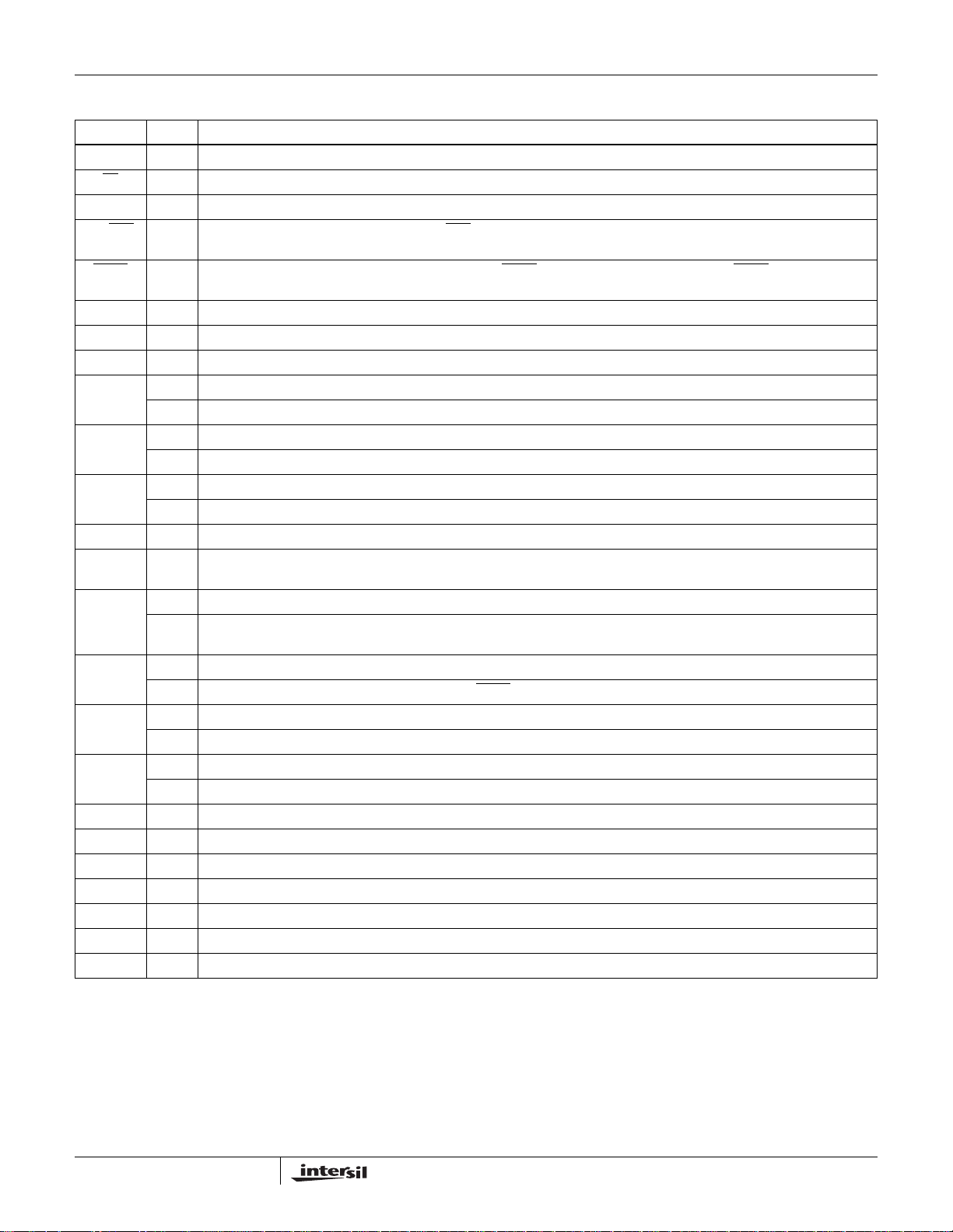
Pin Descriptions
PIN MODE FUNCTION
GND BOTH Ground connection.
LB
BOTH Enables loopback mode when low. Internally pulled-high.
NC BOTH No Connection.
ON/OFF
RXEN
SEL BOTH Interface Mode Select input. High puts corresponding port in RS-485 Mode, while a low puts it in RS-232 Mode.
V
D
D
DE RS-485 Driver output enable. The driver outputs, Y and Z, are enabled by bringing DE high. They are high impedance when DE is
R
R
SP RS-485 Speed control. Internally pulled-high. (QFN only)
C1+ RS-232 External capacitor (voltage doubler) is connected to this lead. Not needed if both ports in RS-485 Mode.
C1- RS-232 External capacitor (voltage doubler) is connected to this lead. Not needed if both ports in RS-485 Mode.
C2+ RS-232 External capacitor (voltage inverter) is connected to this lead. Not needed if both ports in RS-485 Mode.
C2- RS-232 External capacitor (voltage inverter) is connected to this lead. Not needed if both ports in RS-485 Mode.
V+ RS-232 Internally generated positive RS-232 transmitter supply (+5.5V). C3 not needed if both ports in RS-485 Mode.
BOTH If either port is in RS-232 mode, a low on ON/OFF disables the charge pumps. In either mode, a low disables all the outputs,
and places the device in low power shutdown. Internally pulled-high. ON = 1 for normal operation.
BOTH Active low receiver output enable. Rx is enabled when RXEN is low; Rx is high impedance when RXEN is high. Internally
pulled low. (QFN only)
BOTH System power supply input (5V).
CC
V
BOTH Logic-Level Supply. All TTL/CMOS inputs and outputs are powered by this supply. (QFN only)
L
A RS-232 Receiver input with ±15kV ESD protection. A low on A forces R
high; A high on A forces RA low.
A
RS-485 Inverting receiver input with ±15kV ESD protection.
B RS-232 Receiver input with ±15kV ESD protection. A low on B forces R
high; A high on B forces RB low.
B
RS-485 Noninverting receiver input with ±15kV ESD protection.
RS-232 Driver input. A low on DY forces output Y high. Similarly, a high on DY forces output Y low.
Y
RS-485 Driver input. A low on D
RS-232 Driver input. A low on DZ forces output Z high. Similarly, a high on DZ forces output Z low.
Z
forces output Y high and output Z low. Similarly, a high on DY forces output Y low and output Z high.
Y
low. Internally pulled high when port selected for RS-485 mode.
RS-232 Receiver output.
A
RS-485 Receiver output: If B > A by at least -40mV, R
unconnected (floating) or shorted together (i.e., full fail-safe).
RS-232 Receiver output.
B
RS-485 Not used. Internally pulled-high, and unaffected by RXEN
is high; If B < A by -200mV or more, RA is low; RA = High if A and B are
A
.
Y RS-232 Driver output with ±15kV ESD protection.
RS-485 Inverting driver output with ±15kV ESD protection.
Z RS-232 Driver output with ±15kV ESD protection.
RS-485 Noninverting driver output with ±15kV ESD protection.
V- RS-232 Internally generated negative RS-232 transmitter supply (-5.5V). C4 not needed if both ports in RS-485 Mode.
5
FN6202.1
December 20, 2005
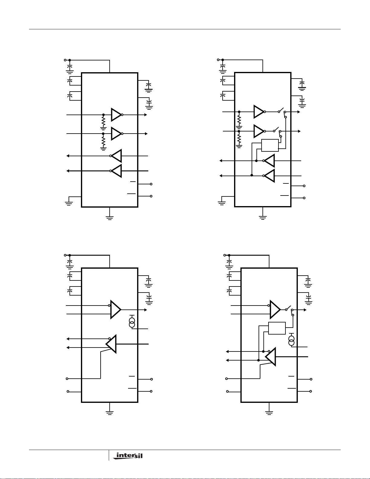
Typical Operating Circuit
RS-232 MODE WITHOUT LOOPBACK
ISL81334, ISL41334
RS-232 MODE WITH LOOPBACK
+5V
C
0.1µF
C
0.1µF
A1
B1
Y1
Z1
+
0.1µF
1
1
2
C1+
+
2
C1-
28
C2+
+
27
C2-
4
5kΩ
525
5kΩ
6
7
820
SEL1
26
V
CC
R
R
D
D
ON/OFF
V+
V-
LB
3
C
3
+
0.1µF
15
C
4
0.1µF
+
24
R
A1
R
B1
22
D
Y1
23
D
Z1
21
V
CC
V
CC
GND
14
NOTE: PINOUT FOR SOIC AND SSOP
SAME FOR PORT 2.
+5V
C
0.1µF
C
0.1µF
Y1
Z1
+
A1
0.1µF
1
1
2
C1+
+
2
C1-
28
C2+
+
27
C2-
4
26
V
CC
R
5kΩ
5
B1
5kΩ
R
LB
Rx
6
7
8
SEL1
GND
14
NOTE: PINOUT FOR SOIC AND SSOP
SAME FOR PORT 2.
D
D
ON/OFF
V+
V-
LB
3
C
3
+
0.1µF
15
C
4
0.1µF
+
24
R
A1
25
R
B1
22
D
Y1
23
D
Z1
21
GND
20
V
CC
RS-485 MODE WITHOUT LOOPBACK
+5V
+
C
0.1µF
C
0.1µF
A1
B1
Y1
Z1
V
CC
V
CC
0.1µF
1
1
2
C1+
+
2
C1-
28
C2+
+
27
C2-
4
5
6
7
23
DE1
820
SEL1
V
CC
GND
26
R
D
ON/OFF
14
LB
V+
V-
RS-485 MODE WITH LOOPBACK
+5V
+
0.1µF
1
3
C
3
+
0.1µF
15
C
4
0.1µF
+
24
R
A1
25
R
B1
22
D
Y1
C
0.1µF
C
0.1µF
1
2
A1
B1
Y1
Z1
21
V
CC
V
CC
V
CC
V
CC
C1+
+
2
C1-
28
C2+
+
27
C2-
4
5
6
7
DE1
23
820
SEL1
V
CC
GND
26
R
LB
Rx
D
14
V+
V-
LB
ON/OFF
3
C
3
+
0.1µF
15
C
4
0.1µF
+
24
R
A1
25
R
B1
22
D
Y1
21
GND
V
CC
NOTE: PINOUT FOR SOIC AND SSOP
SAME FOR PORT 2.
6
NOTE: PINOUT FOR SOIC AND SSOP
SAME FOR PORT 2.
FN6202.1
December 20, 2005
ISL81334, ISL41334
Absolute Maximum Ratings (T
VCC to Ground. . . . . . . . . . . . . . . . . . . . . . . . . . . . . . . . . . . . . . . 7V
V
(QFN Only) . . . . . . . . . . . . . . . . . . . . . . . . . -0.5V to VCC + 0.5V
L
Input Voltages
All Except A, B (non-QFN Package) . . . . . -0.5V to (V
All Except A, B (QFN Package) . . . . . . . . . . -0.5V to (V
Input/Output Voltages
A, B (Any Mode) . . . . . . . . . . . . . . . . . . . . . . . . . . . . -25V to +25V
Y, Z (Any Mode, Note 3) . . . . . . . . . . . . . . . . . . . -12.5V to +12.5V
R
, RB (non-QFN Package). . . . . . . . . . . . -0.5V to (VCC + 0.5V)
A
R
, RB (QFN Package) . . . . . . . . . . . . . . . . -0.5V to (VL + 0.5V)
A
Output Short Circuit Duration
Y, Z , R
, RB . . . . . . . . . . . . . . . . . . . . . . . . . . . . . . . . . . Indefinite
A
= 25°C) Thermal Information
A
Thermal Resistance (Typical, Note 4)
28 Ld SOIC Package . . . . . . . . . . . . . . . . . . . . . . . . 65
28 Ld SSOP Package . . . . . . . . . . . . . . . . . . . . . . . 60
CC
L
+ 0.5V)
+ 0.5V)
40 Ld QFN Package. . . . . . . . . . . . . . . . . . . . . . . . . 32
Maximum Junction Temperature (Plastic Package) . . . . . . . 150°C
Maximum Storage Temperature Range . . . . . . . . . . . -65°C to 150°C
Maximum Lead Temperature (Soldering 10s) . . . . . . . . . . . . 300°C
(SOIC and SSOP - Lead Tips Only)
Operating Conditions
Temperature Range . . . . . . . . . . . . . . . . . . . . . . . . . . . -40°C to 85°C
θ
JA
(°C/W)
ESD Rating . . . . . . . . . . . . . . . . . . . . . . . . . See Specification Table
CAUTION: Stresses above those listed in “Absolute Maximum Ratings” may cause permanent damage to the device. This is a stress only rating and operation of the
device at these or any other conditions above those indicated in the operational sections of this specification is not implied.
NOTES:
3. One output at a time, I
4. QFN θ
θ
is measured in free air with the component mounted on a high effective thermal conductivity test board with “direct attach” features.
JA
for other packages is measured with the component mounted on a high effective thermal conductivity test board in free air. See Tec h B ri e f
JA
≤ 100mA for ≤ 10 mins.
OUT
TB379 and Tech Brief TB389 for details.
Electrical Specifications Test Conditions: V
Typicals are at V
= 4.5V to 5.5V, C1 - C4 = 0.1µF, VL = VCC (for QFN only); Unless Otherwise Specified.
CC
= 5V, TA = 25°C (Note 5)
CC
TEMP
PARAMETER SYMBOL TEST CONDITIONS
DC CHARACTERISTICS - RS-485 DRIVER (SEL = V
Driver Differential V
Driver Differential V
(no load) V
OUT
(with load) V
OUT
OD1
OD2
R = 50Ω (RS-422) (Figure 1) Full 2.5 3.1 - V
CC
)
(°C) MIN TYP MAX UNITS
Full - - V
CC
V
R = 27Ω (RS-485) (Figure 1) Full 2.2 2.7 5 V
Change in Magnitude of Driver
Differential V
Complementary Output States
Driver Common-Mode V
OUT
for
OUT
Change in Magnitude of Driver
Common-Mode V
OUT
for
V
∆V
V
∆V
OD3
RD = 60Ω, R = 375Ω, VCM = -7V to 12V (Figure 1) Full 2 2.7 5 V
R = 27Ω or 50Ω (Figure 1) Full - 0.01 0.2 V
OD
R = 27Ω or 50Ω (Figure 1) (Note 9) Full - - 3.1 V
OC
R = 27Ω or 50Ω (Figure 1) (Note 9) Full - 0.01 0.2 V
OC
Complementary Output States
Driver Short-Circuit Current,
V
= High or Low
OUT
Driver Three-State Output
Leakage Current (Y, Z)
I
I
OS
-7V ≤ (VY or VZ) ≤ 12V (Note 7) Full 35 - 250 mA
OZ
Outputs Disabled,
V
= 0V or 5.5V
CC
= 12V Full - - 500 µA
V
OUT
= -7V Full -200 - - µA
V
OUT
DC CHARACTERISTICS - RS-232 DRIVER (SEL = GND)
Driver Output Voltage Swing V
Driver Output Short-Circuit Current I
OS
All T
O
V
Loaded with 3kΩ to Ground Full ±5.0 +6/-7 - V
OUTS
= 0V Full -60 25/-35 60 mA
OUT
DC CHARACTERISTICS - LOGIC PINS (i.e., DRIVER AND CONTROL INPUT PINS)
Input High Voltage V
V
V
VL = VCC if QFN Full 2 1.6 - V
IH1
VL = 3.3V (QFN Only) Full 2 1.2 - V
IH2
VL = 2.5V (QFN Only) Full 1.5 1 - V
IH3
7
FN6202.1
December 20, 2005
ISL81334, ISL41334
Electrical Specifications Test Conditions: V
Typicals are at V
= 4.5V to 5.5V, C1 - C4 = 0.1µF, VL = VCC (for QFN only); Unless Otherwise Specified.
CC
= 5V, TA = 25°C (Note 5) (Continued)
CC
TEMP
PARAMETER SYMBOL TEST CONDITIONS
Input Low Voltage V
Input Current I
V
V
IN1
I
IN2
VL = VCC if QFN Full - 1.4 0.8 V
IL1
VL = 3.3V (QFN Only) Full - 1 0.7 V
IL2
VL = 2.5V (QFN Only) Full - - 0.5 V
IL3
Pins Without Pull-ups or Pull-downs Full -2 - 2 µA
LB, ON/OFF, DE, SP (QFN), RXEN (QFN) Full -25 - 25 µA
DC CHARACTERISTICS - RS-485 RECEIVER INPUTS (SEL = V
Receiver Differential Threshold
Voltage
Receiver Input Hysteresis ∆V
Receiver Input Current (A, B) I
V
-7V ≤ VCM ≤ 12V, Full Failsafe Full -0.2 - -0.04 V
TH
VCM = 0V 25 - 35 - mV
TH
VCC = 0V or 4.5 to 5.5V VIN = 12V Full - - 0.8 mA
IN
CC
)
(°C) MIN TYP MAX UNITS
VIN = -7V Full -0.64 - - mA
Receiver Input Resistance R
-7V ≤ VCM ≤ 12V, VCC = 0 (Note 8) or
IN
4.5V ≤ V
CC
≤ 5.5V
Full 15 - - kΩ
DC CHARACTERISTICS - RS-232 RECEIVER INPUTS (SEL = GND)
Receiver Input Voltage Range V
Receiver Input Threshold V
Receiver Input Hysteresis ∆V
Receiver Input Resistance R
IN
IL
V
IH
TH
VIN = ±15V, VCC Powered Up (Note 8) Full 3 5 7 kΩ
IN
Full -25 - 25 V
Full - 1.4 0.8 V
Full 2.4 1.9 - V
25 - 0.5 - V
DC CHARACTERISTICS - RECEIVER OUTPUTS (485 OR 232 MODE)
Receiver Output High Voltage V
Receiver Output Low Voltage V
Receiver Short-Circuit Current I
Receiver Three-State Output
Current
Unused Receiver (R
) Pull-Up
B
OH1IO
V
OH2IO
V
OH3IO
OL
OSR
I
OZR
R
OBZ
= -2mA (VL = VCC if QFN) Full 3.5 4.6 - V
= -650µA, VL = 3V, QFN Only Full 2.6 2.9 - V
= -500µA, VL = 2.5V, QFN Only Full 2 2.4 - V
IO = 3mA Full - 0.1 0.4 V
0V ≤ VO ≤ V
CC
Full 7 - 85 mA
Output Disabled, 0V ≤ VO ≤ VCC (or VL for QFN) Full - - ±10 µA
ON/OFF = VCC, SELX = VCC (RS-485 Mode) 25 - 40 - kΩ
Resistance
POWER SUPPLY CHARACTERISTICS
No-Load Supply Current, Note 6 I
Shutdown Supply Current I
CC232
I
CC485
SHDN232
I
SHDN485
SEL1 or SEL2 = GND, LB = ON/OFF = V
SEL 1 & 2 = LB = DE = ON/OFF = V
CC
CC
ON/OFF = SELX = GND, LB = VCC, (SPX = V
if QFN)
ON/OFF = DEX = GND, SELX =
LB
= VCC, (SPX = GND if QFN)
SOIC/SSOP Full - 42 80 µA
QFN Full - 80 160 µA
Full - 3.7 7 mA
Full - 1.6 5 mA
Full - 25 50 µA
CC
ESD CHARACTERISTICS
Bus Pins (A, B, Y, Z) Any Mode Human Body Model 25 - 15 - kV
All Other Pins Human Body Model 25 - 4 - kV
8
FN6202.1
December 20, 2005
ISL81334, ISL41334
Electrical Specifications Test Conditions: V
Typicals are at V
= 4.5V to 5.5V, C1 - C4 = 0.1µF, VL = VCC (for QFN only); Unless Otherwise Specified.
CC
= 5V, TA = 25°C (Note 5) (Continued)
CC
TEMP
PARAMETER SYMBOL TEST CONDITIONS
(°C) MIN TYP MAX UNITS
RS-232 DRIVER AND RECEIVER SWITCHING CHARACTERISTICS (SEL = GND, ALL VERSIONS AND SPEEDS)
Driver Output Transition Region
SR R
Slew Rate
Driver Output Transition Time t
Driver Propagation Delay t
Driver Propagation Delay Skew t
Driver Enable Time from Shutdown t
DPHL
t
DPLH
DSKEWtDPHL
DENSDVOUT
Driver Maximum Data Rate DR
=3kΩ, Measured From
L
3V to -3V or -3V to 3V
, t
r
RL=3kΩ, CL = 2500pF, 10% - 90% Full 0.22 1.2 3.1 µs
f
RL=3kΩ, C
= 1000pF (Figure 6) Full - 1 2 µs
L
- t
(Figure 6) Full - 240 400 ns
DPLH
= ±3.0V 25 - 20 - µs
RL=3kΩ, CL= 1000pF, One Transmitter
D
CL ≥ 15pF Full - 18 30 V/µs
C
≤ 2500pF Full 4 12 - V/µs
L
Full - 1.2 2 µs
Full 460 650 - kbps
Switching per port
Receiver Propagation Delay t
Receiver Propagation Delay Skew t
RPHL
t
RPLH
RSKEWtRPHL
Receiver Maximum Data Rate DR
RS-485 DRIVER SWITCHING CHARACTERISTICS (FAST DATA RATE (20Mbps), SEL = V
Driver Differential Input to Output
t
DLH
C
= 15pF (Figure 7) Full - 50 120 ns
L
Full - 40 120 ns
- t
(Figure 7) Full - 10 40 ns
RPLH
CL= 15pF Full 0.46 2 - Mbps
R
, ALL VERSIONS (SPA = VCC if QFN))
CC
, t
DHLRDIFF
= 54Ω, CL = 100pF (Figure 2) Full 15 30 50 ns
Delay
Driver Output Skew t
Driver Differential Rise or Fall Time t
SKEW
R
Driver Enable to Output Low t
Driver Enable to Output High t
Driver Disable from Output Low t
Driver Disable from Output High t
Driver Enable from Shutdown to
Output Low
Driver Enable from Shutdown to
Output High
Driver Maximum Data Rate f
t
ZL(SHDN)RL
t
ZH(SHDN)RL
MAX
RS-485 DRIVER SWITCHING CHARACTERISTICS (MEDIUM DATA RATE (460kbps, QFN ONLY), SEL = V
Driver Differential Input to Output
Delay
Driver Output Skew t
Driver Differential Rise or Fall Time t
t
DLH
SKEW
R
Driver Enable to Output Low t
Driver Enable to Output High t
Driver Disable from Output Low t
Driver Disable from Output High t
Driver Enable from Shutdown to
Output Low
Driver Enable from Shutdown to
t
ZL(SHDN)RL
t
ZH(SHDN)RL
R
= 54Ω, CL = 100pF (Figure 2) Full - 0.5 10 ns
DIFF
, t
R
F
ZL
ZH
LZ
HZ
= 54Ω, CL = 100pF, Figure 2 Full 3 11 20 ns
DIFF
CL = 100pF, SW = VCC (Figure 3) Full - 27 60 ns
CL = 100pF, SW = GND (Figure 3) Full - 24 60 ns
CL = 15pF, SW = VCC (Figure 3) Full - 31 60 ns
CL = 15pF, SW = GND (Figure 3) Full - 24 60 ns
= 500Ω, CL = 100pF, SW = VCC (Figure 3) Full - 65 250 ns
= 500Ω, CL = 100pF, SW = GND (Figure 3) Full - 152 250 ns
R
= 54Ω, CL = 100pF (Figure 2) Full - 30 - Mbps
DIFF
, SPA = SPB= GND)
CC
, t
DHLRDIFF
, t
F
ZL
ZH
LZ
HZ
= 54Ω, CL = 100pF (Figure 2) Full 200 490 1000 ns
R
= 54Ω, CL = 100pF (Figure 2) Full - 110 400 ns
DIFF
R
= 54Ω, CL = 100pF (Figure 2) Full 300 600 1100 ns
DIFF
CL = 100pF, SW = VCC (Figure 3) Full - 30 300 ns
CL = 100pF, SW = GND (Figure 3) Full - 128 300 ns
CL = 15pF, SW = VCC (Figure 3) Full - 31 60 ns
CL = 15pF, SW = GND (Figure 3) Full - 24 60 ns
= 500Ω, CL = 100pF, SW = VCC (Figure 3) Full - 65 500 ns
= 500Ω, CL = 100pF, SW = GND (Figure 3) Full - 255 500 ns
Output High
9
FN6202.1
December 20, 2005

ISL81334, ISL41334
Electrical Specifications Test Conditions: V
Typicals are at V
= 4.5V to 5.5V, C1 - C4 = 0.1µF, VL = VCC (for QFN only); Unless Otherwise Specified.
CC
= 5V, TA = 25°C (Note 5) (Continued)
CC
TEMP
PARAMETER SYMBOL TEST CONDITIONS
Driver Maximum Data Rate f
MAX
R
= 54Ω, CL = 100pF (Figure 2) Full - 2000 - kbps
DIFF
RS-485 DRIVER SWITCHING CHARACTERISTICS (SLOW DATA RATE (115kbps, QFN ONLY), SEL = V
Driver Differential Input to Output
t
DLH
, t
DHLRDIFF
= 54Ω, CL = 100pF (Figure 2) Full 800 1500 2500 ns
(°C) MIN TYP MAX UNITS
, SPA = GND, SPB= VCC)
CC
Delay
Driver Output Skew t
Driver Differential Rise or Fall Time t
SKEW
R
Driver Enable to Output Low t
Driver Enable to Output High t
Driver Disable from Output Low t
Driver Disable from Output High t
Driver Enable from Shutdown to
Output Low
Driver Enable from Shutdown to
Output High
Driver Maximum Data Rate f
t
ZL(SHDN)RL
t
ZH(SHDN)RL
MAX
RS-485 RECEIVER SWITCHING CHARACTERISTICS (SEL = V
Receiver Input to Output Delay t
Receiver Skew | t
PLH
- t
|t
PHL
Receiver Maximum Data Rate f
PLH
SKEW
MAX
R
= 54Ω, CL = 100pF (Figure 2) Full - 350 1250 ns
DIFF
, t
R
F
ZL
ZH
LZ
HZ
= 54Ω, CL = 100pF (Figure 2) Full 1000 2000 3100 ns
DIFF
CL = 100pF, SW = VCC (Figure 3) Full - 32 600 ns
CL = 100pF, SW = GND (Figure 3) Full - 300 600 ns
CL = 15pF, SW = VCC (Figure 3) Full - 31 60 ns
CL = 15pF, SW = GND (Figure 3) Full - 24 60 ns
= 500Ω, CL = 100pF, SW = VCC (Figure 3) Full - 65 800 ns
= 500Ω, CL = 100pF, SW = GND (Figure 3) Full - 420 800 ns
R
= 54Ω, CL = 100pF (Figure 2) Full - 800 - kbps
DIFF
, ALL VERSIONS AND SPEEDS)
CC
, t
(Figure 4) Full 20 50 90 ns
PHL
(Figure 4) Full - 0.1 10 ns
Full - 40 - Mbps
RECEIVER ENABLE/DISABLE CHARACTERISTICS (ALL MODES AND SPEEDS)
Receiver Enable to Output Low t
Receiver Enable to Output High t
Receiver Disable from Output Low t
Receiver Disable from Output High t
Receiver Enable from Shutdown to
t
ZLSHDNCL
Output Low
Receiver Enable from Shutdown to
Output High
t
ZHSHDNCL
QFN Only, CL = 15pF, SW = VCC (Figure 5) Full - 22 60 ns
ZL
QFN Only, CL = 15pF, SW = GND (Figure 5) Full - 23 60 ns
ZH
QFN Only, CL = 15pF, SW = VCC (Figure 5) Full - 24 60 ns
LZ
QFN Only, CL = 15pF, SW = GND (Figure 5) Full - 25 60 ns
HZ
= 15pF, SW = VCC (Figure 5) RS-485 Mode Full - 260 700 ns
RS-232 Mode 25 - 35 - ns
= 15pF, SW = GND (Figure 5) RS-485 Mode Full - 260 700 ns
RS-232 Mode 25 - 25 - ns
NOTES:
5. All currents into device pins are positive; all currents out of device pins are negative. All voltages are referenced to device ground unless
otherwise specified.
6. Supply current specification is valid for loaded drivers when DE = 0V (RS-485 mode only).
7. Applies to peak current. See “Typical Performance Curves” for more information.
defaults to RS-485 mode (>15kΩ) when the device is unpowered (VCC = 0V), regardless of the state of the SEL inputs.
8. R
IN
≤ 5.25V.
9. V
CC
10
FN6202.1
December 20, 2005

Test Circuits and Waveforms
ISL81334, ISL41334
V
CC
SIGNAL
GENERATOR
DE
D
DE
V
CC
D
Y
Y
V
D
R
OD
D
Z
R
R
V
OC
FIGURE 1. RS-485 DRIVER VOD AND VOC TEST CIRCUIT
D
Y
CL = 100pF
Y
Y
R
D
Z
DIFF
= 100pF
C
L
OUT (Z)
OUT (Y)
DIFF OUT (Z - Y)
t
PLH
50% 50%
t
PHL
50% 50%
t
DLH
90% 90%
10% 10%
t
R
0V 0V
t
t
t
1.5V1.5V
PHL
PLH
DHL
3V
0V
V
OH
V
OL
V
OH
V
OL
+V
OD
-V
OD
t
F
SKEW = |t
FIGURE 2A. TEST CIRCUIT
(Y or Z) - t
PLH
PHL
(Z or Y)|
FIGURE 2B. MEASUREMENT POINTS
FIGURE 2. RS-485 DRIVER PROPAGATION DELAY AND DIFFERENTIAL TRANSITION TIMES
11
FN6202.1
December 20, 2005

ISL81334, ISL41334
Test Circuits and Waveforms (Continued)
DE
DY
SIGNAL
GENERATOR
FOR SHDN TESTS, SWITCH ON/OFF
Y
D
Z
RATHER THAN DE
PARAMETER ON/DE OUTPUT DY SW CL (pF)
t
HZ
t
LZ
t
ZH
t
ZL
t
ZH(SHDN)
t
ZL(SHDN)
1/- Y/Z 0/1 GND 15
1/- Y/Z 1/0 V
1/- Y/Z 0/1 GND 100
1/- Y/Z 1/0 V
-/1 Y/Z 0/1 GND 100
-/1 Y/Z 1/0 V
FIGURE 3A. TEST CIRCUIT
500Ω
SW
C
L
CC
CC
CC
100
100
FIGURE 3. RS-485 DRIVER ENABLE AND DISABLE TIMES
V
GND
15
CC
DE
(ON/OFF FOR SHDN)
t
ZH
t
ZH(SHDN)
OUT (Y, Z)
t
ZL
t
ZL(SHDN)
OUT (Y, Z)
FIGURE 3B. MEASUREMENT POINTS
ENABLED
OUTPUT HIGH
2.3V
2.3V
OUTPUT LOW
1.5V1.5V
t
HZ
t
LZ
3V
0V
VOH - 0.5V
VOL + 0.5V
V
OH
0V
V
CC
V
OL
0V
SIGNAL
GENERATOR
RXEN (QFN ONLY)
A
B
R
A
R
15pF
FIGURE 4A. TEST CIRCUIT
FIGURE 4. RS-485 RECEIVER PROPAGATION DELAY
RXEN (QFN ONLY)
A
SIGNAL
GENERATOR
FOR SHDN TESTS, SWITCH ON/OFF
R
B
R
A
RATHER THAN RXEN
1kΩ
15pF
SW
V
GND
PARAMETER ON/RXEN BSW
(QFN Only) 1/- +1.5V GND
t
HZ
(QFN Only) 1/- -1.5V V
t
LZ
CC
tZH (QFN Only) 1/- +1.5V GND
(QFN Only) 1/- -1.5V V
t
ZL
t
ZH(SHDN)
t
ZL(SHDN)
-/0 +1.5V GND
-/0 -1.5V V
CC
CC
CC
B
R
A
FIGURE 4B. MEASUREMENT POINTS
ON/OFF
(FOR SHDN TESTS)
RXEN (QFN ONLY)
t
ZH
t
ZH(SHDN)
R
A
t
ZL
t
ZL(SHDN)
R
A
t
PLH
1.5V 1.5V
1.5V
ENABLED
OUTPUT HIGH
1.5V
1.5V
OUTPUT LOW
t
t
HZ
t
0V0V
PHL
1.5V1.5V
LZ
+1.5V
-1.5V
3V
0V
3V
0V
VOH - 0.5V
VOL + 0.5V
V
CC
0V
V
OH
0V
V
CC
V
OL
FIGURE 5A. TEST CIRCUIT
FIGURE 5. RS-485 RECEIVER ENABLE AND DISABLE TIMES
12
FIGURE 5B. MEASUREMENT POINTS
FN6202.1
December 20, 2005

ISL81334, ISL41334
Test Circuits and Waveforms (Continued)
V
CC
SIGNAL
GENERATOR
SIGNAL
GENERATOR
DE
D
Y,Z
Y, Z
D
R
L
FIGURE 6A. TEST CIRCUIT
FIGURE 6. RS-232 DRIVER PROPAGATION DELAY AND TRANSITION TIMES
RXEN
A, B
R
A, RB
R
FIGURE 7A. TEST CIRCUIT
FIGURE 7. RS-232 RECEIVER PROPAGATION DELAY AND TRANSITION TIMES
C
L
CL = 15pF
D
Y,Z
OUT (Y,Z)
SKEW = |t
A, B
R
A, RB
SKEW = |t
1.5V1.5V
t
DPHL
0V 0V
- t
DPLH
|
DPHL
FIGURE 6B. MEASUREMENT POINTS
1.7V1.3V
t
RPLH
RPHL
- t
RPLH
t
RPHL
|
0.8V
FIGURE 7B. MEASUREMENT POINTS
2.4V
t
DPLH
3V
0V
3V
0V
V
O+
V
O-
V
OH
V
OL
13
FN6202.1
December 20, 2005

ISL81334, ISL41334
Typical Application
RS-232 to RS-485 Converter
The ISLX1334 are ideal for implementing a single IC 2-wire
(Tx Data, Rx Data) protocol converter, because each port can
be programmed for a different protocol. Figure 8 illustrates the
simple connections to create a single transceiver RS-232 to
RS-485 converter. Depending on the RS-232 data rate, using
an RS-422 bus as an RS-232 “extension cord” can extend the
transmission distance up to 4000’ (1220m). A similar circuit on
the other end of the cable completes the conversion to/from
RS-232.
+5V
+
0.1µF
0.1µF
NC
TxD
RS-232 IN
NC
RxD
RS-232 OUT
V
RS-485 IN
RS-485 OUT
0.1µF
1
C
C
CC
C1+
1
+
2
C1-
28
2
C2+
+
27
C2-
A1
4
B1
525
6
Y1
7
Z1
8
SEL1
9
SEL2
A2
13
12
B2
11
Y2
10
Z2
5kΩ
5kΩ
V
CC
GND
26
R
R
D
D
ON/OFF
R
D
14
V+
V-
R
A1
R
B1
D
Y1
D
Z1
R
A2
D
Y2
DE2
3
C
+
3
0.1µF
15
C
4
0.1µF
+
24
NC
22
23
20
V
CC
17
19
18
V
CC
Detailed Description
Each of the two ISLX1334 ports supports dual protocols:
RS-485/422, and RS-232. RS-485 and RS-422 are
differential (balanced) data transmission standards for use in
high speed (up to 20Mbps) networks, or long haul and noisy
environments. The differential signaling, coupled with
RS-485’s requirement for extended common mode range
(CMR) of +12V to -7V make these transceivers extremely
tolerant of ground potential differences, as well as voltages
induced in the cable by external fields. Both of these effects
are real concerns when communicating over the
RS-485/422 maximum distance of 4000’ (1220m). It is
important to note that the ISLX1334 don’t follow the RS-485
convention whereby the inverting I/O is labeled “B/Z”, and
the noninverting I/O is “A/Y”. Thus, in the application
diagrams below the 1334 A/Y (B/Z) pins connect to the B/Z
(A/Y) pins of the generic RS-485/422 ICs.
RS-422 is typically a point-to-point (one driver talking to one
receiver on a bus), or a point-to-multipoint (multidrop)
standard that allows only one driver and up to 10 receivers
on each bus. Because of the one driver per bus limitation,
RS-422 networks use a two bus, full duplex structure for
bidirectional communication, and the Rx inputs and Tx
outputs (no tri-state required) connect to different busses, as
shown in Figure 10.
Conversely, RS-485 is a true multipoint standard, which
allows up to 32 devices (any combination of drivers- must be
tri-statable - and receivers) on each bus. Now bidirectional
communication takes place on a single bus, so the Rx inputs
and Tx outputs of a port connect to the same bus lines, as
shown in Figure 9. Each port set to RS-485 /422 mode
includes one Rx and one Tx.
NOTE: PINOUT FOR SOIC AND SSOP
FIGURE 8. SINGLE IC RS-232 TO RS-485 CONVERTER
GENERIC 1/2 DUPLEX 485 XCVR
+
Tx/Rx
ISLX1334
RA
*
RXEN
DE
DY
* QFN ONLY
+5V
V
CC
B
R
A
Y
D
Z
GND
+
R
0.1µF
T
0.1µF
+5V
V
FIGURE 9. TYPICAL HALF DUPLEX RS-485 NETWORK
14
RO RE
R
CC
DE DI
D
B/Z
A/Y
GND
GENERIC 1/2 DUPLEX 485 XCVR
+
0.1µF
R
T
A/Y
B/Z
+5V
V
CC
GND
R
December 20, 2005
D
RO
RE
DE
DI
FN6202.1

ISLX1334 (MASTER)
1kΩ
OR NC
DY
DE
D
+5V
V
CC
ISL81334, ISL41334
GENERIC 422 Rx (SLAVE)
+
RO RE
0.1µF
+
0.1µF
Z
Y
+5V
R
V
CC
B
GND
A
GENERIC FULL DUPLEX 422 XCVR (SLAVE)
+5V
+
0.1µF
V
R
T
CC
A
B
RO
R
R
T
FIGURE 10. TYPICAL RS-422 NETWORK
RA
A
R
B
GND
RS-232 is a point-to-point, singled ended (signal voltages
referenced to GND) communication protocol targeting fairly
short (<150’, 46m) and low data rate (<1Mbps) applications.
Each port contains two transceivers (2 Tx and 2 Rx) in
RS-232 mode.
Protocol selection is handled via a logic pin (SELX) for each
port.
.
ISLX1334 Advantages
These dual protocol ICs offer many parametric
improvements versus those offered on competing dual
protocol devices. Some of the major improvements are:
15kV Bus Pin ESD - Eases board level requirements;
2.7V Diff V
- Better Noise immunity and/or distance;
OUT
Full Failsafe RS-485 Rx - Eliminates bus biasing;
Selectable RS-485 Data Rate - Up to 20Mbps, or slew
rate limited for low EMI and fewer termination issues;
High RS-232 Data Rate - >460kbps
Lower Tx and Rx Skews - Wider, consistent bit widths;
Lower I
- Max ICC is 2-4X lower than competition;
CC
Flow-Thru Pinouts - Tx, Rx bus pins on one side/logic
pins on the other, for easy routing to connector/UART;
Smaller (SSOP and QFN) and Pb-free Packaging.
RS-232 Mode
Rx Features
RS-232 receivers invert and convert RS-232 input levels
(±3V to ±25V) to the standard TTL/CMOS levels required by
a UART, ASIC, or µcontroller serial port. Receivers are
designed to operate at faster data rates than the drivers, and
they feature very low skews (10ns) so the receivers
contribute negligibly to bit width distortion. Inputs include the
standards required 3kΩ to 7kΩ pulldown resistor, so unused
inputs may be left unconnected. Rx inputs also have built-in
hysteresis to increase noise immunity, and to decrease
erroneous triggering due to slowly transitioning input signals.
Z
Y
GND
DI
D
Rx outputs are short circuit protected, and are only tristatable when the entire IC is shutdown via the ON/OFF
or via the active low RXEN
pin available on the QFN
pin,
package option (see “ISL41334 Special Features” for more
details).
Tx Features
RS-232 drivers invert and convert the standard TTL/CMOS
levels from a UART, or µcontroller serial port to RS-232
compliant levels (±5V minimum). The Tx delivers these
compliant output levels even at data rates of 650kbps, and
with loads of 1000pF. The drivers are designed for low skew
(typically 12% of the 500kbps bit width), and are compliant to
the RS-232 slew rate spec (4 to 30V/µs) for a wide range of
load capacitances. Tx inputs float if left unconnected, and
may cause I
increases. For the best results, connect
CC
unused inputs to GND.
Tx outputs are short circuit protected, and incorporate a
thermal SHDN feature to protect the IC in situations of
severe power dissipation. See the RS-485 section for more
details. Drivers tri-state only in SHDN, or when the 5V power
supply is off. The SHDN function is useful for tri-stating the
outputs if both ports will always be tri-stated together (e.g.,
used as a four transceiver RS-232 port), and if it is
acceptable for the Rx to be disabled as well. A single port Tx
disable can be accomplished by switching the port to
RS-485 mode, and then using the corresponding DE pin to
tri-state the drivers. Of course, the Rx is now an RS-485 Rx,
so this option is feasible only if the Rx aren’t needed when
the Tx are disabled.
Charge Pumps
The on-chip charge pumps create the RS-232 transmitter
power supplies (typically +6/-7V) from a single supply as low
as 4.5V, and are enabled only if either port is configured for
RS-232 operation. The efficient design requires only four
15
FN6202.1
December 20, 2005

ISL81334, ISL41334
small 0.1µF capacitors for the voltage doubler and inverter
functions. By operating discontinuously (i.e., turning off as
soon as V+ and V- pump up to the nominal values), the
charge pump contribution to RS-232 mode I
is reduced
CC
significantly. Unlike competing devices that require the
charge pump in RS-485 mode, disabling the charge pump
saves power, and minimizes noise. If the application keeps
both ports in RS-485 mode (e.g., a dedicated dual channel
RS-485 interface), then the charge pump capacitors aren’t
even required.
Data Rates and Cabling
Drivers operate at data rates up to 650kbps, and are
guaranteed for data rates up to 460kbps. The charge pumps
and drivers are designed such that one driver in each port
can be operated at the rated load, and at 460kbps (see
Figure 34). Figure 34 also shows that drivers can easily drive
several thousands of picofarads at data rates up to 250kbps,
while still delivering compliant ±5V output levels.
Receivers operate at data rates up to 2Mbps. They are
designed for a higher data rate to facilitate faster factory
downloading of software into the final product, thereby
improving the user’s manufacturing throughput.
Figures 37 and 38 illustrate driver and receiver waveforms at
250kbps, and 500kbps, respectively. For these graphs, one
driver of each port drives the specified capacitive load, and a
receiver in the port.
RS-232 doesn’t require anything special for cabling; just a
single bus wire per transmitter and receiver, and another
wire for GND. So an ISLX1334 RS-232 port uses a five
conductor cable for interconnection. Bus terminations are
not required, nor allowed, by the RS-232 standard.
RS-485 Mode
Rx Features
RS-485 receivers convert differential input signals as small
as 200mV, as required by the RS-485 and RS-422
standards, to TTL/CMOS output levels. The differential Rx
provides maximum sensitivity, noise immunity, and common
mode rejection. Per the RS-485 standard, receiver inputs
function with common mode voltages as great as ±7V
outside the power supplies (i.e., +12V and -7V), making
them ideal for long networks where induced voltages are a
realistic concern. Each RS-485/422 port includes a single
receiver (RA), and the unused Rx output (RB) is disabled,
but pulled high by an internal current source. The internal
current source turns off in SHDN.
Worst case receiver input currents are 20% lower than the 1
“unit load” (1mA) RS-485 limit, which translates to a 15kΩ
minimum input resistance.
These receivers include a “full fail-safe” function that
guarantees a high level receiver output if the receiver inputs
are unconnected (floating), shorted together, or if the bus is
terminated but undriven (i.e., differential voltage collapses to
near zero due to termination). Failsafe with shorted, or
terminated and undriven inputs is accomplished by setting
the Rx upper switching point at -40mV, thereby ensuring that
the Rx recognizes a 0V differential as a high level.
All the Rx outputs are short circuit protected, and are tri-state
when the IC is forced into SHDN, but ISL81334 (SOIC and
SSOP) receiver outputs are not independently tri-statable.
ISL41334 (QFN) receiver outputs are tri-statable via an
active low RXEN
input for each port (see “ISL41334 Special
Features” for more details).
Tx Features
The RS-485/422 driver is a differential output device that
delivers at least 2.2V across a 54Ω load (RS-485), and at
least 2.5V across a 100Ω load (RS-422). Both levels
significantly exceed the standards requirements, and these
exceptional output voltages increase system noise immunity,
and/or allow for transmission over longer distances. The
drivers feature low propagation delay skew to maximize bit
widths, and to minimize EMI.
To allow multiple drivers on a bus, the RS-485 spec requires
that drivers survive worst case bus contentions undamaged.
The ISLX1334 drivers meet this requirement via driver
output short circuit current limits, and on-chip thermal
shutdown circuitry. The output stages incorporate current
limiting circuitry that ensures that the output current never
exceeds the RS-485 spec, even at the common mode
voltage range extremes. In the event of a major short circuit
condition, devices also include a thermal shutdown feature
that disables the drivers whenever the die temperature
becomes excessive. This eliminates the power dissipation,
allowing the die to cool. The drivers automatically re-enable
after the die temperature drops about 15 degrees. If the
contention persists, the thermal shutdown/re-enable cycle
repeats until the fault is cleared. Receivers stay operational
during thermal shutdown.
RS-485 multi-driver operation also requires drivers to include
tri-state functionality, so each port has a DE pin to control
this function. If the driver is used in an RS-422 network, such
that driver tri-state isn’t required, then the DE pin can be left
unconnected and an internal pull-up keeps it in the enabled
state. Drivers are also tri-stated when the IC is in SHDN, or
when the 5V power supply is off.
Speed Options
The ISL81334 (SOIC/SSOP) has fixed, high slew rate driver
outputs optimized for 20Mbps data rates. The ISL41334
(QFN) offers three user selectable data rate options: “Fast”
for high slew rate and 20Mbps; “Medium” with slew rate
limiting set for 460kbps; “Slow” with even more slew rate
limiting for 115kbps operation. See the “Data Rate“ and
“Slew Rate Limited Data Rates” sections for more
information.
Receiver performance is the same for all three speed
options.
16
FN6202.1
December 20, 2005

ISL81334, ISL41334
Data Rate, Cables, and Terminations
RS-485/422 are intended for network lengths up to 4000’
(1220m), but the maximum system data rate decreases as
the transmission length increases. Devices operating at the
maximum data rate of 20Mbps are limited to lengths of 2030’ (6-9m), while devices operating at or below 115kbps can
operate at the maximum length of 4000’ (1220m).
Higher data rates require faster edges, so both the
ISLX1334 versions offer an edge rate capable of 20Mbps
data rates. The ISL41334 also offers two slew rate limited
edge rates to minimize problems at slower data rates.
Nevertheless, for the best jitter performance when driving
long cables, the faster speed settings may be preferable,
even at low data rates. See the “RS-485 Slew Rate Limited
Data Rates” section for details.
Twisted pair is the cable of choice for RS-485/422 networks.
Twisted pair cables tend to pick up noise and other
electromagnetically induced voltages as common mode
signals, which are effectively rejected by the differential
receivers in these ICs.
The preferred cable connection technique is “daisychaining”, where the cable runs from the connector of one
device directly to the connector of the next device, such that
cable stub lengths are negligible. A “backbone” structure,
where stubs run from the main backbone cable to each
device’s connector, is the next best choice, but care must be
taken to ensure that each stub is electrically “short”. See
Table 4 for recommended maximum stub lengths for each
speed option.
TABLE 4. RECOMMENDED STUB LENGTHS
SPEED OPTION
SLOW 350-500 (107-152)
MED 100-150 (30.5 - 46)
FAST 1-3 (0.3 - 0.9)
MAXIMUM STUB LENGTH
ft (m)
Proper termination is imperative to minimize reflections
when using the 20Mbps speed option. Short networks using
the medium and slow speed options need not be terminated,
but terminations are recommended unless power dissipation
is an overriding concern. Note that the RS-485 spec allows a
maximum of two terminations on a network, otherwise the Tx
output voltage may not meet the required V
OD
.
In point-to-point, or point-to-multipoint (RS-422) networks,
the main cable should be terminated in its characteristic
impedance (typically 120Ω) at the end farthest from the
driver. In multi-receiver applications, stubs connecting
receivers to the main cable should be kept as short as
possible, but definitely shorter than the limits shown in Table
4. Multipoint (RS-485) systems require that the main cable
be terminated in its characteristic impedance at both ends.
Again, keep stubs connecting a transceiver to the main
cable as short as possible, and refer to Table 4. Avoid “star”,
and other configurations, where there are many “ends”
which would require more than the two allowed terminations
to prevent reflections.
High ESD
All pins on the ISLX1334 include ESD protection structures
rated at ±4kV (HBM), which is good enough to survive ESD
events commonly seen during manufacturing. But the bus
pins (Tx outputs and Rx inputs) are particularly vulnerable to
ESD events because they connect to an exposed port on the
exterior of the finished product. Simply touching the port
pins, or connecting a cable, can destroy an unprotected port.
ISLX1334 bus pins are fitted with advanced structures that
deliver ESD protection in excess of ±15kV (HBM), without
interfering with any signal in the RS-485 or the RS-232
range. This high level of protection may eliminate the need
for board level protection, or at the very least will increase
the robustness of any board level scheme.
Small Packages
Many competing dual protocol ICs are available only in
monstrously large 24 to 28 Ld SOIC packages. The
ISL81334’s 28 Ld SSOP is 50% smaller than even a 24 Ld
SOIC, and the ISL41334’s tiny 6x6mm QFN is 80% smaller
than a 28 Ld SOIC.
Flow Through Pinouts
Even the ISLX1334 pinouts are features, in that the “flowthrough” design simplifies board layout. Having the bus pins
all on one side of the package for easy routing to a cable
connector, and the Rx outputs and Tx inputs on the other
side for easy connection to a UART, avoids costly and
problematic crossovers. Figure 11 illustrates the flowthrough nature of the pinout.
ISL81334
A1
B1
Y1
Z1
Z2
Y2
CONNECTOR
B2
A2
FIGURE 11. ILLUSTRATION OF FLOW THROUGH PINOUT
R
RA1
D
DY1
DY2
RA2
UART
OR
ASIC
OR
µCONTROLLER
Low Power Shutdown (SHDN) Mode
The ON/OFF pin is driven low to place the IC (both ports) in
the SHDN mode, and the already low supply current drops to
as low as 25µA. If this functionality isn’t desired, the pin can
be left disconnected (thanks to the internal pull-up), or it
should be connected to V
1kΩ resistor. SHDN disables the Tx and Rx outputs, and
(VL for the QFN), through a
CC
17
FN6202.1
December 20, 2005

ISL81334, ISL41334
disables the charge pumps if either port is in RS-232 mode,
so V+ collapses to V
, and V- collapses to GND.
CC
All but 5uA of SHDN ICC current is due to control input (ON,
LB
, SP, DE) pull-up resistors (~20µA/resistor), so SHDN ICC
varies depending on the ISLX1334 configuration. The spec
tables indicate the worst case values, but careful selection of
the configuration yields lower currents. For example, in RS232 mode the SP pins aren’t used, so if both ports are
configured for RS-232, floating or tying the SP pins high
minimizes SHDN I
. Likewise in RS-485 mode, the drivers
CC
are disabled in SHDN, so driving the DE pins high during this
time also reduces I
CC
.
On the ISL41334, the SHDN ICC increases as VL
decreases. V
rather than V
second stage input isn’t driven to the rail, so some I
powers the input stage and sets its VOH at VL
L
. VCC powers the second stage, but the
CC
CC
current flows. See Figure 21 for details.
When enabling from SHDN in RS-232 mode, allow at least
20µs for the charge pumps to stabilize before transmitting
data. The charge pumps aren’t used in RS-485 mode, so the
transceiver is ready to send or receive data in less than 1µs,
which is much faster than competing devices that require the
charge pump for all modes of operation.
Internal Loopback Mode
Driving the LB pin low places both ports in the loopback
mode, a mode that facilitates implementing board level self
test functions. In loopback, internal switches disconnect the
Rx inputs from the Rx outputs, and feed back the Tx outputs
to the appropriate Rx output. This way the data driven at the
Tx input appears at the corresponding Rx output (refer to
“Typical Operating Circuits”). The Tx outputs remain
connected to their terminals, so the external loads are
reflected in the loopback performance. This allows the
loopback function to potentially detect some common bus
faults such as one or both driver outputs shorted to GND, or
outputs shorted together.
Note that the loopback mode uses an additional set of
receivers, as shown in the “Typical Operating Circuits”.
These loopback receivers are not standards compliant, so
the loopback mode can’t be used to implement a half-duplex
RS-485 transceiver.
If loopback won’t be utilized, the pin can be left disconnected
(thanks to the internal pull-up), or it should be connected to
V
(VL for the QFN), through a 1kΩ resistor.
CC
ISL41334 (QFN Package) Special Features
Logic Supply (VL Pin)
The ISL41334 (QFN) includes a VL pin that powers the logic
inputs (Tx inputs and control pins) and Rx outputs. These
pins interface with “logic” devices such as UARTs, ASICs,
and µcontrollers, and today most of these devices use power
supplies significantly lower than 5V. Thus, a 5V output level
from a 5V powered dual protocol IC might seriously
overdrive and damage the logic device input. Similarly, the
the logic device’s low V
powered dual protocol input. Connecting the V
might not exceed the VIH of a 5V
OH
pin to the
L
power supply of the logic device - as shown in Figure 12 limits the ISL41334’s Rx output V
to VL (see Figure 15),
OH
and reduces the Tx and control input switching points to
values compatible with the logic device output levels.
Tailoring the logic pin input switching points and output levels
to the supply voltage of the UART, ASIC, or µcontroller
eliminates the need for a level shifter/translator between the
two ICs.
VCC = +5V
= 5V
V
OH
R
A
≥ 2V
V
IH
D
Y
GND
ISL81334
VCC = +5V
V
L
R
A
D
Y
GND
ISL41334
FIGURE 12. USING VL PIN TO ADJUST LOGIC LEVELS
V
can be anywhere from VCC down to 1.65V, but the input
L
V
V
OH
= 0.9V
IH
= 2V
V
OH
V
OH
VCC = +2V
R
XD
T
XD
≤ 2V
UART/PROCESSOR
VCC = +2V
R
XD
T
XD
≤ 2V
UART/PROCESSOR
ESD
DIODE
GND
ESD
DIODE
GND
switching points may not provide enough noise margin when
V
< 1.8V. Table 5 indicates typical VIH and VIL values for
L
various V
particular V
values so the user can ascertain whether or not a
L
voltage meets his needs.
L
TABLE 5. VIH AND VIL vs. VL FOR VCC = 5V
(V) VIH (V) VIL (V)
V
L
1.65V 0.79 0.50
1.8V 0.82 0.60
2.0V 0.87 0.69
2.5V 0.99 0.86
3.3V 1.19 1.05
18
FN6202.1
December 20, 2005

ISL81334, ISL41334
The VL supply current (IL) is typically less than 100µA, as
shown in Figures 20 and 21. All of the DC V
to inputs with internal pull-up resistors (DE, SP, LB
being driven to the low input state. The worst case I
occurs during SHDN (see Figure 20), due to the I
the ON/OFF
I
through an input pull-up resistor is ~20µA, so the IL in
IL
Figure 20 drops by about 40µA (at V
pin pull-up resistor when that pin is driven low.
L
SP inputs are high (middle vs. top curve). I
RS-232 mode, because only the ON/OFF
driven low. When all these inputs are driven high, I
current is due
L
, ON/OFF)
current
L
through
L
= 5V) when the two
is lowest in the
L
pin should be
drops to
L
<1µA, so to minimize power dissipation drive these inputs
high when unneeded (e.g., SP inputs aren’t used in RS-232
mode, so drive them high).
Active Low Rx Enable (RXEN)
In many RS-485 applications, especially half duplex
configurations, users like to accomplish “echo cancellation”
by disabling the corresponding receiver while its driver is
transmitting data. This function is available on the QFN
package via an active low RXEN
active low function also simplifies direction control, by
allowing a single Tx/Rx
direction control line. If an active high
RXEN were used, either two valuable I/O pins would be
used for direction control, or an external inverter is required
between DE and RXEN. Figure 13 details the advantage of
using the RXEN
Tx/Rx
ACTIVE HIGH RX ENABLE
Tx/Rx
pin.
RA
RXEN
DEN
DY
ISL41334
RA
RXEN
*
DE
DY
* QFN ONLY
pin for each port. The
+5V
ISL81387
V
CC
B
R
A
Y
D
Z
GND
+5V
V
CC
B
R
A
Y
D
Z
GND
+
+
0.1µF
0.1µF
RS-485 Slew Rate Limited Data Rates
The SOIC and SSOP versions of this IC operate with Tx
output transitions optimized for a 20Mbps data rate. These
fast edges may increase EMI and reflection issues, even
though fast transitions aren’t required at the lower data rates
used by many applications. The ISL41334 (QFN version)
solves this problem by offering two additional, slew rate
limited, data rates that are optimized for speeds of 115kbps,
and 460kbps.The slew limited edges permit longer
unterminated networks, or longer stubs off terminated
busses, and help minimize EMI and reflections.
Nevertheless, for the best jitter performance when driving
long cables, the faster speed options may be preferable,
even at lower data rates. The faster output transitions deliver
less variability (jitter) when loaded with the large capacitance
associated with long cables. Figures 43, 44, and 45 detail
the jitter performance of the three speed options while
driving three different cable lengths. The figures show that
under all conditions the faster the edge rate, the better the
jitter performance. Of course, faster transitions require more
attention to ensuring short stub lengths, and quality
terminations, so there are trade-offs to be made. Assuming a
jitter budget of 10%, it is likely better to go with the slow
speed option for data rates of 115kbps or less, to minimize
fast edge effects. Likewise, the medium speed option is a
good choice for data rates between 115kbps and 460kbps.
For higher data rates, or when the absolute best jitter is
required, use the high speed option.
Speed selection is via the SPA and SPB pins (see Table 3),
and the selection pertains to each port programmed for
RS-485 mode.
Evaluation Board
An evaluation board, part number ISL41334EVAL1, is
available to assist in assessing the dual protocol IC’s
performance. The evaluation board contains a QFN
packaged device, but because the same die is used in all
packages, the board is also useful for evaluating the
functionality of the other versions. The board’s design allows
for evaluation of all standard features, plus the QFN specific
features. Refer to the eval board application note for details,
and contact your sales rep for ordering information.
ACTIVE LOW RX ENABLE
FIGURE 13. USING ACTIVE LOW vs ACTIVE HIGH RX
ENABLE
19
FN6202.1
December 20, 2005

ISL81334, ISL41334
Typical Performance Curves V
50
40
30
20
10
RECEIVER OUTPUT CURRENT (mA)
0
012345
RECEIVER OUTPUT VOLTAGE (V)
V
OH
, 85°C
V
, 25°C
OH
= VL = 5V, TA = 25°C; Unless Otherwise Specified
CC
V
, 25°C
OL
V
, 85°C
OL
FIGURE 14. RECEIVER OUTPUT CURRENT vs RECEIVER
OUTPUT VOLTAGE
100
90
80
70
60
50
40
30
20
DRIVER OUTPUT CURRENT (mA)
10
0
012345
DIFFERENTIAL OUTPUT VOLTAGE (V)
FIGURE 16. RS-485, DRIVER OUTPUT CURRENT vs
DIFFERENTIAL OUTPUT VOLTAGE
5
4
3
IOH = -1mA
2
IOH = -8mA
1
HIGH OUTPUT VOLTAGE (V)
0
012345
VL (V)
IOH = -4mA
FIGURE 15. RECEIVER HIGH OUTPUT VOLTAGE vs LOGIC
SUPPLY VOLTAGE (V
3.6
3.5
3.4
3.3
3.2
3.1
DIFFERENTIAL OUTPUT VOLTAGE (V)
3
-40 0 50 85
-25 25 75
TEMPERATURE (°C)
R
DIFF
)
L
= 100Ω
R
DIFF
= 54Ω
FIGURE 17. RS-485, DRIVER DIFFERENTIAL OUTPUT
VOLTAGE vs TEMPERATURE
150
85°C
-40°C
Y OR Z = LOW
25°C
OUTPUT VOLTAGE (V)
100
50
0
-50
OUTPUT CURRENT (mA)
-100
-150
-7 -6 -4 -2 0 2 4 6 8 10 12
FULL TEMP RANGE
Y OR Z = HIGH
FIGURE 18. RS-485, DRIVER OUTPUT CURRENT vs SHORT
CIRCUIT VOLTAGE
20
4
3.5
3
2.5
(mA)
CC
I
2
1.5
1
-40 0 50 85
RS-232, RXEN = X
RS-485, HALF DUPLEX, DE = VCC, RXEN = X
RS-485, FULL DUPLEX, DE = VCC, RXEN = X
RS-485, DE = GND, RXEN = X
-25 25 75
TEMPERATURE (°C)
FIGURE 19. SUPPLY CURRENT vs TEMPERATURE
December 20, 2005
FN6202.1

ISL81334, ISL41334
Typical Performance Curves V
10m
NO LOAD
= VL or GND
V
IN
LB
= V
L
1m
(A)
L
I
RS-485, DE = ON = SP = GND
100µ
10µ
RS-485, DE = ON = GND, SP = V
1µ
23456
VL ≤ V
RS-232, ON = GND, SP = V
L
VL (V)
= VL = 5V, TA = 25°C; Unless Otherwise Specified (Continued)
CC
CCVL
> V
CC
L
FIGURE 20. RS-232, VL SUPPLY CURRENT vs VL VO LTA GE
(QFN ONLY)
1700
R
= 54Ω, CL = 100pF
DIFF
1650
1600
t
1550
1500
PROPAGATION DELAY (ns)
1450
DHL
t
DLH
t
DHL
600
500
RS-232/RS-485 I
400
(µA)
L
300
and I
CC
I
200
100
RS-485 I
L
0
22.533.544.55
FIGURE 21. V
and VL SHDN SUPPLY CURRENTS vs VL
CC
CC
VL (V)
NO LOAD
= VL or GND
V
IN
LB
= V
ON = DZ/DE = DY = GND
SP = GND
L
SP = VLRS-232 I
VOLTAGE (QFN ONLY)
400
R
= 54Ω, CL = 100pF
DIFF
350
300
250
200
SKEW (ns)
150
100
50
|t
PHLZ
- t
PLHY
|t
|
DLH
- t
|t
PLHZ
DHL
- t
|
PHLY
|
L
1400
-40 0 50 85
-25 25 75
TEMPERATURE (°C)
FIGURE 22. RS-485, DRIVER PROPAGATION DELAY vs
TEMPERATURE (SLOW DATA RATE, QFN ONLY)
21
-40 0 50 85
-25 25 75
TEMPERATURE (°C)
FIGURE 23. RS-485, DRIVER SKEW vs TEMPERATURE
(SLOW DATA RATE, QFN ONLY)
December 20, 2005
FN6202.1

ISL81334, ISL41334
Typical Performance Curves V
560
R
= 54Ω, CL = 100pF
DIFF
550
540
530
520
510
500
490
PROPAGATION DELAY (ns)
480
470
-40 0 50 85
t
DHL
-25 25 75
TEMPERATURE (°C)
= VL = 5V, TA = 25°C; Unless Otherwise Specified (Continued)
CC
t
DLH
t
DHL
FIGURE 24. RS-485, DRIVER PROPAGATION DELAY vs
TEMPERATURE (MEDIUM DATA RATE, QFN
ONLY)
40
R
= 54Ω, CL = 100pF
DIFF
35
t
DHL
30
t
DLH
25
PROPAGATION DELAY (ns)
120
R
= 54Ω, CL = 100pF
DIFF
100
|t
- t
PHLZ
80
60
SKEW (ns)
40
20
0
-40 0 50 85
|
PLHY
|t
- t
PLHZ
-25 25 75
|
PHLY
|t
- t
DLH
DHL
TEMPERATURE (°C)
|
FIGURE 25. RS-485, DRIVER SKEW vs TEMPERATURE
(MEDIUM DATA RATE, QFN ONLY)
2.5
R
= 54Ω, CL = 100pF
DIFF
2
|t
- t
|
DHL
|
1.5
1
SKEW (ns)
0.5
|t
PLHZ
- t
DLH
PHLY
20
-40 0 50 85
-25 25 75
TEMPERATURE (°C)
FIGURE 26. RS-485, DRIVER PROPAGATION DELAY vs
TEMPERATURE (FAST DATA RATE)
R
= 60Ω, CL = 100pF
D
Y
5
0
RECEIVER OUTPUT (V)
5
4
Y
3
2
Z
1
0
DRIVER OUTPUT (V)
DIFF
R
A
TIME (400ns/DIV)
5
0
FIGURE 28. RS-485, DRIVER AND RECEIVER WAVEFORMS,
LOW TO HIGH (SLOW DATA RATE, QFN ONLY)
|t
- t
PHLZ
0
-40 0 50 85
|
PLHY
-25 25 75
TEMPERATURE (°C)
FIGURE 27. RS-485, DRIVER SKEW vs TEMPERATURE
(FAST DATA RATE)
R
= 60Ω, CL = 100pF
DIFF
D
Y
DRIVER INPUT (V)
5
0
RECEIVER OUTPUT (V)
5
4
Z
3
2
Y
1
0
DRIVER OUTPUT (V)
R
A
TIME (400ns/DIV)
5
0
DRIVER INPUT (V)
FIGURE 29. RS-485, DRIVER AND RECEIVER WAVEFORMS,
HIGH TO LOW (SLOW DATA RATE, QFN ONLY)
22
FN6202.1
December 20, 2005

ISL81334, ISL41334
Typical Performance Curves V
R
= 60Ω, CL = 100pF
DIFF
D
Y
5
0
RECEIVER OUTPUT (V)
5
4
Y
3
2
Z
1
0
DRIVER OUTPUT (V)
R
A
TIME (200ns/DIV)
= VL = 5V, TA = 25°C; Unless Otherwise Specified (Continued)
CC
FIGURE 30. RS-485, DRIVER AND RECEIVER WAVEFORMS,
LOW TO HIGH (MEDIUM DATA RATE, QFN ONLY)
R
= 60Ω, CL = 100pF
DIFF
D
Y
5
0
RECEIVER OUTPUT (V)
5
4
Y
3
2
Z
1
0
DRIVER OUTPUT (V)
TIME (10ns/DIV)
R
A
5
0
DRIVER INPUT (V)
5
0
DRIVER INPUT (V)
R
= 60Ω, CL = 100pF
DIFF
D
Y
5
0
RECEIVER OUTPUT (V)
5
4
Z
3
2
Y
1
0
DRIVER OUTPUT (V)
R
A
TIME (200ns/DIV)
5
0
FIGURE 31. RS-485, DRIVER AND RECEIVER WAVEFORMS,
HIGH TO LOW (MEDIUM DATA RATE, QFN ONLY)
R
= 60Ω, CL = 100pF
DIFF
D
Y
5
0
RECEIVER OUTPUT (V)
5
4
Z
3
2
Y
1
0
DRIVER OUTPUT (V)
TIME (10ns/DIV)
R
A
5
0
DRIVER INPUT (V)
DRIVER INPUT (V)
FIGURE 32. RS-485, DRIVER AND RECEIVER WAVEFORMS,
LOW TO HIGH (FAST DATA RATE)
7.5
V
5
2.5
0
-2.5
-5
TRANSMITTER OUTPUT VOLTAGE (V)
-7.5
+
OUT
ALL T
1 TRANSMITTER/PORT AT 250kbps or 500kbps,
OTHER TRANSMITTERS AT 30kbps
V
OUT
LOADED WITH 3kΩ TO GND
OUTS
-
1000 2000 3000 4000 50000
LOAD CAPACITANCE (pF)
250kbps
500kbps
500kbps
250kbps
FIGURE 34. RS-232, TRANSMITTER OUTPUT VOLTAGE vs
LOAD CAPACITANCE
23
RS-232 REGION OF NONCOMPLIANCE
FIGURE 33. RS-485, DRIVER AND RECEIVER WAVEFORMS,
HIGH TO LOW (FAST DATA RATE)
7.5
5
2.5
OUTPUTS STATIC
ALL T
0
-2.5
-5
TRANSMITTER OUTPUT VOLTAGE (V)
-7.5
-40 0 50 85
LOADED WITH 3kΩ TO GND
OUTS
-25 25 75
TEMPERATURE (°C)
V
OUT
V
OUT
+
-
FIGURE 35. RS-232, TRANSMITTER OUTPUT VOLTAGE vs
TEMPERATURE
FN6202.1
December 20, 2005

ISL81334, ISL41334
Typical Performance Curves V
40
30
20
10
V
SHORTED TO GND
OUT
0
-10
-20
-30
TRANSMITTER OUTPUT CURRENT (mA)
-40
-40 0 50 85
-25 25 75
TEMPERATURE (°C)
Y or Z = LOW
Y or Z = HIGH
= VL = 5V, TA = 25°C; Unless Otherwise Specified (Continued)
CC
FIGURE 36. RS-232, TRANSMITTER SHORT CIRCUIT
CURRENT vs TEMPERATURE
CL = 1000pF, 1 CHANNEL SWITCHING/PORT
5
DY
0
5
0
Y/A
-5
5
RA
0
1µs/DIV.
FIGURE 38. RS-232, TRANSMITTER AND RECEIVER
WAVEFORMS AT 500kbps
CL = 3500pF, 1 CHANNEL SWITCHING/PORT
5
DY
0
5
0
Y/A
-5
5
RA
0
2µs/DIV.
FIGURE 37. RS-232, TRANSMITTER AND RECEIVER
WAVEFORMS AT 250kbps
60
58
56
54
52
50
RECEIVER + DUTY CYCLE (%)
48
50
FULL TEMP RANGE
SR IN = 15V/µs
SR IN = 100V/µs
500 1000 1500 2000
DATA RATE (kbps)
VIN = ±5V
FIGURE 39. RS-232, RECEIVER OUTPUT +DUTY CYCLE vs
DATA RATE
1100
1000
900
800
700
600
500
400
DATA RATE (kbps)
300
1 TRANSMITTER AT 85°C
200
100
100 1000 2000 3000 4000 5000
ALL T
2 TRANSMITTERS AT 85°C
LOAD CAPACITANCE (pF)
LOADED WITH 5kΩ TO GND
OUTS
2 TRANSMITTERS AT 25°C
1 TRANSMITTER AT 25°C
V
OUT
≥ ±4V
FIGURE 40. RS-232, TRANSMITTER MAXIMUM DATA RATE vs
LOAD CAPACITANCE
24
7.5
V
5
2.5
0
-2.5
-5
TRANSMITTER OUTPUT VOLTAGE (V)
-7.5
+
OUT
1 TRANSMITTER SWITCHING ON EACH PORT
ALL T
V
OUT
0 100 200 300 400 500 600 700 800
LOADED WITH 5kΩ TO GND, CL = 1000pF
OUTS
-
DATA RATE (kbps)
25°C
85°C
85°C
25°C
FIGURE 41. RS-232, TRANSMITTER OUTPUT VOLTAGE vs
DATA RATE
FN6202.1
December 20, 2005
RS-232 REGION OF NONCOMPLIANCE

ISL81334, ISL41334
Typical Performance Curves V
450
1 TRANSMITTER SWITCHING ON EACH PORT
ALL T
400
350
300
SKEW (ns)
250
200
150
50 150 250 350 450 550 650 750
LOADED WITH 3kΩ TO GND, CL = 1000pF
OUTS
DATA RATE (kbps)
= VL = 5V, TA = 25°C; Unless Otherwise Specified (Continued)
CC
100
SLOW
10
85°C
JITTER (%)
1
25°C
0.1
32 100 200 300 400 500 600 700 800 900 1000
DATA RATE (kbps)
MED
FAST
DOUBLE TERM’ED WITH 121Ω
FIGURE 42. RS-232, TRANSMITTER SKEW vs DATA RATE FIGURE 43. RS-485, TRANSMITTER JITTER vs DATA RATE
WITH 2000’ CAT 5 CABLE
JITTER (%)
100
10
SLOW
1
MED
FAST
JITTER (%)
100
SLOW
10
1
MED
FAST
0.1
32 100 200 300 400 500 600 700 800 900 1000
DOUBLE TERM’ED WITH 121Ω
DATA RATE (kbps)
FIGURE 44. RS-485, TRANSMITTER JITTER vs DATA RATE
WITH 1000’ CAT 5 CABLE
Die Characteristics
SUBSTRATE POTENTIAL (POWERED UP):
GND
TRANSISTOR COUNT:
4838
PROCESS:
BiCMOS
0.1
32 100 200 300 400 500 600 700 800 900 1000
DOUBLE TERM’ED WITH 121Ω
DATA RATE (kbps)
FIGURE 45. RS-485, TRANSMITTER JITTER vs DATA RATE
WITH 350’ CAT 5 CABLE
25
FN6202.1
December 20, 2005

ISL81334, ISL41334
Small Outline Plastic Packages (SOIC)
N
INDEX
AREA
123
-A-
E
-B-
SEATING PLANE
D
A
-C-
0.25(0.010) BM M
H
L
h x 45
o
α
e
B
0.25(0.010) C AM BS
M
NOTES:
1. Symbols are defined in the “MO Series Symbol List” in Section 2.2
of Publication Number 95.
2. Dimensioning and tolerancing per ANSI Y14.5M-1982.
3. Dimension “D” does not include mold flash, protrusions or gate
burrs. Mold flash, protrusion and gate burrs shall not exceed
0.15mm (0.006 inch) per side.
4. Dimension “E” does not include interlead flash or protrusions. Interlead flash and protrusions shall not exceed 0.25mm (0.010
inch) per side.
5. The chamfer on the body is optional. If it is not present, a visual
index feature must be located within the crosshatched area.
6. “L” is the length of terminal for soldering to a substrate.
7. “N” is the number of terminal positions.
8. Terminal numbers are shown for reference only.
9. The lead width “B”, as measured 0.36mm (0.014 inch) or greater
above the seating plane, shall not exceed a maximum value of
0.61mm (0.024 inch)
10. Controlling dimension: MILLIMETER. Converted inch dimensions are not necessarily exact.
A1
0.10(0.004)
M28.3 (JEDEC MS-013-AE ISSUE C)
28 LEAD WIDE BODY SMALL OUTLINE PLASTIC PACKAGE
INCHES MILLIMETERS
SYMBOL
A 0.0926 0.1043 2.35 2.65 -
A1 0.0040 0.0118 0.10 0.30 -
B 0.013 0.0200 0.33 0.51 9
C 0.0091 0.0125 0.23 0.32 D 0.6969 0.7125 17.70 18.10 3
E 0.2914 0.2992 7.40 7.60 4
e 0.05 BSC 1.27 BSC -
H 0.394 0.419 10.00 10.65 -
C
h 0.01 0.029 0.25 0.75 5
L 0.016 0.050 0.40 1.27 6
N28 287
o
α
0
o
8
o
0
o
8
Rev. 0 12/93
NOTESMIN MAX MIN MAX
-
26
FN6202.1
December 20, 2005

ISL81334, ISL41334
Shrink Small Outline Plastic Packages (SSOP)
N
INDEX
AREA
123
-A-
E
-B-
SEATING PLANE
D
A
-C-
0.25(0.010) BM M
H
GAUGE
PLANE
0.25
0.010
L
α
e
B
0.25(0.010) C AM BS
M
A1
0.10(0.004)
NOTES:
1. Symbols are defined in the “MO Series Symbol List” in Section 2.2
of Publication Number 95.
2. Dimensioning and tolerancing per ANSI Y14.5M-1982.
3. Dimension “D” does not include mold flash, protrusions or gate
burrs. Mold flash, protrusion and gate burrs shall not exceed
0.20mm (0.0078 inch) per side.
4. Dimension “E” does not include interlead flash or protrusions.
Interlead flash and protrusions shall not exceed 0.20mm (0.0078
inch) per side.
5. The chamfer on the body is optional. If it is not present, a visual
index feature must be located within the crosshatched area.
6. “L” is the length of terminal for soldering to a substrate.
7. “N” is the number of terminal positions.
8. Terminal numbers are shown for reference only.
9. Dimension “B” does not include dambar protrusion. Allowable
dambar protrusion shall be 0.13mm (0.005 inch) total in excess of
“B” dimension at maximum material condition.
10. Controlling dimension: MILLIMETER. Converted inch dimensions
are not necessarily exact.
A2
C
M28.209 (JEDEC MO-150-AH ISSUE B)
28 LEAD SHRINK SMALL OUTLINE PLASTIC PACKAGE
INCHES MILLIMETERS
SYMBOL
A - 0.078 - 2.00 -
A1 0.002 - 0.05 - -
A2 0.065 0.072 1.65 1.85 -
B 0.009 0.014 0.22 0.38 9
C 0.004 0.009 0.09 0.25 -
D 0.390 0.413 9.90 10.50 3
E 0.197 0.220 5.00 5.60 4
e 0.026 BSC 0.65 BSC -
H 0.292 0.322 7.40 8.20 -
L 0.022 0.037 0.55 0.95 6
N28 287
α
0° 8° 0° 8° -
NOTESMIN MAX MIN MAX
Rev. 2 6/05
27
FN6202.1
December 20, 2005

ISL81334, ISL41334
Quad Flat No-Lead Plastic Package (QFN)
Micro Lead Frame Plastic Package (MLFP)
L40.6x6
40 LEAD QUAD FLAT NO-LEAD PLASTIC PACKAGE
(COMPLIANT TO JEDEC MO-220VJJD-2 ISSUE C)
MILLIMETERS
SYMBOL
A 0.80 0.90 1.00 -
A1 - - 0.05 -
A2 - - 1.00 9
A3 0.20 REF 9
b 0.18 0.23 0.30 5, 8
D 6.00 BSC -
D1 5.75 BSC 9
D2 3.95 4.10 4.25 7, 8
E 6.00 BSC -
E1 5.75 BSC 9
E2 3.95 4.10 4.25 7, 8
e 0.50 BSC -
k0.25 - - -
L 0.30 0.40 0.50 8
L1 - - 0.15 10
N402
Nd 10 3
Ne 10 3
P- -0.609
θ --129
NOTES:
1. Dimensioning and tolerancing conform to ASME Y14.5-1994.
2. N is the number of terminals.
3. Nd and Ne refer to the number of terminals on each D and E.
4. All dimensions are in millimeters. Angles are in degrees.
5. Dimension b applies to the metallized terminal and is measured
between 0.15mm and 0.30mm from the terminal tip.
6. The configuration of the pin #1 identifier is optional, but must be
located within the zone indicated. The pin #1 identifier may be
either a mold or mark feature.
7. Dimensions D2 and E2 are for the exposed pads which provide
improved electrical and thermal performance.
8. Nominal dimensions are provided to a ssist with PCB Land Pattern
Design efforts, see Intersil Technical Brief TB389.
9. Features and dimensions A2, A3, D1, E1, P & θ are present when
Anvil singulation method is used and not present for saw
singulation.
10. Depending on the method of lead termination at the edge of the
package, a maximum 0.15mm pull back (L1) maybe present. L
minus L1 to be equal to or greater than 0.3mm.
NOTESMIN NOMINAL MAX
Rev. 1 10/02
All Intersil U.S. products are manufactured, assembled and tested utilizing ISO9000 quality systems.
Intersil Corporation’s quality certifications can be viewed at www.intersil.com/design/quality
Intersil products are sold by description only. Intersil Corporation reserves the right to make changes in circuit design, software and/or specifications at any time without
notice. Accordingly, the reader is cautioned to verify that data sheets are current before placing orders. Information furnished by Intersil is believed to be accurate and
reliable. However, no responsibility is assumed by Intersil or its subsidiaries for its use; nor for any infringements of patents or other rights of third parties which may result
from its use. No license is granted by implication or otherwise under any patent or patent rights of Intersil or its subsidiaries.
For information regarding Intersil Corporation and its products, see www.intersil.com
28
FN6202.1
December 20, 2005
 Loading...