

®
ISL8106
Data Sheet
Wide VIN, 7V to 25V , Single-Phase PWM
Controller with Integrated MOSFET
Drivers
The ISL8106 is a Single-Phase Synchronous-Buck PWM
Controller with a input voltage range of +7.0V to +25.0V
featuring Intersil's Robust Ripple Regulator (R
that delivers exceptional dynamic response to input voltage
and output load transients. Integrated MOSFET drivers, 5V
LDO, and bootstrap diode result in fewer components and
smaller implementation area for power supply systems.
The ISL8106 features a 1.5ms digital soft-start and can be
started into a pre-biased output voltage. A resistor divider is
used to program the output voltage setpoint. The ISL8106
can be configured to operate in forced-continuousconduction-mode (FCCM) or in diode-emulation-mode
(DEM), which improves light-load efficiency. In FCCM the
controller always operates as a synchronous rectifier,
switching the bottom-side MOSFET regardless of the output
load. With DEM enabled, the bottom-side MOSFET is
disabled preventing negative current flow from the output
inductor during low load operation. This makes the ISL8106
an excellent choice for all “green” applications. An audio
filter prevents the PWM switching frequency from entering
the audible spectrum due to extremely light load while in
DEM.
A PGOOD pin featuring a unique fault-identification
capability significantly reduces system trouble-shooting time
and effort. The pull-down resistance of the PGOOD pin is
30Ω for an overcurrent fault, 60Ω for an overvoltage fault, or
90Ω for either an undervoltage fault or during soft-start.
Overcurrent protection is accomplished by measuring the
voltage drop across the r
of the bottom-side
DS(ON)
MOSFET. A single resistor programs the overcurrent and
short-circuit points. Overvoltage and undervoltage protection
is monitored at the FB voltage feedback pin.
3
) technology
November 10, 2006
FN9283.1
Features
• Wide input voltage range: +7.0V to +25.0V
• High performance R
3
technology delivers extremely fast
transient response
• +0.6V Internal Reference
- ±0.6% tolerance over the commercial temperature
Range (0°C to +70°C)
- ±1.0% tolerance over the industrial temperature range
(-40°C to +85°C)
• Output voltage range: +0.6V to V
CC
-0.3V
• Selectable forced continuous conduction mode or diode
emulation mode
• Integrated MOSFET drivers with shoot-through protection
• External type-two loop compensation
• Internal 5V low-dropout regulator with Integrated bootstrap diode
• Programmable PWM frequency: 200kHz to 600kHz
• PWM minimum frequency above audible spectrum
• Internal digital soft-start with prebiased startup capability
• Power good monitor with fault identification by PGOOD
pull down resistance
• Lossless, programmable overcurrent protection
- Uses bottom-side MOSFET’s r
DS(ON)
• Undervoltage protection, soft crowbar overvoltage
protection and over-temperature protection
• Pb-free plus anneal available (RoHS compliant)
Applications
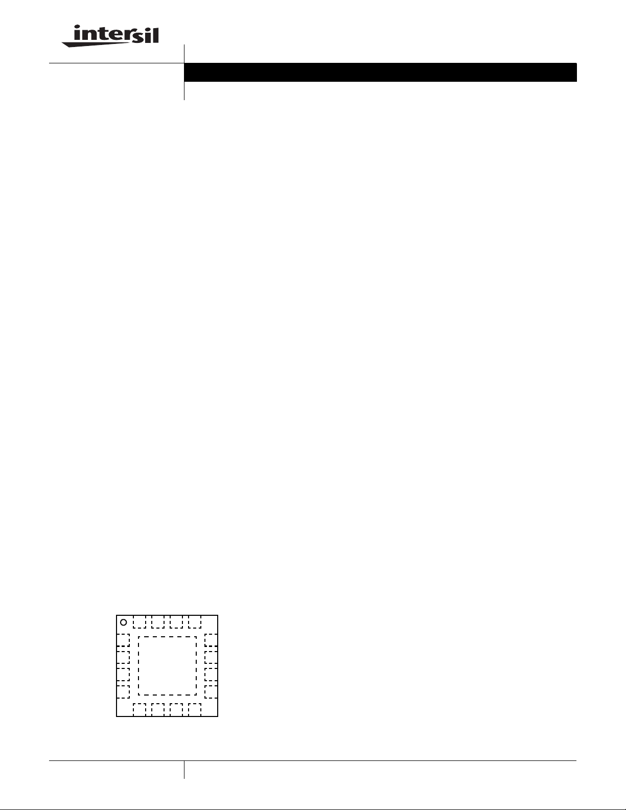
Pinout
VIN
VCC
FCCM
EN
16 LD QFN (4mm x 4mm)
TOP VIEW
PGOOD
LX
1516 14 13
1
2
3
4
GND
6578
FB
COMP
TGATE
FSET
BOOT
12
11
10
VO
1
9
PVCC
BGATE
PGND
BSOC
• Telecom/datacom applications
• Industrial applications
• Distributed DC/DC power architecture
• Point-of-load modules
CAUTION: These devices are sensitive to electrostatic discharge; follow proper IC Handling Procedures.
1-888-INTERSIL or 1-888-468-3774
| Intersil (and design) is a registered trademark of Intersil Americas Inc.
All other trademarks mentioned are the property of their respective owners.
Copyright Intersil Americas Inc. 2006. All Rights Reserved
ISL8106
Ordering Information
PART NUMBER PART MARKING TEMP (°C) PACKAGE PKG. DWG. #
ISL8106CRZ* 8106CRZ 0 to +70 16 Ld 4x4 QFN L16.4x4
ISL8106IRZ* 8106IRZ -40 to +85 16 Ld 4x4 QFN L16.4x4
ISL8106EVAL1Z Evaluation Board
*Add “-T” suffix for tape and reel.
NOTE: Intersil Pb-free plus anneal products employ special Pb-free material sets; molding compounds/die attach materials and 100% matte tin plate
termination finish, which are RoHS compliant and compatible with both SnPb and Pb-free soldering operations. Intersil Pb-free products are MSL
classified at Pb-free peak reflow temperatures that meet or exceed the Pb-free requirements of IPC/JEDEC J STD-020.
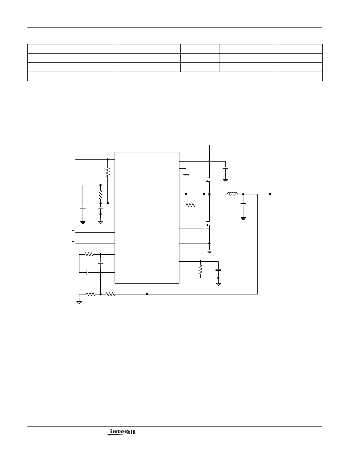
Typical Application
V
IN
+7V TO +25V
PGOOD
PGOOD
R
PGOOD
PVCC
R
VCC
VCC
C
PVCC
C
VCC
GND
ISL8106
FCCM
EN
R
COMP
VIN
BOOT
TGATE
LX
BSOC
BGATE
PGND
CBOOT
R
BSOC
C
IN
Q
TS
L
OUT
C
OUT
Q
BS
V
OUT
COMP
FSET
C
COMP1
C
COMP2
R
BOT
FB
R
VO
R
TOP
FSET
C
FSET
2
FN9283.1
November 10, 2006
Block Diagram
VIN
GND
VCC
3
EN
PACKAGE BOTT OM
V
REF
−
OVP
+
−
UVP
+
LDO
+
+
gmV
−
gmV
−
PWM FREQUENCY
CONTROL
−
+
IN
V
W
−
+
R
PWM
V
R
O
+
C
R
V
COMP
−
+
Q
S
−
VO
FSET
ISL8106
BOOT
+
EA
FB
−
EA
POR
DRIVER
DIGITAL SOFT-START
TGATE
COMP
BSOC
November 10, 2006
PGOOD
FN9283.1
−
I
OC
OCP
+
30Ω
90Ω
60Ω
150°OT
PWM CONTROL
SHOOT THROUGH
PROTECTION
DRIVER
LX
PVCC
BGATE
PGND
FCCM
ISL8106
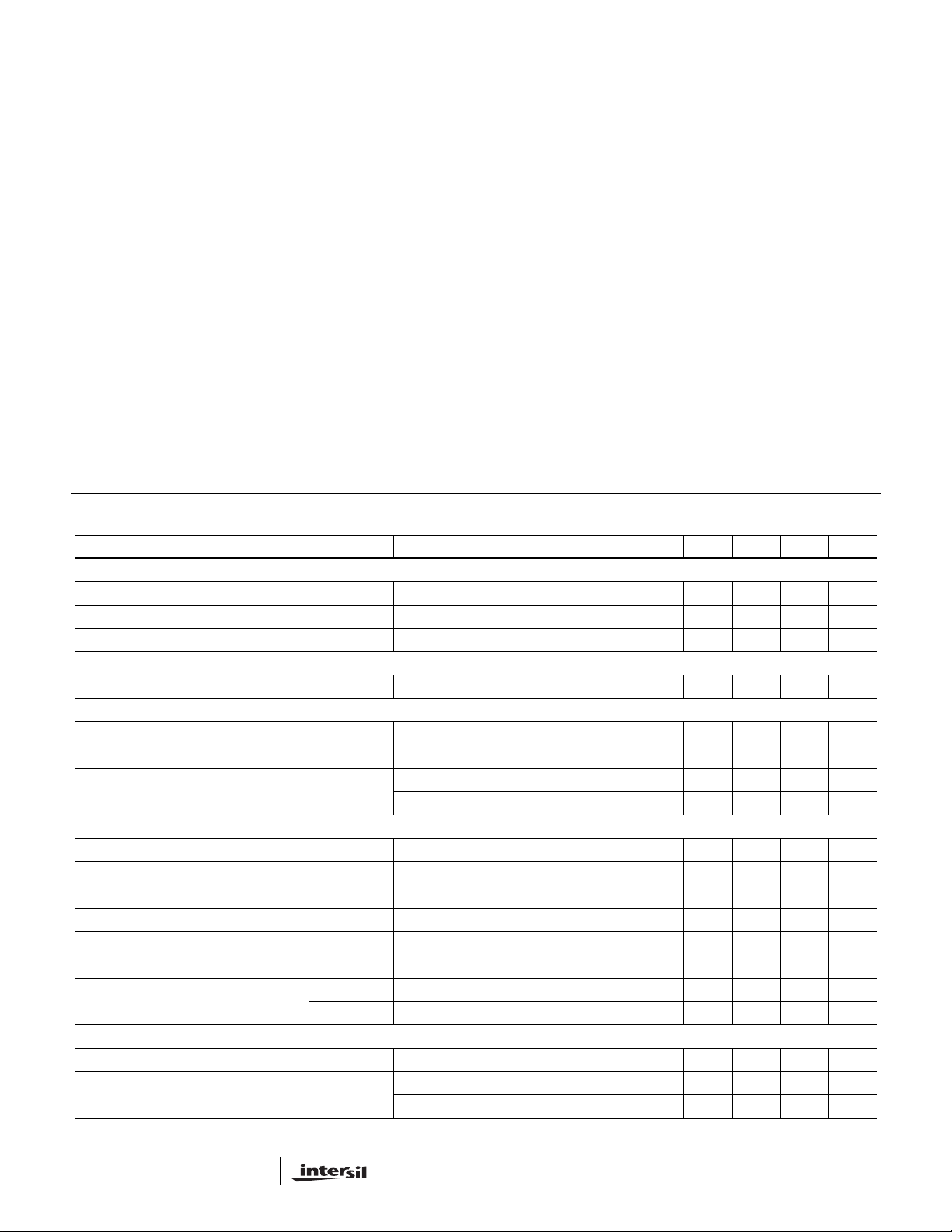
Absolute Voltage Ratings
BSOC, VIN to GND. . . . . . . . . . . . . . . . . . . . . . . . . . . -0.3V to +28V
VCC, PGOOD to GND . . . . . . . . . . . . . . . . . . . . . . . .-0.3V to +7.0V
PVCC to PGND. . . . . . . . . . . . . . . . . . . . . . . . . . . . . .-0.3V to +7.0V
GND to PGND. . . . . . . . . . . . . . . . . . . . . . . . . . . . . . .-0.3V to +0.3 V
EN, FCCM. . . . . . . . . . . . . . . . . . . . . . . . -0.3V to GND, VCC +3.3V
LX to GND. . . . . . . . . . . . . . . . . . . . . . . . . . . . . . (DC) -0.3V to +28V
. . . . . . . . . . . . . . . . . . . . . . . . . . (<100ns Pulse Width, 10μJ) -5.0V
BOOT to GND, or PGND . . . . . . . . . . . . . . . . . . . . . . -0.3V to +33V
BOOT to LX . . . . . . . . . . . . . . . . . . . . . . . . . . . . . . . . . -0.3V to +7V
TGATE . . . . . . . . . . . . . . . . . . . . . . .(DC) -0.3V to LX, BOOT +0.3V
. . . . . . . . . . . . . . . . . . . . . . . . . . (<200ns Pulse Width, 20μJ) -4.0V
BGATE . . . . . . . . . . . . . . . . . . . .(DC) -0.3V to PGND, PVCC +0.3V
. . . . . . . . . . . . . . . . . . . . . . . . . . . (<100ns Pulse Width, 4μJ) -2.0V
ESD Classification . . . . . . . . . . . . . . . . . . . . . .Level 1 (HBM = 2kV)
CAUTION: Stress above those listed in “Absolut e Ma ximum Rat ings ” may ca use pe rmanen t damage t o the de vi ce . Th is is a stress onl y ra tin g an d operat ion of th e device
at these or any other conditions above those indicated in the operational section of this specification is not implied.
NOTES:
is measured in free air with the component mounted on a high effective thermal conductivity test board with “direct attach” features. See T ech
1. θ
JA
Brief TB379.
2. For θ
3. Parameters are Guaranteed by Design.
, the “case temp” location is the center of the exposed metal pad on the package underside.
JC
Thermal Information
Thermal Resistance (Typical, Notes 1, 2) θJA (°C/W) θJC (°C/W)
QFN Package . . . . . . . . . . . . . . . . . . . 48 11.5
Junction Temperature Range . . . . . . . . . . . . . . . . . -55°C to +150°C
Operating Temperature Range
ISL8106CRZ. . . . . . . . . . . . . . . . . . . . . . . . . . . . . . 0°C to +70°C
ISL8106IRZ . . . . . . . . . . . . . . . . . . . . . . . . . . . . -40°C to +85°C
Storage Temperature . . . . . . . . . . . . . . . . . . . . . . . -65°C to +150°C
Lead Temperature . . . . . . . . . . . . . . . . . . . . (soldering, 10s)+300°C
Recommended Operating Conditions
Ambient Temperature Range (ISL8106C) . . . . . . . . . .0°C to +70°C
Ambient Temperature Range (ISL8106I) . . . . . . . . . -40°C to +85°C
Supply Voltage (VIN to GND). . . . . . . . . . . . . . . . . . . . . . 7V to 25V
Electrical Specifications Recommended Operating Conditions, unless otherwise noted specifications in bold are valid for process,
temperature, and line operating conditions.
PARAMETER SYMBOL TEST CONDITIONS MIN TYP MAX UNIT
VIN
VIN Voltage Range V
VIN Input Bias Current I
VIN Shutdown Current I
VCC LDO
VCC Output Voltage Range V
VCC POR THRESHOLD
Rising VCC POR Threshold Voltage
Falling VCC POR Threshold Voltage
CONTROL INPUTS
EN High Threshold Voltage V
EN Low Threshold Voltage V
FCCM High Threshold Voltage V
FCCM Low Threshold Voltage V
EN Leakage Current
FCCM Leakage Current
REFERENCE
Reference Voltage V
Voltage Regulation Accuracy
SHDN
V
CCTHR
V
CCTHF
ENTHR
ENTHF
FCCMTHR
FCCMTHF
I
I
FCCML
I
FCCMH
V
VIN
CC
I
ENL
ENH
REF
REG
IN
EN and FCCM = 5V, FB = 0.65V, VIN = 7V to 25V 2.2 3.0 mA
EN = GND, VIN = 25V 0.1 1.0 μA
VIN = 7V to 25V, I
ISL8106CRZ 4.35 4.45 4.55 V
ISL8106IRZ 4.33 4.45 4.55 V
ISL8106CRZ 4.10 4.20 4.30 V
ISL8106IRZ 4.08 4.20 4.30 V
EN = 0V <0.1 1.0 μA
EN = 5.0V 20 μA
FCCM = 0V <0.1 1.0 μA
FCCM = 5.0V 2.0 μA
ISL8106CRZ -0.6 +0.6 %
ISL8106IRZ -1.0 +1.0 %
= 0mA to 80mA 4.75 5.00 5.25 V
LDO
7.0 25.0 V
2.0 V
0.5 V
2.0 V
1.0 V
0.6 V
4
FN9283.1
November 10, 2006

ISL8106
Electrical Specifications Recommended Operating Conditions, unless otherwise noted specifications in bold are valid for process,
temperature, and line operating conditions.
PARAMETER SYMBOL TEST CONDITIONS MIN TYP MAX UNIT
PWM
F
OSC
Frequency Range
Frequency-Set Accuracy
VO Range V
VO Input Leakage Current
ERROR AMPLIFIER
FB Input Bias Current I
COMP Source Current I
COMP Sink Current I
COMP High Clamp Voltage V
COMP Low Clamp Voltage V
GATE DRIVER
TGATE Pull-Up Resistance R
TGATE Source Current I
TGATE Sink Resistance R
TGATE Sink Current I
BGATE Pull-Up Resistance R
BGATE Source Current I
BGATE Sink Resistance R
BGATE Sink Current I
Delay From TGATE Falling to BGATE
Rising
Delay From BGATE Falling to TGATE
Rising
BOOTSTRAP DIODE
Forward Voltage V
Reverse Leakage I
POWER GOOD
PGOOD Pull Down Impedance
PGOOD Leakage Current I
PGOOD Maximum Sink Current 5.0 mA
F
AUDIO
VO
I
VO
FB
COMPSRC
COMPSNK
COMPHC
COMPLC
TGATEPU
TGATESRCVTGATE
TGATEPD
TGATESNKVTGATE
BGATEPU
BGATESRCVBGATE
BGATEPD
BGATESNKVBGATE
t
TGATEFBG
ATER
t
BGATEFTG
ATER
F
R
PGR
PGR
PGR
PGR
PGR
PGR
PGOOD
FCCM = 5V 200 600 kHz
FCCM = GND; ISL8106CRZ 21 28 kHz
FCCM = GND; ISL8106IRZ 20 28 kHz
F
= 300kHz; ISL8106CRZ -10 +10 %
OSC
= 300kHz; ISL8106IRZ -12 +12 %
F
OSC
0.60 3.30 V
VO = 0.60V
VO = 3.30V
FB = 0.60V ± 20 nA
FB = 0.40V, COMP = 3.20V 2.5 mA
FB = 0.80V, COMP = 0.30V 0.3 mA
FB = 0.40V, Sink 50μA 3.10 3.40 3.65 V
FB = 0.80V, Source 50μA 0.09 0.15 0.21 V
200mA Source Current (Note 3) 1.0 1.5 Ω
1.3
7.0
to LX = 2.5V 2.0 A
250mA Sink Current (Note 3) 1.0 1.5 Ω
to LX = 2.5V 2.0 A
250mA Source Current (Note 3) 1.0 1.5 Ω
to PGND = 2.5V 2.0 A
250mA Sink Current (Note 3) 0.5 0.9 Ω
to PGND = 2.5V 4.0 A
TGATE falling to BGATE rising 21 ns
BGATE falling to TGATE rising 14 ns
PVCC = 5V, IF = 2mA 0.58 V
VR = 25V 0.2 μA
SS
PGOOD = 5mA Sink; ISL8106CRZ 75 95 115 Ω
UV
SS
PGOOD = 5mA Sink; ISL8106IRZ 67 95 118 Ω
UV
PGOOD = 5mA Sink; ISL8106CRZ 50 63 78 Ω
OV
PGOOD = 5mA Sink; ISL8106IRZ 45 63 81 Ω
PGOOD = 5mA Sink; ISL8016CRZ 25 32 40 Ω
OC
PGOOD = 5mA Sink; ISL8106IRZ 22 32 43 Ω
PGOOD = 5V <0.1 1.0 μA
μA
μA
5
FN9283.1
November 10, 2006

ISL8106
Electrical Specifications Recommended Operating Conditions, unless otherwise noted specifications in bold are valid for process,
temperature, and line operating conditions.
PARAMETER SYMBOL TEST CONDITIONS MIN TYP MAX UNIT
T
PGOOD Soft-Start Delay
PROTECTION
BSOC OCP Threshold Current
BSOC Short-Circuit Threshold Current I
UVP Threshold Voltage V
OVP Rising Threshold Voltage V
OVP Falling Threshold Voltage V
OTP Rising Threshold Temperature T
OTP Temperature Hysteresis T
SS
I
OC
SC
UV
OVR
OVF
OTR
OTHYS
Functional Pin Descriptions
GND (Bottom terminal pad)
Signal common of the IC. Unless otherwise stated, signals
are referenced to the GND pin, not the PGND pin. Co nnect
the GND pad of the ISL8106 to the signal ground layer of the
pcb using at least five vias, for a robust thermal and
electrical conduction path.
The best tie-point between the signal ground and the po wer
ground is at the negative side of the output capacitors that is
not in the return path of the inductor ripple current flowing
through the output capacitors.
VIN (Pin 1)
The VIN pin measures the converter input voltage with
respect to the GND pin. VIN is a required input to the R
PWM modulator. The VIN pin is also the input source for the
integrated +5V LDO regulator.
VCC (Pin 2)
The VCC pin is the output of the integrated +5V LDO regulator,
which provides the bias voltage for the IC. The VCC pin
delivers regulated +5V whenever the EN pin is pulled above
V
1µF MLCC decouple capacitor to the GND pin.
FCCM (Pin 3)
The FCCM pin configures the controller to operate in forcedcontinuous-conduction-mode (FCCM) or diode-emulationmode (DEM). DEM is disabled when the FCCM pin is pulled
above the rising threshold voltage V
enabled when the FCCM pin is pulled below the falling
threshold voltage V
EN (Pin 4)
The EN pin is the on/off switch of the IC. When the EN pin is
pulled above the rising threshold voltage V
ramp up and begin regulation. The soft-start sequence
begins once V
. For best performance, the LDO requires at least a
ENTHR
FCCMTHR
FCCMTHF.
ramps above the power-on reset (POR)
CC
ENTHR, VCC
EN High to PGOOD High; ISL8106CRZ 2.20 2.75 3.30 ms
EN High to PGOOD High; ISL8106IRZ 2.20 2.75 3.50 ms
ISL8106CRZ -33 -26 -19 μA
ISL8106IRZ -33 -26 -17 μA
-50 μA
81 84 87 %
113 116 119 %
103 %
(Note 3) 150 °C
(Note 3) 25 °C
rising threshold voltage V
below the falling threshold voltage V
immediately stops and V
threshold voltage V
CC
CCTHF
. When the EN pin is pulled
CCTHR
ENTHF
, PWM
decays below the POR falling
, at which time the IC turns off.
COMP (Pin 5)
The COMP pin is the output of the control-loop error
amplifier. Loop compensation components connect from the
COMP pin to the FB pin.
FB (Pin 6)
The FB pin is the inverting input of the control loop error
amplifier. The converter will regulate to 600mV at the FB pin
with respect to the GND pin. Scale the desired output
voltage to 600mV with a voltage divider network made from
3
resistors R
TOP
and R
BOTTOM
. Loop compensation
components connect from the FB pin to the COMP pin.
FSET (Pin 7)
The FSET pin programs the PWM switching frequency of the
converter. Connect a resistor R
C
from the FSET pin to the GND pin.
FSET
and a 10nF capacitor
FSET
VO (Pin 8)
, and DEM is
will
The VO pin makes a direct measurement of the converter
output voltage used exclusively by the R
The VO pin should be connected to the top of feedback
resistor R
at the converter output. Refer to Typical
TOP
Application Schematic.
BSOC (Pin 9)
The BSOC pin is the input to the overcurrent protection
(OCP) and short-circuit protection (SCP) circuits. Connect a
resistor R
Select the value of R
source the I
inductor current reaches the desired OCP setpoint. The SCP
threshold current I
current I
between the BSOC pin and the LX pin.
BSOC
OC
threshold current IOC when the peak
BSOC
SC
.
that will force the BSOC pin to
BSOC
is fixed at twice the OCP threshold
3
PWM modulator.
6
FN9283.1
November 10, 2006

ISL8106
PGND (Pin 10)
The PGND pin should be connected to the source of the
bottom-side MOSFET , preferably with an isolated path that is
in parallel with the trace connecting the BGATE pin to the
gate of the MOSFET . The PGND pin is an isolated path used
exclusively to conduct the turn-off transient current that flows
out the PGND pin, through the gate-source capacitance of
the bottom-side MOSFET, into the BGATE pin, and back to
the PGND pin through the pull-down resistance of the
BGA TE driver. The adaptive shoot-through protection circuit,
measures the bottom-side MOSFET gate voltage with
respect to the PGND pin, not the GND pin.
BGATE (Pin 11)
The BGATE pin is the output of the bottom-side MOSFET
gate driver. Connect to the gate of the bottom-side MOSFET.
The signal going through this trace is both high dv/dt and
high di/dt, with high peak charging and discharging current.
Route this trace in parallel with the trace from the PGND pin.
These two traces should be short, wide, and away from
other traces. There should be no other weak signal traces in
parallel with these traces on any layer.
PVCC (Pin 12)
The PVCC pin is the input voltage for the bottom-side
MOSFET gate driver BGATE. Connect a +5V power source
to the PVCC pin with respect to the GND pin, a 1µF MLCC
bypass capacitor needs to be connected from the PVCC pin
to the PGND pin, not the GND pin. The VCC output may be
used for the PVCC input voltage source. Connect the VCC
pin to the PVCC pin through a low-pass filter consisting of a
resistor and the PVCC bypass capacitor. Refer to Typical
Application Schematic.
BOOT (Pin 13)
The BOOT pin stores the input voltage for the top-side
MOSFET gate driver. Connect an MLCC capacitor across
the BOOT and LX pins. The boot capacitor is charged
through an internal boot diode connected from the PVCC pin
to the BOOT pin, each time the LX pin drops below PVCC
minus the voltage dropped across the internal boot diode.
TGATE (Pin 14)
The TGATE pin is the output of the top- si de MOSFET gate
driver. Connect to the gate of the top-side MOSFET.
The signal going through this trace is both high dv/dt and
high di/dt, with high peak charging and discharging current.
Route this trace in parallel with the trace from the LX pin.
These two traces should be short, wide, and away from
other traces. There should be no other weak signal traces in
parallel with these traces on any layer.
the bottom-side MOSFET drain voltage for the diode
emulation function.
Connect the LX pin to the node consisting of the top-side
MOSFET source, the bottom-side MOSFET drain, and the
output inductor. Refer to Typical Application Schematic. This
trace should be short, and positioned away from other weak
signal traces. The parasitic capacitance and parasitic
inductance of the LX node should be kept very low to
minimize ringing. If ringing is excessive, it could easily affect
current sample information. It would be best to limit the size
of the LX node copper in strict accordance with the current
and thermal management of the application.
PGOOD (Pin 16)
The PGOOD pin is an open-drain output that is high
impedance when the converter is in regulation, or when the
EN pin is pulled below the falling threshold voltage V
ENTHF
The PGOOD pin has three distinct pull-down impedances
that correspond to an OVP fault, OCP/SCP, or UVP and softstart. Connect the PGOOD pin to +5V through a pull-up
resistor.
Functional Description
POR and Soft-Start
The power-on reset (POR) circuit monitors VCC for the
V
(rising) and V
CCR
purpose of soft-start is to limit the inrush current through the
output capacitors when the converter first turns on. The
PWM soft-start sequence initializes once V
the V
threshold, beginning from below the V
CCR
threshold.
The ISL8106 uses a digital soft-start circuit to ramp the
output voltage of the converter to the programmed regulation
setpoint in approximately 1.5ms. Th e co nve r t er re gu l at e s to
600mV at the FB pin with respect to the GND pin. During
soft-start a digitally derived voltage reference forces the
converter to regulate from 0V to 600mV at the FB pin. When
the EN pin is pulled above the rising EN threshold volt age
V
the PGOOD Soft-Start Delay TSS begins and the
ENTHR
output voltage begins to rise. The output voltage enters
regulation in approximately 1.5ms and the PGOOD pin goes
to high impedance once T
When the EN pin is pulled below the V
LDO stops regulating and PWM immediately stops,
regardless of the falling V
sequence can be reinitialized and fault latches reset, once
V
falls below the V
CC
(falling) voltage thresholds. The
CCF
rises above
CC
has elapsed.
SS
threshold, the
ENF
voltage. The soft-start
CC
threshold.
CCF
CCF
.
LX (Pin 15)
The LX pin is the return current path for the TGATE
MOSFET driver. The LX pin also measures the polarity of
7
FN9283.1
November 10, 2006

EN
V
OUT
1.5ms
PGOOD
2.75ms
FIGURE 1. SOFT-START SEQUENCE
PGOOD
The PGOOD pin connects to three open drain MOSFETS
each of which has a different r
undefined impedance if V
threshold V
V
. The ISL8106 features a unique fault-identification
CCF
, or if VCC is below the falling POR threshold
CCR
has not reached the rising POR
CC
capability that can drastically reduce trouble-shooting time
and effort. The pull-down resistance of the PGOOD pin
corresponds to the fault status of the controller. During softstart or if an undervoltage fault occurs, the PGOOD pulldown
resistance is 95Ω, or 30Ω for an o vercurre nt faul t, or 60 Ω for
an overvoltage fault.
TABLE 1. PGOOD PULL-DOWN RESISTANCE
CONDITION PGOOD RESISTANCE
IC Off Open
Soft-Start 95Ω
Undervoltage Fault 95Ω
Overvoltage Fault 60Ω
Overcurrent Fault 30Ω
. The PGOOD pin is an
DS(ON)
ISL8106
can simultaneously affect the PWM switching frequency and
PWM duty cycle in response to input voltage and output load
transients. The term “Ripple” in the name “Robust-RippleRegulator” refers to the converter output inductor ripple
current, not the converter output ripple voltage. The output
voltage is regulated to 600mV at the FB pin with respect to
the GND pin. The FB pin is the inverting input of the error
amplifier. The frequency response of the feedback control
loop is tuned with a type-two compensation network
connected across the FB pin and COMP pin.
3
The R
modulator synthesizes an AC signal VR, which is an
ideal representation of the output inductor ripple current. The
duty-cycle of V
is derived from the voltage measured at the
R
VIN pin and VO pin with respect to the GND pin.
Transconductance amplifiers convert the VIN and VO
voltages into currents that charge and discharge the ripple
capacitor C
V
RPOS
The negative slope of V
V
RNEG
A voltage V
output voltage V
into which voltage V
. The positive slope of VR can be written as:
R
gm()VINVO–()•=
can be written as:
R
gm V
•=
O
is referenced with respect to the error amplifier
W
, creating a window-voltage envelope
COMP
is compared. The V
R
R, VCOMP,
and VW
(EQ. 1)
(EQ. 2)
signals feed into a hysteretic window comparator in which
V
threshold voltage. PWM pulses are generated as V
traverses the V
discharging rates of capacitor C
switching frequency for a given amplitude of V
to V
is the lower threshold voltage and VW is the higher
COMP
and V
W
. The R3 regulator simultaneously affects switching
COMP
thresholds. The charging and
COMP
determine the PWM
R
R
with respect
W
frequency and duty cycle because it modulates both edges
of the PWM pulses.
LDO
Voltage applied to the VIN pin with respect to the GND pin is
regulated to +5VDC by an internal low-dropout voltage
regulator (LDO). The output of the LDO is called V
CC
, which
is the bias voltage used by the IC internal circuitry. The LDO
output is routed to the VCC pin and requires a ceramic
capacitor connected to the GND pin to stabilize the LDO and
to decouple load transients.
When the EN pin rises above the V
threshold, VCC will
ENR
turn on and rise to its regulation voltage. The LDO regulates
V
by pulling up towards the voltage at the VIN pin; the
CC
LDO has no pull-down capability.
Pulse Width Modulator
The ISL8106 is a hybrid of fixed frequency PWM control, and
variable frequency hysteretic control. Intersil’s R
8
3
technology
Ripple Capacitor Voltage C
FIGURE 2. MODULATOR W A VEFORMS DURING LOAD
TRANSIENT
R
Window Voltage V
Error Amplifier Voltage V
PWM
November 10, 2006
W
COMP
FN9283.1

ISL8106
MOSFET Gate-Drivers
The ISL8106 has internal gate-drivers for the top-side and
bottom-side N-Channel MOSFETs. The bottom-side gatedriver is optimized for low duty-cycle applications where the
bottom-side MOSFET conduction losses are dominant,
requiring a low r
resistance is small in order to clamp the gate of the MOSFET
below the V
GS(th)
the gate at turnoff can be considerable because the
switching charge of a low r
Both drivers incorporate bottom-side MOSFETS from
conducting simultaneously and shorting the input supply.
During turn-off of the bottom-side MOSFET, the BGATE to
PGND voltage is monitored until it reaches a 1V threshold, at
which time the TGATE driver is allowed to switch. During
turn-off of the top-side MOSFET, the TGATE to LX voltage is
monitored until it reaches a 1V threshold, at which time the
BGATE driver is allowed to switch.
The input power for the BGATE driver circuit is sourced
directly from the PVCC pin. The input power for the TGATE
driver circuit is sourced from a “boot” capacitor connected
from the BOOT pin to the LX pin. The boot capacitor is
charged from a 5V bias supply through a internal Schottky
diode each time the bottom-side MOSFET turns on.
MOSFET. The BGATE pulldown
DS(on)
at turnoff. The current transient through
MOSFET can be large.
DS(on)
rectifier, switching the bottom-side MOSFET regardless of
the polarity of the output inductor current. In DEM, the
bottom-side MOSFET is disabled during negative current
flow from the output inductor. DEM is permitted when the
FCCM pin is pulled low, and disabled when pulled high.
When DEM is permitted, the converter will automatically
select FCCM or DEM according to load conditions. If positive
LX pin voltage is measured for eight consecutive PWM
pulses, then the converter will enter diode-emulation mode
on the next PWM cycle. If a negative LX pin voltage is
measured, the converter will exit DEM on the following PWM
pulse. An audio filter is incorporated into the PWM
generation circuitry that prevents the switching frequency
from entering the audible spectrum at low load conditions.
Overcurrent and Short-Circuit Protection
When an OCP or SCP fault is detected, the ISL8106
overcurrent and short-circuit protection circuit will pull the
PGOOD pin low and latch off the converter. The fault will
remain latched until the EN pin is pulled below V
voltage at the VIN pin is reduced to the extent that V
fallen below the POR V
appropriate value of resistor R
threshold. Selecting the
CCF
that is connected from
BSOC
the BSOC pin to the drain terminal of the bottom-side
MOSFET to programs the OCP threshold.
ENF
or if the
has
CC
TGATE
BGATE
t
BGFTGR
FIGURE 3. GATE DRIVE TIMING DIAGRAM
t
TGFBGR
50%
50%
Diode Emulation
Positive inductor current can flow from the source of the topside MOSFET or from the drain of the bottom-side MOSFET.
Negative inductor current flows into the drain of the bottomside MOSFET. When the bottom-side MOSFET conducts
positive inductor current, the LX voltage will be negative with
respect to the GND pin. Conversely, when the bottom-side
MOSFET conducts negative inductor current, the LX voltage
will be positive with respect to the GND pin. Negative
inductor current occurs when the output load current is less
than ½ the inductor ripple current.
The OCP circuit measures positive-flowing, peak-current
through the output inductor, not the DC current flowing from
the converter to the load. The bottom-side MOSFET drain
current is assumed to be equal to the positive output
inductor current when the top-side MOSFET is turn off.
Current briefly conducts through the bottom-side MOSFET
body diode until the BGATE driver goes high. The peak
inductor current develops a voltage across the r
DS(ON)
of
the bottom-side MOSFET just as if it were a discrete currentsense resistor. An OCP fault will occur when the BSOC pin
has measured more than the OCP threshold current I
OC,
on
consecutive PWM pulses, for a period exceeding 20µs. It
does not matter how many PWM pulses are measured
during the 20µs period. If a measurement falls below I
OC
before 20µs has elapsed, then the timer is reset to zero. An
SCP fault will occur when the BSOC pin has measured more
than the short-circuit threshold current I
in less than
SC,
10µs, on consecutive PWM pulses. The relationship
between I
I
BSOCRBSOC
The value of R
R
BSOC
and I
D
• I
BSOC
I
+ OC
FL
----------------------------------------------------------------------------
=
can be written as:
BSOC
•=
DrDS ON()
can then be written as:
I
PP
-------- -
• r
I
SP
OC
2
•
DS ON()
(EQ. 3)
(EQ. 4)
The ISL8106 can be configured to operate in forcedcontinuous-conduction-mode (FCCM) or in diode-emulationmode (DEM), which can improve light-load efficiency. In
FCCM, the controller always operates as a synchronous
9
FN9283.1
November 10, 2006

ISL8106
Where:
-R
(Ω) is the resistor used to program the over-
BSOC
current setpoint
-I
is the current sense current that is sourced from
BSOC
the BSOC pin
-I
OC
is the I
threshold current value sourced from
BSOC
the BSOC pin that will activate the OCP circuit
is the maximum continuous DC load current
-I
FL
is the inductor peak-to-peak ripple current
-I
PP
-OCSP is the desired overcurrent setpoint expressed as
a multiplier relative to I
FL
Overvoltage
When an OVP fault is detected, the ISL8106 overvoltage
protection circuit will pull the PGOOD pin low and latch off
the converter. The fault will remain latched until the EN pin is
pulled below V
to the extent that V
or if the voltage at the VIN pin is reduced
ENF
has fallen below the POR V
CC
CCF
threshold.
When the voltage at the FB pin (relative to the GND pin) has
exceeded the rising overvoltage threshold V
OVR
, the
converter will latch off; however, the BGA TE driver output will
stay high, forcing the bottom-side MOSFET to pull down the
output voltage of the converter. The bottom-side MOSFET
will continue to pull down the output voltage until the voltage
at the FB pin relative to the GND pin, has decayed below the
falling overvoltage threshold V
at which time the BGA TE
OVF,
driver output is driven low, forcing the bottom-side MOSFET
off. The BGATE driver output will continue to switch on at
V
and switch off at V
OVR
V
or if the voltage at the VIN is reduced to the extent that
ENF
V
has fallen below the POR V
CC
until the EN pin is pulled below
OVF
threshold.
CCF
UnderVoltage
When an UVP fault is detected, the ISL8106 undervoltage
protection circuit will pull the PGOOD pin low and latch off
the converter. The UVP fault occurs when the voltage at the
FB pin relative to the GND pin, has fallen below the undervoltage threshold V
EN pin is pulled below V
reduced to the extent that V
V
threshold.
CCF
The fault will remain latched until the
UV .
or if the voltage at the VIN is
ENF
has fallen below the POR
CC
Over-Temperature
When an OTP fault is detected, the ISL8106 overtemperature protection circuit suspends PWM, but will not
affect the PGOOD pin, or latch off the converter. The overtemperature protection circuit measures the temperature of
the silicon and activates when the rising threshold
temperature T
suspended until the silicon temperature falls below the
temperature hysteresis T
operation is resumed. All other protection circuits will
function normally during OTP however, since PWM is
inhibited, it is likely that the converter will immediately
experience an undervoltage fault, latch off, and pull PGOOD
has been exceeded. The PWM remains
OTR
at which time normal
OTHYS
low. If the EN pin is pulled below V
VIN is reduced to the extent that V
POR V
threshold, normal operation will resume
CCF
however, the temperature hysteresis T
or if the voltage at the
ENF
has fallen below the
CC
is reset.
OTHYS
Application Guidelines
Layout Considerations
As in any high frequency switching converter, layout is very
important. Switching current from one power device to
another can generate voltage transients across the
impedances of the interconnecting bond wires and circuit
traces. These interconnecting impedances should be
minimized by using wide, short printed circuit traces. The
critical components should be located as close together as
possible using ground plane construction or single point
grounding.
A multi-layer printed circuit board is recommended. Figure 4
shows the critical components of the converter. Note that
capacitors C
physical capacitors. Dedicate one solid layer, usually a
middle layer of the PC board, for a ground plane and make
all critical component ground connections with vias to this
layer. Dedicate another solid layer as a power plane and
break this plane into smaller islands of common voltage
KEY
FIGURE 4. PRINTED CIRCUIT BOARD POWER PLANES
and C
IN
VCC
PVCC
ISL8106
TGATE
BOOT
LX
BGATE
PGND
GND
TRACE SIZED FOR 4A PEAK CURRENT
SHORT TRACE, MINIMUM IMPEDANCE
ISLAND ON POWER PLANE LAYER
ISLAND ON CIRCUIT AND/OR POWER PLANE LAYER
VIA CONNECTION TO GROUND PLANE
AND ISLANDS
could each represent numerous
OUT
C
BP_PVCC
C
BP_VCC
C
IN
R
VCC
VIN
C
Q
Q
IN
1
L
OUT
C
OUT
2
V
OUT
LOAD
10
FN9283.1
November 10, 2006

ISL8106
levels. Keep the metal runs from the LX terminals to the
output inductor short. The power plane should support the
input power and output power nodes. Use copper filled
polygons on the top and bottom circuit layers for the LX
nodes. Use the remaining printed circuit layers for small
signal wiring.
Locate the ISL8106 within 2 to 3 inches of the MOSFETs, Q1
and Q2 (1 inch or less for 500kHz or higher operation). The
circuit traces for the MOSFET s’ gate and source connections
from the ISL8106 must be sized to handle up to 4A peak
current. Provide local V
GND pins. Locate the capacitor, C
decoupling between VCC and
CC
as close as practical
BOOT
to the BOOT pin and the phase node.
Programming the Output Voltage
When the converter is in regulation there will be 600mV from
the FB pin to the GND pin. Connect a two-resistor voltage
divider across the VO pin and the GND pin with the output
node connected to the FB pin. Scale the voltage-divider
network such that the FB pin is 600mV with respect to the
GND pin when the converter is regul a ti ng at the desired
output voltage.
Programming the output voltage can be written as:
R
V
REFVOUT
BOTTOM
•=
---------------------------------------------------
R
+
TOPRBOTTOM
(EQ. 5)
Where:
-V
-V
is the desired output voltage of the converter.
OUT
is the voltage that the converter regulates to at the
REF
FB pin.
-R
is the voltage-programming resistor that connects
TOP
from the FB pin to the VO pin. It is usually c hose n to set
the gain of the control-loop error amplifier. It follows that
R
BOTTOM
selected value of R
-R
BOTTOM
will be calculated based upon the already
TOP .
is the voltage-programming resistor that
connects from the FB pin to the GND pin.
Calculating the value of R
V
R•
REF
R
BOTTOM
-------------------------------------
=
V
TOP
–
OUTVREF
BOTTOM
can now be written as:
(EQ. 6)
Programming the PWM Switching Frequency
The PWM switching frequency F
resistor R
that is connected from the FSET pin to the
FSET
GND pin. Programming the approximate PWM switching
frequency can be written as:
•
FSET
OSC
1
110
×[]•
1
1
×10[]••
12–
FSET
12–
-------------------------------------------------------------- -
=
F
OSC
60 R
Estimating the value of R
R
FSET
--------------------------------------------------------
=
60 F
is programmed by the
OSC
can now be written as:
(EQ. 7)
(EQ. 8)
Where:
-F
-R
- 60 x [1 x 10
is the PWM switching frequency.
OSC
FSET
is the F
-12
programming resistor.
OSC
] is a constant.
Selection of the LC Output Filter
The duty cycle of a buck converter is ideally a function of the
input voltage and the output voltage. This relationship can be
written as:
()
DV
Where:
- D is the PWM duty cycle.
-VIN is the input voltage to be converted.
-V
The output inductor peak-to-peak ripple current can be
written as:
I
PP
Where:
-I
-F
-L
A typical step-down DC/DC converter will have an I
20% to 40% of the nominal DC output load current. The
value of I
MOSFET switching loss, inductor core loss, and the
resistance the inductor winding, DCR. The DC copper loss of
the inductor can be estimated by:
P
COPPERILOAD
The inductor copper loss can be significant in the total
system power loss. Attention has to be given to the DCR
selection. Another factor to consider when choosing the
inductor is its saturation characteristics at elevated
temperature. A saturated inductor could cause destruction of
circuit components, as well as nuisance OCP faults.
A DC/DC buck regulator must have output capacitance C
into which ripple current I
corresponding ripple voltage V
sum of the voltage drop across the capacitor ESR and of the
voltage change stemming from charge moved in and out of
the capacitor. These two voltages can be written as:
ΔV
and
ΔV
If the output of the converter has to support a load with high
pulsating current, several capacitors will need to be
V
OUT
--------------- -
=
IN
V
IN
is the regulated output voltage of the converter.
OUT
V
1DVIN()–[]•
OUT
-----------------------------------------------------
=
F
•
OSCLO
is the peak-to-peak output inductor ripple current.
PP
is the PWM switching frequency.
OSC
is the nominal value of the output inductor.
O
is selected based upon several criteria such as
PP
[]2DCR•=
can flow. Current IPP develops a
ESRIPP
-----------------------------------
=
C
8COF•
•
I
PP
E• SR=
PP
OSC
across C
PP
which is the
O,
(EQ. 9)
(EQ. 10)
of
PP
(EQ. 11)
(EQ. 12)
(EQ. 13)
O
11
FN9283.1
November 10, 2006

ISL8106
paralleled to adjust the ESR to achieve the required VPP.
The inductance of the capacitor can cause a brief voltage dip
when the load transient has an extremely high slew rate.
Low inductance capacitors constructed with reverse
package geometry are available.
A capacitor dissipates heat as a function of RMS current. Be
sure that I
is shared by a sufficient quantity of paralleled
PP
capacitors so that they operate below the maximum rated
RMS current. Take into account that the specified value of a
capacitor can drop as much as 50% as the D C voltage
across it increases.
Selection of the Input Capacitor
The important parameters for the bulk input capacitance are
the voltage rating and the RMS current rating. For reliable
operation, select bulk capacitors with voltage and current
ratings above the maximum input voltage and capable of
supplying the RMS current required by the switching circuit.
Their voltage rating should be at least 1.25 times greater
than the maximum input voltage, while a voltage rating of 1.5
times is a preferred rating. Figure 5 is a graph of the input
RMS ripple current, normalized relative to output loa d current,
as a function of duty cycle that is adjusted for converter
efficiency. The ripple current calculation is written as:
I
IN_RMS
2
I
-----------------------------------------------------------------------------------------------------
=
MAX
DD2–()⋅()xI
⎛⎞
+
⎝⎠
I
MAX
Where:
-I
is the maximum continuous I
MAX
- x is a multiplier (0 to 1) corresponding to the inductor
peak-to-peak ripple amplitude expressed as a
percentage of I
(0% to 100%)
MAX
- D is the duty cycle that is adjusted to take into account
the efficiency of the converter which is written as:
V
OUT
--------------------------
D
=
VINEFF⋅
0.6
0.55
0.5
0.45
0.4
0.35
0.3
0.25
0.2
0.15
0.1
0.05
0
NORMALIZED INPUT RMS RIPPLE CURRENT
0 0.1 0.2 0.3 0.4 0.5 0.6 0.7 0.8 0.9 1
FIGURE 5. NORMALIZED RMS INPUT CURRENT FOR x = 0.8
x = 1
x = 0.75
x = 0.50
x = 0.25
x = 0
DUTY CYCLE
2
D
MAX
------
12
of the converter
LOAD
⋅⋅
(EQ. 14)
In addition to the bulk capacitance, some low ESL ceramic
capacitance is recommended to decouple between the drain
terminal of the top-side MOSFET and the source terminal of
the bottom-side MOSFET, in order to reduce the voltage
ringing created by the switching current across parasitic
circuit elements.
MOSFET Selection and Considerations
Typically, MOSFETS cannot tolerate even brief excursions
beyond their maximum drain to source voltage rating. The
MOSFETS used in the power conversion stage of the
converter should have a maximum V
the upper voltage tolerance of the input power source, and
the voltage spike that occurs when the MOSFET switches
off. Placing a low ESR ceramic capacitor as close as
practical across the drain of the top-side MOSFET and the
source of the bottom-side MOSFET will reduce the
amplitude of the turn-off voltage spike.
The MOSFET input capacitance C
source resistance r
related; reduction of r
of C
. These two parameters affect the efficiency of the
ISS
, are to an extent, inversely
DS(ON)
typically results in an increase
DS(ON)
converter in different ways. The r
loss when the MOSFET is completely turned on and
conducting current. The C
affects the power loss when
ISS
the MOSFET is actively switching. Switching time increases
as C
increases. When the MOSFET switches it will briefly
ISS
conduct current while the drain to source voltage is still
present. The power dissipation during this time is substantial
so it must be kept as short as practical. Often the top-side
MOSFET and the bottom-side MOSFET are different
devices due to the trade-offs that have to be made between
C
ISS
and r
DS(ON)
.
The bottom-side MOSFET power loss is dominated by
r
PWM switching cycle; the r
because it conducts current for the majority of the
DS(ON)
DS(ON)
switching loss is small for the bottom-side MOSFET even
though C
is large due to the low r
ISS
because the drain to source voltage is clamped by the body
diode. The top-side MOSFET power loss is dominated by
C
because it conducts current for the minority of the
ISS
PWM switching cycle; the C
should be small. The
ISS
switching loss of the top-side MOSFET is large compared to
the bottom-side MOSFET because the drain to source
voltage is not clamped. For the bottom-side MOSFET, its
power loss can be assumed to be the conduction loss only
and can be written as:
P
CONBSDVIN
()⋅ I
[]2r•
LOAD
DS ON()BS
For the top-side MOSFET, its conduction loss can be written
as:
P
CONTSDVIN
()⋅ I
[]2r•
LOAD
DS ON()TS
rating that exceeds
DS
and on-state drain to
ISS,
affects the power
DS(ON)
should be small. The
of the device,
DS(ON)
1DVIN()–[]•≈
D• VIN()=
(EQ. 15)
(EQ. 16)
12
FN9283.1
November 10, 2006

ISL8106
For the top-side MOSFET, its switching loss can be written
as:
P
SWTSVIN
()
V
INIVALTON
-------------------------------------------------------------
F•
••
2
V
OSC
INIPEAKTOFF
-------------------------------------------------------------------- -
+=
F•
••
OSC
2
(EQ. 17)
The peak and valley current of the inductor can be obtained
based on the inductor peak-to-peak current and the load
current. The turn-on and turn-off time can be estimated with
the given gate driver parameters in the Electrical
Specification Table.
Selecting The Bootstrap Capacitor
The selection of the bootstrap capacitor can be written as:
Q
g
------------------------
BOOT
=
ΔV
BOOT
(EQ. 18)
C
Where:
is the total gate charge required to switch the top-
-Q
g
side MOSFET
- ΔV
, is the maximum allowed voltage decay across
BOOT
the boot capacitor each time the MOSFET is switched on
As an example, suppose the top-side MOSFET has a total
gate charge Q
, of 25nC at VGS= 5V, and a ΔV
G
BOOT
of
200mV. The calculated bootstrap capacitance is 0.125µF;
select at least the first standard component value of greater
capacitance than calculated, that being 0.15µF. Use an X7R
or X5R ceramic capacitor.
Compensating the Converter
The LC output filter has a double pole at its resonant frequency
that causes the phase to abruptly roll downward. The R
modulator used in the ISL8106 makes the LC output filter
resemble a first order system in which the closed loop stability
can be achieved with a Type II compensation network.
C
COMP1
C
COMP2
R
TOP
V
REF
FB
−
ERROR
AMPLIFIER
+
R
COMP
COMP
3
Figure 7 highlights the voltage-mode control loop for a
synchronous-rectified buck converter. The output voltage is
regulated to the reference voltage level. The error amplifier
output is compared with the oscillator triangle wave to
provide a pulse-width modulated wave with an amplitude of
V
at the LX node. The PWM wave is smoothed by the
IN
output filter. The output filter capacitor bank’s equivalent
series resistance is represented by the series resistor ESR.
C
COMP1
R
COMP
COMP
EA
C
COMP2
R
R
BOTTOM
TOP
FB
-
+
REF
VO
R3 Modulator
Gate Drivers
ISL8106
GND
FSET
VIN
TGATE
LX
BGATE
R
FSET
Q
Q
VIN
TOP_SIDE
L
OUT
BOTTOM_SIDE
C
DCR
C
OUT
ESR
FSET
FIGURE 6. SYSTEM CONTROL BLOCK DIAGRAM
13
FIGURE 7. COMPENSATION REFERENCE CIRCUIT
November 10, 2006
FN9283.1

ISL8106
The control loop model of the ISL8106 is partitioned into
function blocks consisting of:
- The duty cycle to Vo transfer function G
(s) which is
VD
determined by the value of the output power
components, input voltage, and output voltage.
- The Vcomp to duty cycle transfer function F
(s) which
m
is determined by the PWM frequency, input voltage,
output voltage, resistor R
, and capacitor C
FSET
FSET.
- The product of the GVD(s) and Fm(s) transfer functions
is expressed as the V
G
VOVC
(s).
- The type-two compensation network G
to Vo transfer function
COMP
COMP
(s) that
connects across the COMP and FB pins.
- The product of the G
COMP
(s) and G
VOVC
(s) transfer
functions is expressed as the l oop t ransfer f unctio n T(s) .
T(s)=G
V
REF
+
−
COMP
FIGURE 8. SYSTEM CONTROL BLOCK DIAGRAM
COMP
(s)
(s) x G
V
VOVC
COMP
(s)
G
VOVC
(s)G
The compensator transfer function can be written as:
s
--------- -
ω
1
•
+
i
ω
G
COMP
s()
=
----------------------------------
s1
z1
s
----------
•
+
ω
p1
(EQ. 19)
where the compensator zero fz1 is
-------------------------------------------------
=
ω
z1
R
1
•
COMPCCOMP2
(EQ. 20)
Vcomp to Vo Transfer Function Gvovc(s)
1.10
90
60
30
0
30
Phase
60
90
120
150
6
120
100
80
60
40
20
Gain (db)
0
20
40
10 100 1.10
Gain (Gvovc)
Phase (Gvovc)
3
1.10
Frequency (Hz)
4
FIGURE 9. OPEN LOOP TRANSFER FUNCTION
1.10
5
Voltage Loop Gain T(s)
1.10
90
75
60
45
30
Phase
15
0
15
30
6
120
V
o
100
80
60
40
20
Gain (db)
0
20
40
10 100 1.10
Gain (Tv)
Phase (Tv)
3
1.10
Frequency (Hz)
4
1.10
5
FIGURE 10. CLOSED LOOP TRANSFER FUNCTION
ω
z1
--------- -
f
z1
=
2 π•
(EQ. 21)
the compensator pole fp1 is
------------------------
+
C
COMP2
1
•=
---------------------
R
COMP
1
(EQ. 22)
(EQ. 23)
1
p1
p1
=
------------------------
C
COMP1
ω
p1
----------
2 π•
ω
f
and
------------------------------------------------------------------------------------- -
ω
=
i
R
COMPCCOMP1CCOMP2
1
+[]•
(EQ. 24)
The Your local Intersil representative can provide a PCbased tool that can be used to calculate compensation
network component values and help simulate the loop
frequency response. The compe n s a ti o n ne t w o r k c o n si s t s o f
the internal error amplifier of the ISL8106 and the external
components R
the frequency setting components R
TOP
, R
COMP
, C
COMP1
, and C
FSET
COMP2
, and C
as well as
FSET,
are
identified in the schematic Figure 7.
14
FN9283.1
November 10, 2006

ISL8106
Quad Flat No-Lead Plastic Package (QFN)
Micro Lead Frame Plastic Package (MLFP)
L16.4x4
16 LEAD QUAD FLAT NO-LEAD PLASTIC PACKAGE
(COMPLIANT TO JEDEC MO-220-VGGC ISSUE C)
MILLIMETERS
SYMBOL
A 0.80 0.90 1.00 -
A1 - - 0.05 -
A2 - - 1.00 9
A3 0.20 REF 9
b 0.23 0.28 0.35 5, 8
D 4.00 BSC -
D1 3.75 BSC 9
D2 1.95 2.10 2.25 7, 8
E 4.00 BSC -
E1 3.75 BSC 9
E2 1.95 2.10 2.25 7, 8
e 0.65 BSC -
k0.25 - - -
L 0.50 0.60 0.75 8
L1 - - 0.15 10
N162
Nd 4 3
Ne 4 3
P- -0.609
θ --129
NOTES:
1. Dimensioning and tolerances conform to ASME Y14.5-1994.
2. N is the number of terminals.
3. Nd and Ne refer to the number of terminals on each D and E.
4. All dimensions are in millimeters. Angles are in degrees.
5. Dimension b applies to the metallized terminal and is measured
between 0.15mm and 0.30mm from the terminal tip.
6. The configuration of the pin #1 identifier is optional, but must be
located within the zone indicated. The pin #1 identifier may be
either a mold or mark feature.
7. Dimensions D2 and E2 are for the exposed pads which provide
improved electrical and thermal performance.
8. Nominal dimensions are provided to assist with PCB Land Pattern
Design efforts, see Intersil Technical Brief TB389.
9. Features and dimensions A2, A3, D1, E1, P & θ are present when
Anvil singulation method is used and not present for saw
singulation.
10. Depending on the method of lead termination at the edge of the
package, a maximum 0.15mm pull back (L1) maybe present. L
minus L1 to be equal to or greater than 0.3mm.
NOTESMIN NOMINAL MAX
Rev. 5 5/04
All Intersil U.S. products are manufactured, assembled and tested utilizing ISO9000 quality systems.
Intersil Corporation’s quality certifications can be viewed at www.intersil.com/design/quality
Intersil products are sold by description only. Intersil Corporation reserves the right to make changes in circuit design, software and/or specifications at any time without
notice. Accordingly, the reader is cautioned to verify that data sheets are current before placing orders. Information furnished by Intersil is believed to be accurate and
reliable. However, no responsibility is assumed by Intersil or its subsidiaries for its use; nor for any infringements of patents or other rights of third parties which may result
from its use. No license is granted by implicat ion or oth erwise u nde r any p a tent or p at ent r ights of Intersil or its subsidiaries.
For information regarding Intersil Corporation and its products, see www.intersil.com
15
FN9283.1
November 10, 2006
 Loading...