®
ISL8104
Data Sheet November 10, 2006 FN9257.1
8V to 14V, Single-Phase Synchronous
Buck Pulse-Width Modulation (PWM)
Controller With Integrated Gate Drivers
The ISL8104 is a 8V to 14V synchronous PWM controller
with integrated MOSFET drivers. The controller features the
ability to safely start-up into prebiased output loads and
provides protection against overcurrent fault events.
Overcurrent protection is implemented using top-side
MOSFET r
sensing, eliminating the need for a current
DS(ON)
sensing resistor.
The ISL8104 employs voltage-mode control with dual-edge
modulation to achieve fast transient response. The operating
frequency is adjustable from 50kHz to 1.5MHz with full (0%
to 100%) PWM duty cycle capability. The error amplifier
features a 15MHz (typ) gain-bandwidth product and 6V/µs
slew rate enabling high converter bandwidth.
The output voltage of the converter can be regulated to as
low as 0.597V with a tolerance of ±1.0% over the
commercial temperature range (0°C to +70°C), and ±1.5%
over industrial temperature range (-40°C to +85°C).
Provided in the QFN package, a SS pin and REFIN pin
enable supply sequencing and voltage tracking functionality.
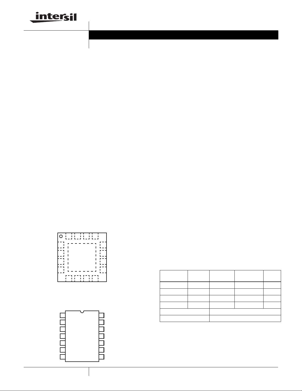
Pinouts
ISL8104 (16 LD QFN)
TOP VIEW
Features
• +8V ±5% to +14V ±10% Bias Voltage Range
- 1.5V to 15.4V Input Voltage Range
• 0.597V Internal Reference Voltage
- ±1.0% Over the Commercial Temperature Ran g e
- ±1.5% Over the Industrial Temperature Range
• Voltage-Mode PWM Control with Dual-Edge Modulation
• 14V High Speed N-Channel MOSFET Gate Drivers
- 2.0A Source/3A Sink at 14V Bottom-Side Gate Drive
- 1.25A Source/2A Sink at 14V Top-Side Gate Drive
• Fast Transient Response
- 15MHz (typ) Gain-Bandwidth Error Amplifier with 6V/µs
slew rate
- Full 0% to 100% Duty Cycle Support
• Programmable Operating Frequency from 50kHz to
1.5MHz
• Lossless Programmable Overcurrent Protecti on
- Top-Side MOSFET’s r
DS(ON)
Sensing
- ~120ns Blanking Time
• Sourcing and Sinking Current Capability
• Support for Start-Up into Prebiased Loads
• Soft-Start Done and an External Reference Pin for
Tracking Applications are Available in the QFN Package
• Pb-Free Plus Anneal Available (RoHS Compliant)
Applications
TSOC
SSDONE
SS
1
COMP
2
FB
3
EN
4
REFIN
ISL8104 (14 LD NARROW SOIC)
1
FSET
2
TSOC
SS
3
COMP
4
FB
5
EN
6
GND
7
FSET
1516 14 13
6578
LX
GND
TOP VIEW
1
VCC
TGATE
14
13
12
11
10
12
11
10
9
9
8
PVCC
BGATE
PGND
BOOT
VCC
PVCC
BGATE
PGND
BOOT
TGATE
LX
• Test and Measurement Instruments
• Distributed DC/DC Power Architecture
• Industrial Applications
• Telecom/Datacom Applica ti on s
Ordering Information
PART #
(Note)
ISL8104CBZ 8104CBZ 0 to +70 14 Ld SOIC M14.15
ISL8104IBZ 8104IBZ -40 to +85 14 Ld SOIC M14.15
ISL8104CRZ 8104CRZ 0 to +70 16 Ld 4x4 QFN L16.4x4
ISL8104IRZ 8104IRZ -40 to +85 16 Ld 4x4 QFN L16.4x4
ISL8104EVAL1Z Evaluation Board
ISL8104EVAL2Z Evaluation Board
*Add “-T” suffix for tape and reel.
NOTE: Intersil Pb-free plus anneal products employ special Pb-free
material sets; molding compounds/die attach materials and 100% matte
tin plate termination finish, which are RoHS compliant and compatible
with both SnPb and Pb-free soldering operations. Intersil Pb-free
products are MSL classified at Pb-free peak reflow temperatures that
meet or exceed the Pb-free requirements of IPC/JEDEC J STD-020.
CAUTION: These devices are sensitive to electrostatic discharge; follow proper IC Handling Procedures.
1-888-INTERSIL or 1-888-468-3774
All other trademarks mentioned are the property of their respective owners.
PART
MARKING
| Intersil (and design) is a registered trademark of Intersil Americas Inc.
Copyright Intersil Americas Inc. 2006. All Rights Reserved
TEMP.
RANGE (°C)
PACKAGE
(Pb-free)
PKG.
DWG. #
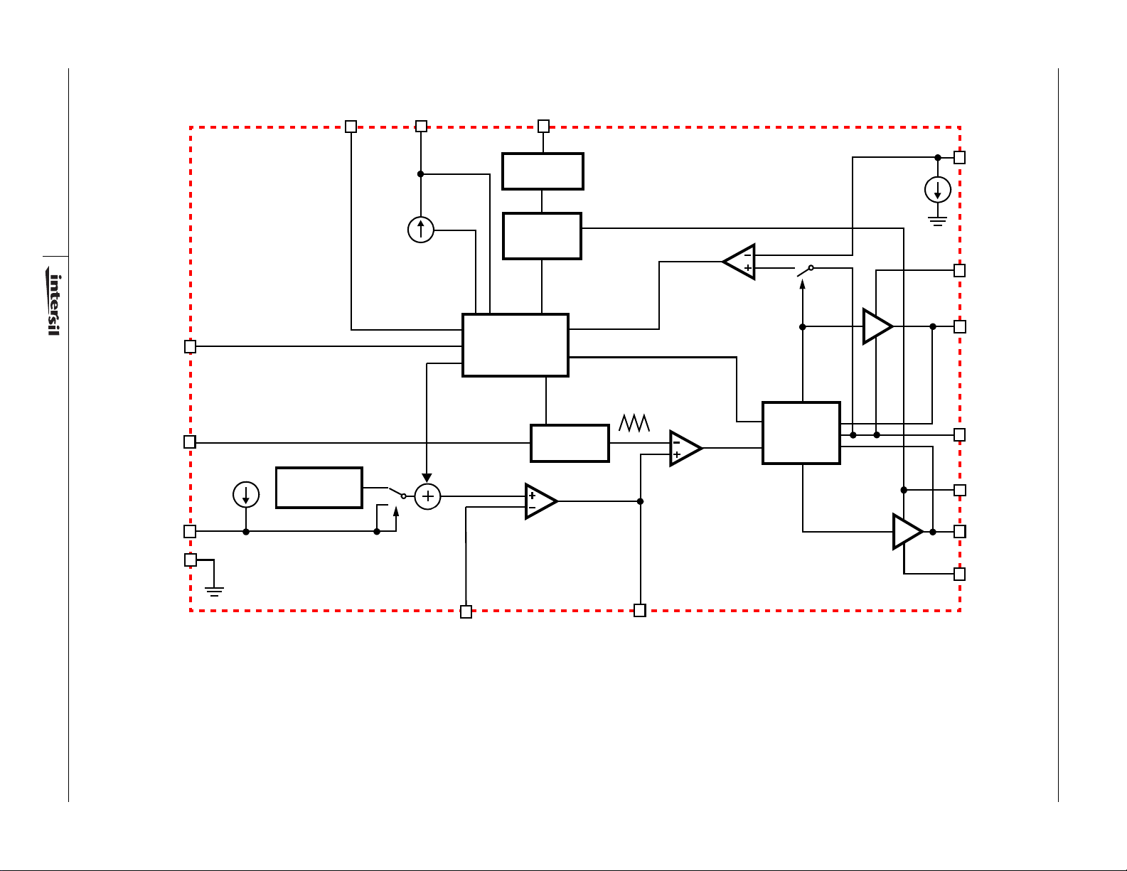
Block Diagram
EN
2
SSDONE
(QFN ONLY)
SS
30μA
VCC
INTERNAL
REGULATOR
POWER-ON
RESET (POR)
SOFT-START
AND
FAULT LOGIC
TSOC
200μA
BOOT
SOURCE OCP
TGATE
ISL8104
GATE
FSET
6μA
REFERENCE
V
= 0.597 V
REF
OSCILLATOR
CONTROL
LOGIC
PWM
LX
PVCC
REFIN
(QFN ONL Y)
GND
FB
November 10, 2006
FN9257.1
EA
BGATE
PGND
COMP
ISL8104
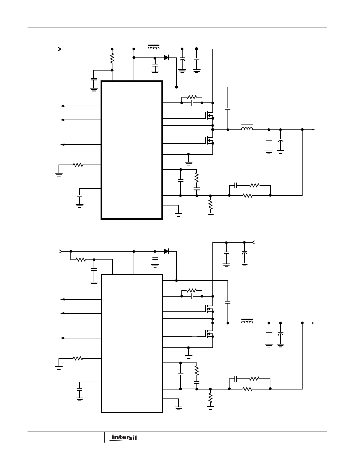
Typical Application with Single Power Supply
+8V to +14V
V
IN
R
FILTER
L
IN
D
C
BOOT
F2
C
C
BIN
HFIN
C
F1
VCC
PVCC
BOOT
R
TSOC
SSDONE
(QFN ONLY)
(QFN ONLY)
R
FSET
C
REFIN
EN
ISL8104
FSET
SS
SS
TSOC
TGATE
LX
BGATE
PGND
COMP
C
FB
GND
C
TSOC
2
Typical Application with Separated Power Supplies
+8V to +14V
V
CC
R
FILTER
C
F1
SSDONE
(QFN ONLY)
REFIN
(QFN ONLY)
VCC
PVCC
D
C
BOOT
F2
BOOT
R
TSOC
TSOC
C
TSOC
TGATE
LX
C
BOOT
Q1
L
OUT
Q2
R
2
C
1
R
C
0
C
HFOUT
R
3
3
R
1
C
BOUT
V
OUT
+1.5V to +15.4V
V
IN
HFIN
C
BOOT
C
BIN
C
Q1
L
OUT
V
OUT
R
FSET
EN
ISL8104
FSET
SS
C
SS
BGATE
PGND
COMP
C
FB
GND
2
3
Q2
R
2
C
1
R
C
0
C
HFOUT
R
3
3
R
1
C
BOUT
November 10, 2006
FN9257.1
ISL8104
Absolute Maximum Ratings Thermal Information
Supply Voltage, V
Enable Voltage, V
Soft-start Done Voltage, V
TSOC Voltage, V
BOOT Voltage, V
LX Voltage, V
PVCC,VVCC
. . . . . . . . . . . . . . . . . . . . .GND - 0.3V to +16V
EN
TSOC
BOOT
. . . . . . . . . . . . . . . . V
LX
. . . . . . . . . . . . . .GND - 0.3V to +16V
SSDONE
. . . . . . . . . .GND - 0.3V to +16V
. . . . . . . . . . . . . . . . . . . .GND - 0.3V to +16V
. . . . . . . . . . . . . . . . . . .GND - 0.3V to +36V
BOOT
- 16V to V
BOOT
+ 0.3V
All Other Pins. . . . . . . . . . . . . . . . . . . . . . . . . . . GND - 0.3V to 5.0V
Thermal Resistance (Typical) θ
SOIC Package (Note 1) . . . . . . . . . . . . 95 N/A
QFN Package (Notes 2, 3). . . . . . . . . . 47 8.5
Maximum Junction Temperature . . . . . . . . . . . . . . . . . . . . . +150°C
Maximum Storage Temperature Range. . . . . . . . . .-65°C to +150°C
Maximum Lead Temperature (Soldering 10s) . . . . . . . . . . . +300°C
(SOIC - Lead tips only)
(°C/W) θJC (°C/W)
JA
Operating Conditions
Supply Voltage, V
Supply Voltage, V
Boot to Phase Voltage, V
. . . . . . . . . . . . . . . . .+8V ±5% to +14V ±10%
VCC
. . . . . . . . . . . . . . . .+8V ±5% to +14V ±10%
PVCC
BOOT
- VLX . . . . . . . . . . . . . . . . . <V
PVCC
ESD Ratings
ESD Classification. . . . . . . . . . . . . . . . . . . . . . . . . . . . . . . . . Class 2
Ambient Temperature Range, ISL8104C. . . . . . . . . . . 0°C to +70°C
Ambient Temperature Range, ISL8104I. . . . . . . . . . .-40°C to +85°C
CAUTION: Stresses above those listed in “Absolute Maximum Ratings” may cause permanent damage to the device. This is a stress only rating and operation of the
device at these or any other conditions above those indicated in the operational sections of this specification is not implied.
NOTES:
is measured with the component mounted on a high effective thermal conductivity test board in free air. See Tech Brief TB379 for details.
1. θ
JA
is measured in free air with the component mounted on a high effective thermal conductivity test board with “direct attach” features. See
2. θ
JA
Tech Brief TB379.
3. For θ
, the “case temp” location is the center of the exposed metal pad on the package underside.
JC
4. Parameters are Guaranteed by Design.
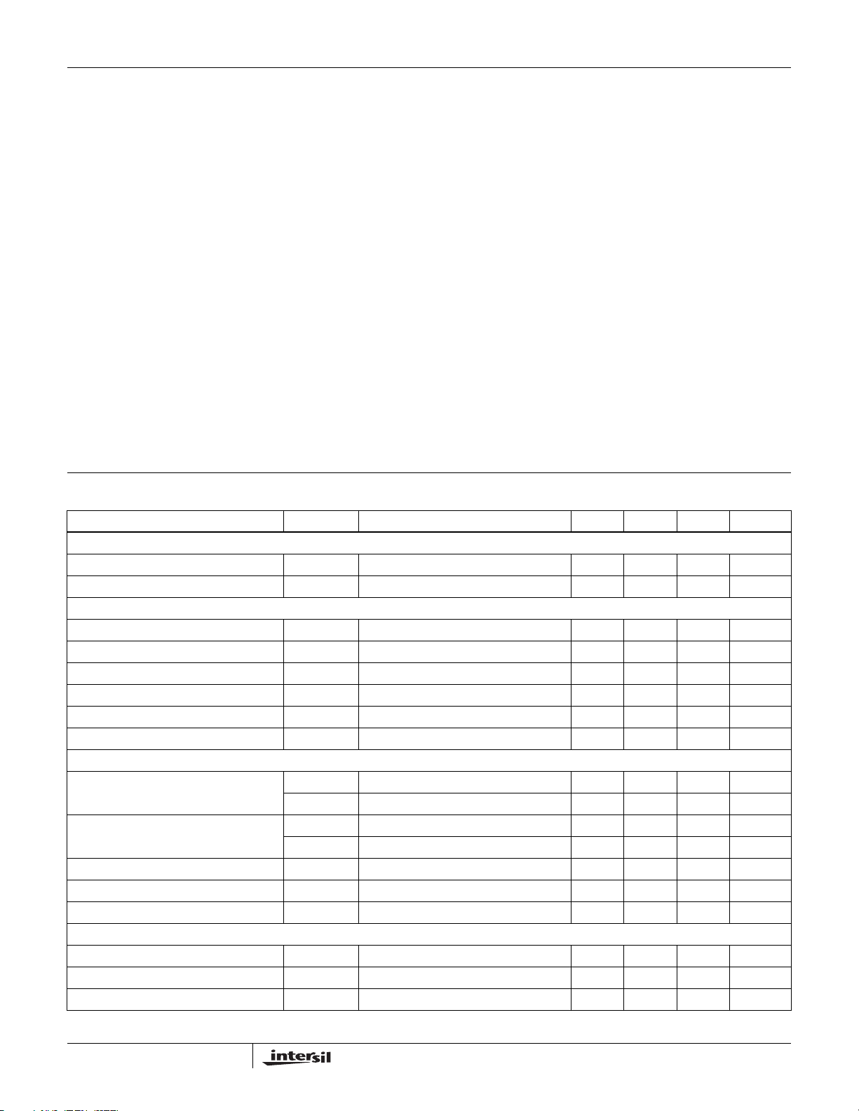
Electrical Specifications Recommended Operating Conditions, unless otherwise noted specifications in bold are valid for process,
temperature, and line operating conditions.
PARAMETER SYMBOL TEST CONDITIONS MIN TYP MAX UNITS
V
SUPPLY CURRENT
CC
Shutdown Supply V
Shutdown Supply V
CC
PVCC
POWER-ON RESET
V
CC/VPVCC
V
CC/VPVCC
Rising Threshold 6.55 7.10 7.55 V
Hysteresis 170 250 500 mV
TSOC Rising Threshold 0.70 0.73 0.75 V
TSOC Hysteresis 180 200 220 mV
Enable - Rising Threshold 1.4 1.5 1.60 V
Enable - Hysteresis 175 250 325 mV
REFERENCE
Reference Voltage T
System Accuracy T
REFIN Current Source (QFN Only) -4 -6 -8 μA
REFIN Threshold (QFN Only) 2.10 - 3.50 V
REFIN Offset (QFN Only) -3 - 3 mV
OSCILLATOR
Trim Test Frequency R
Total Variation (Note 4) 8kΩ < R
Ramp Amplitude ΔV
I
VCC
I
PVCC
OSC
SS/EN = 0V 3.5 6.1 8.5 mA
SS/EN = 0V 0.30 0.5 0.75 mA
= 0°C to +70°C 0.591 0.597 0.603 V
J
T
= -40°C to +85°C 0.588 0.597 0.606 V
J
= 0°C to +70°C -1.0 - 1.0 %
J
= -40°C to +85°C -1.5 - 1.5 %
T
J
= OPEN V
FSET
to GND < 200kΩ - ±15 - %
FSET
R
= OPEN 1.7 1.9 2.15 V
FSET
= 12 175 200 220 kHz
VCC
P-P
4
FN9257.1
November 10, 2006
ISL8104
Electrical Specifications Recommended Operating Conditions, unless otherwise noted specifications in bold are valid for process,
temperature, and line operating conditions. (Continued)
PARAMETER SYMBOL TEST CONDITIONS MIN TYP MAX UNITS
Ramp bottom (Note 4) -1- V
ERROR AMPLIFIER
DC Gain (Note 4) R
Gain-Bandwidth Product (Note 4) GBWP R
Slew Rate (Note 4) SR R
COMP Source Current (Note 4) I
COMP Sink Current (Note 4) I
GATE DRIVERS
Top-side Drive Source Current (Note 4) I
Top-side Drive Source Impedance R
Top-side Drive Sink Current (Note 4) I
Top-side Drive Sink Impedance R
Bottom-side Drive Source Current (Note 4) I
Bottom-side Drive Source Impedance R
Bottom-side Drive Sink Current (Note 4) I
Bottom-side Drive Sink Impedance R
PROTECTION
TSOC Current I
TSOC Measurement Offset (Note 4) OCP
SOFT-START
Soft-start Current I
SSDONE Low Output Voltage
(QFN ONLY)
COMPSRC
COMPSNK
T_SOURCEVBOOT
T_SOURCE
T_SINK
T_SINK
B_SOURCEVPVCC
B_SOURCE
B_SINK
B_SINK
TSOC
OFFSET
SS
= 10kΩ, CL= 100pF - 88 - dB
L
= 10kΩ, CL= 100pF - 15 - MHz
L
= 10kΩ, CL= 100pF - 6 - V/μs
L
-2-mA
-2-mA
- VLX = 14V, 3nF Load - 1.25 - A
90mA Source Current - 2.0 - Ω
V
- VLX = 14V, 3nF Load - 2 - A
BOOT
90mA Source Current - 1.3 - Ω
= 14V, 3nF Load - 2 - A
90mA Source Current - 1.3 - Ω
V
= 14V, 3nF Load - 3 - A
PVCC
90mA Source Current - 0.94 - Ω
TJ = 0°C to +70°C 180 200 220 μA
= -40°C to +85°C 176 200 224 μA
T
J
TSOC = 1.5V to 15.4V - ±10 - mV
22 30 38 μA
I
= 2mA - - 0.30 V
SSDONE
Functional Pin Description (QFN/SOIC)
SS (Pin 1/3)
Connect a capacitor from this pin to ground. This capacitor,
along with an internal 30μA current source, sets the soft-start
interval of the converter.
COMP (Pin 2/4) and FB (Pin 3/5)
COMP and FB are the available external pins of the error
amplifier. The FB pin is the inverting input of the error amplifier and the COMP pin is the error amplifier output. These
pins are used to compensate the voltage-control feedback
loop of the converter.
EN (Pin 4/6)
This pin is a TTL compatible input. Pull this pin below 0.8V to
disable the converter. In shutdown the soft-start pin is
discharged and the TGATE and BGATE pins are held low.
5
REFIN (QFN ONLY Pin 5)
Upon enable if REFIN is less than 2.2V, the external
reference pin is used as the control reference instead of the
internal 0.597V reference. An internal 6
μA pull up to 5V is
provided for disabling this functionality.
GND (Pin 6/7)
Signal ground for the IC. All voltage levels are measured
with respect to this pin.
LX (Pin 7/8)
This pin connects to the source of the top-side MOSFET and
the drain of the bottom-side MOSFET. This pin represents
the return path for the top-side gate driver. During normal
switching, this pin is used for top-side current sensing.
TGATE (Pin 8/9)
Connect TGATE to the top-side MOSFET gate. This pin
provides the gate drive for the top-side MOSFET.
FN9257.1
November 10, 2006
 Loading...