

Page 1
User Guide 009
ISL8011xEVAL1Z Evaluation Board User Guide
Description
The ISL8011xEVAL1Z provides a simple platform to evaluate
performance of the ISL8011x family of split supply LDOs.
Jumpers are provided to easily set popular output voltages.
The ISL80111, ISL80112 and ISL80113 are single-output
LDOs specified for 1A, 2A, 3A of output current and are
optimized for less than 2.5V and less output voltage
conversions. The ISL8011x supports V
provided a standard legacy 2.9V or 5.5V is applied on the
pin. The output voltage is adjustable from 0.8V to 3.3V.
V
BIAS
voltages down to 1V,
IN
Specifications
This board has been configured and optimized for the following
operating conditions:
range of 1V to 3.6V
•V
IN
adjustable from 0.8V to 3.3V
•V
OUT
• Convenient power connection
• Popular output voltages can easily set by jumpers
Key Features
• Ultra low dropout: 75mV at 3A, (typ)
• Excellent V
• ±1.6% guaranteed V
• Very fast load transient response
PSRR: 70dB at 1kHz (typ)
IN
accuracy for -40ºC < TJ < +125ºC
OUT
References
ISL80111, ISL80112, ISL80113 Datasheet
Ordering Information
PART NUMBER DESCRIPTION
ISL80111EVAL1Z 1A, Split Supply LDO Evaluation Board
ISL80112EVAL1Z 2A, Split Supply LDO Evaluation Board
ISL80113EVAL1Z 3A, Split Supply LDO Evaluation Board
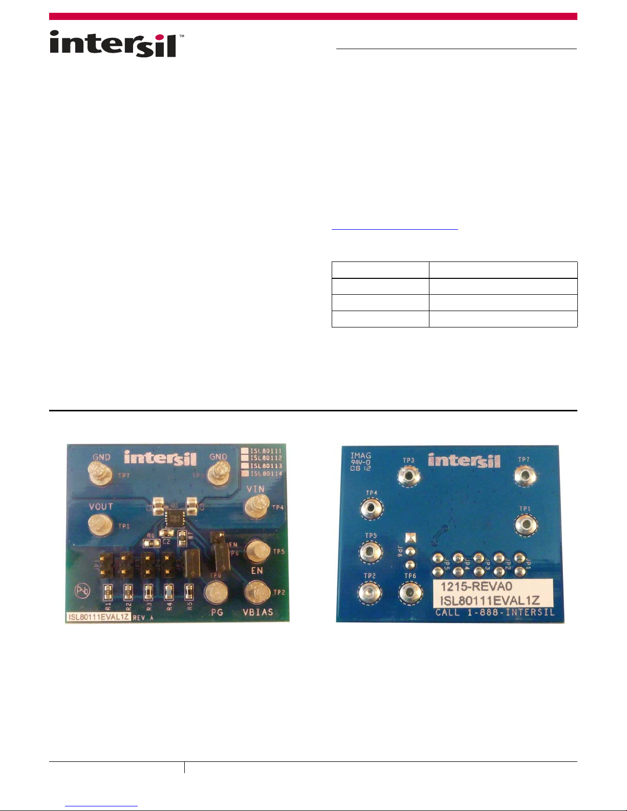
FIGURE 1. ISL80111EVAL1Z TOP SIDE
October 30, 2014
UG009.0
1
FIGURE 2. ISL80111EVAL1Z BOTTOM SIDE
CAUTION: These devices are sensitive to electrostatic discharge; follow proper IC Handling Procedures.
1-888-INTERSIL or 1-888-468-3774
Intersil (and design) is a trademark owned by Intersil Corporation or one of its subsidiaries.
All other trademarks mentioned are the property of their respective owners.
| Copyright Intersil Americas LLC 2014. All Rights Reserved
Page 2
User Guide 009
What’s Inside
The evaluation kit contains the following:
• The ISL80113EVAL1Z with the appropriate parts installed
• ISL80111, ISL80112, ISL80113
Datasheet
Test Steps
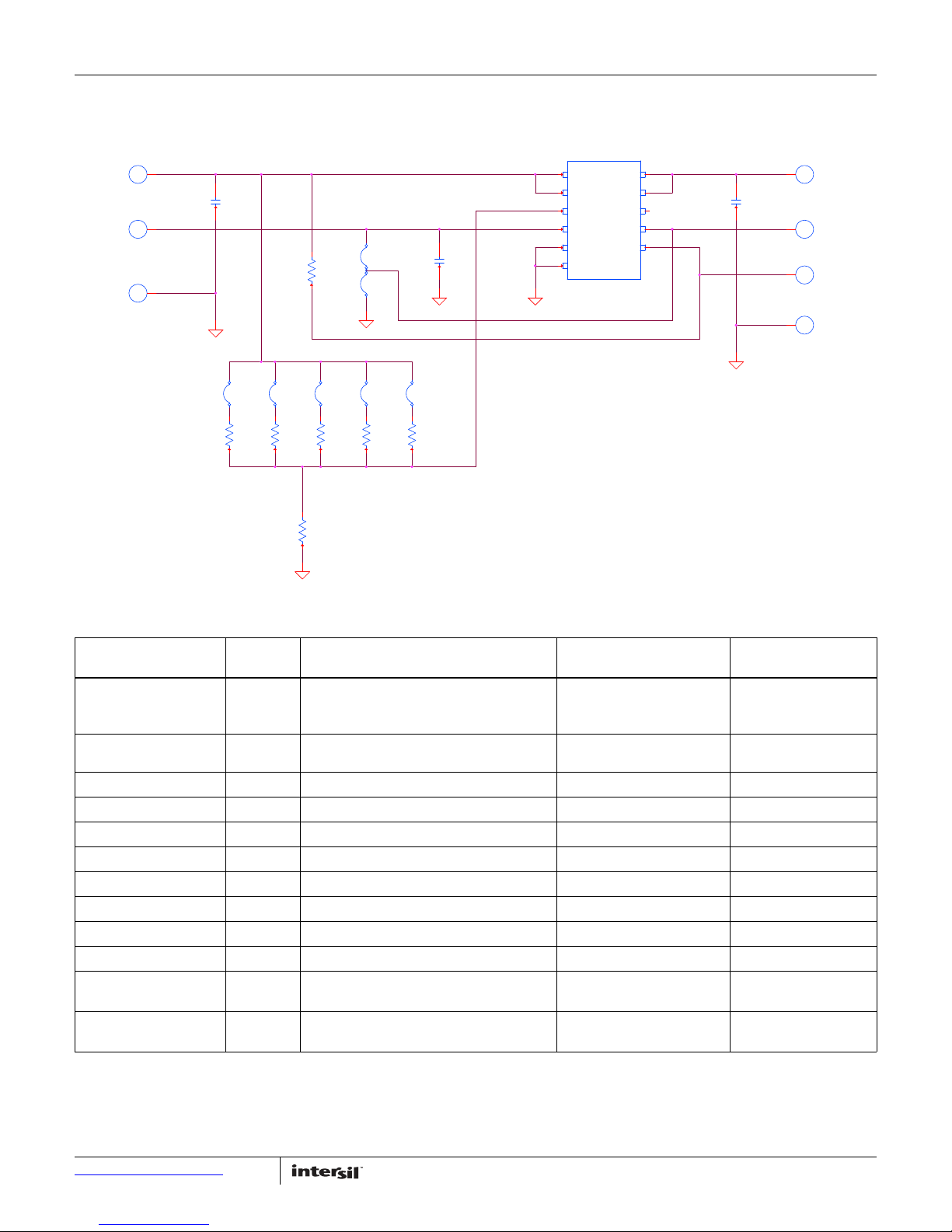
1. Select the desired output voltage by shorting one of the
jumpers from JP2 through JP5.
2. Connect both the BIAS and VIN supplies and the load. Enable
the IC using jumper JP6 (bottom position) or via a signal on
the center post, observe the output.
3. The shipped configuration is enabled and V
4. Scope shots taken from ISL8011xEVAL1Z boards.
OUT
= 3.3V.
Functional Description
The ISL8011xEVAL1Z provides a simple platform to evaluate
performance of the ISL8011x family of split supply LDOs.
Jumpers are provided to easily set popular output voltages.
The ISL80111, ISL80112 and ISL80113 are single-output LDOs
specified for 1A, 2A, 3A of output current and are optimized for
less than 2.5V and less output voltage conversions. The
ISL8011X supports VIN voltages down to 1V, provided a standard
legacy 2.9V or 5.5V is applied on the V
voltage is adjustable from 0.8V to 3.3V.
An enable input, having a threshold <1V, allows the part to be
placed into a low quiescent current shutdown mode. A submicron
CMOS process is utilized for this product family to deliver
best-in-class analog performance and overall value for
applications in need of input voltage conversions to typically
below 2.5V. It also has the superior load transient regulation
unique to a NMOS power stage.
These LDOs consume significantly lower quiescent current as a
function of load compared to bipolar LDOs. This lower
consumption translates into higher efficiency and the ability to
consider packages with smaller footprints. The quiescent current
has been modestly compromised in design to enable leading
class fast load transient response and load regulation.
pin. The output
BIAS
PCB Layout Guidelines
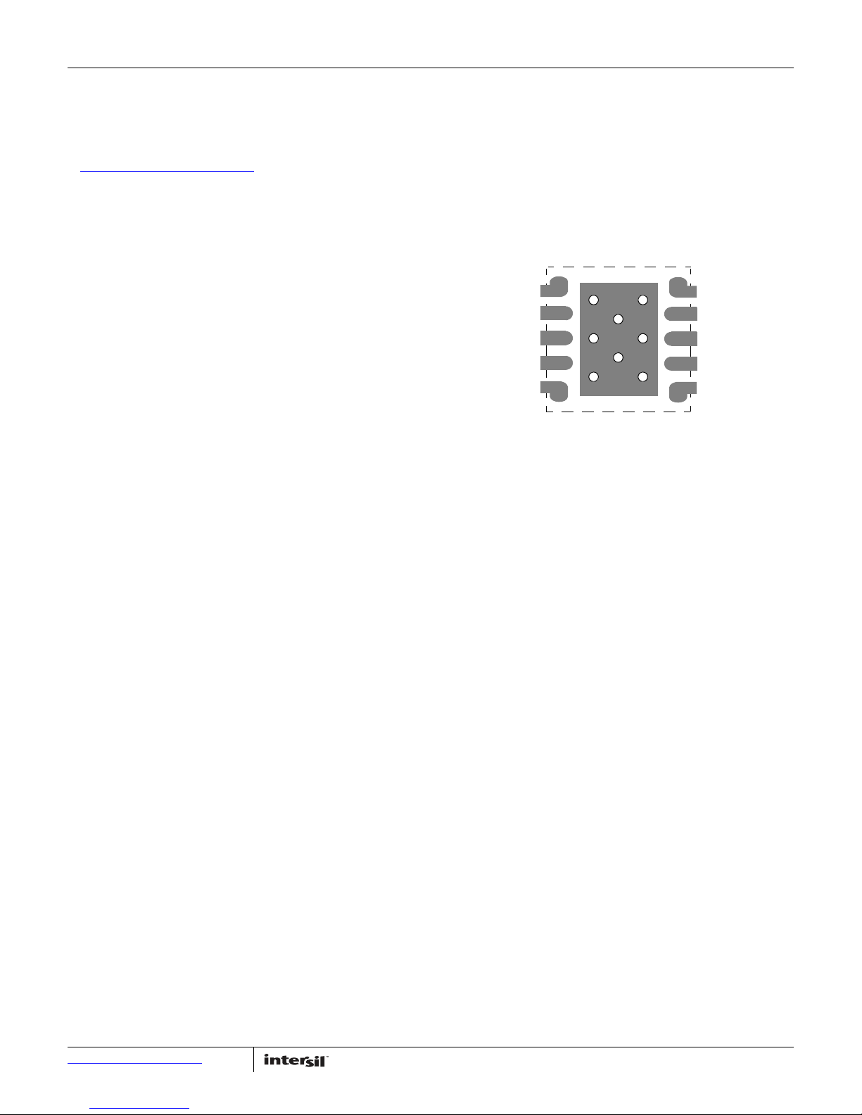
The following is an example of how to use vias to remove heat
from the IC.
Filling the thermal pad area with vias is recommended. A typical
via array is to fill the thermal pad footprint with vias spaced such
that they are center on center 3x the radius apart from each
other. Keep the vias small but not so small that their inside
diameter prevents solder from wicking through the holes during
reflow.
FIGURE 3. PCB VIA PATTERN
Connect all vias to the round plane. For efficient heat transfer, it
is important that the vias have low thermal resistance. Do not
use “thermal relief” patterns to connect the vias. It is important
to have a complete connection of the plated through-hole to each
plane.
Submit Document Feedback
2
UG009.0
October 30, 2014
Page 3
Schematic
EVALUATION BOARD FOR:
GND
ISL80113
GND
ISL80111
ISL80112
1.0V
1.5V
1.8V
2.5V
3.3V
ISL80114
EN
PG
VADJ
VBIAS
VINVOUT
C3
10UF
JP2
JP6
TP3
TP7
5.62K
R5
TP2
TP6
1K
R6
JP5
TP1
TP5
R7
100K
TP4
2.61K
R3
1UF
C2
10UF
C1
JP3
1K
R1
4.02K
R4
EP
VOUT
VOUTNCVIN
VIN
GND
EN
PG
ADJ
VBIAS
ISL80113IRAJZ
U1
1
2
3
4
5 6
7
8
9
10
11
JP1
JP4
2.05K
R2
User Guide 009
Bill of Materials
REFERENCE
DESIGNATOR VALUE DESCRIPTION MANUFACTURER
U1 ISL80111, ISL80112 or ISL80113 as noted on
the evaluation board
C1, C3 10µF CAP, SMD, 0805, 50V, 10% Generic
C2 1µF CAP, SMD, 0603 Generic
R1 1kΩ RES, SMD, 0603, 1% Generic
R2 2.05kΩ RES, SMD, 0603, 1% Generic
R3 2.61kΩ RES, SMD, 0603, 1% Generic
R4 4.02kΩ RES, SMD, 0603, 1% Generic
R5 5.62kΩ RES, SMD, 0603, 1% Generic
R6 1kΩ RES, SMD, 0603, 1% Generic
R7 100kΩ RES, SMD, 0603, 1% Generic
JP1, JP2, JP3,
Jumper Generic
JP4, JP5, JP6
TP1, TP2, TP3
TP4, TP5, TP6
Terminal Connector Generic
Intersil ISL80111IRAJZ,
PART
NUMBER
ISL80112IRAJZ,
ISL80113IRAJZ
Submit Document Feedback
3
UG009.0
October 30, 2014
Page 4
Board Layout
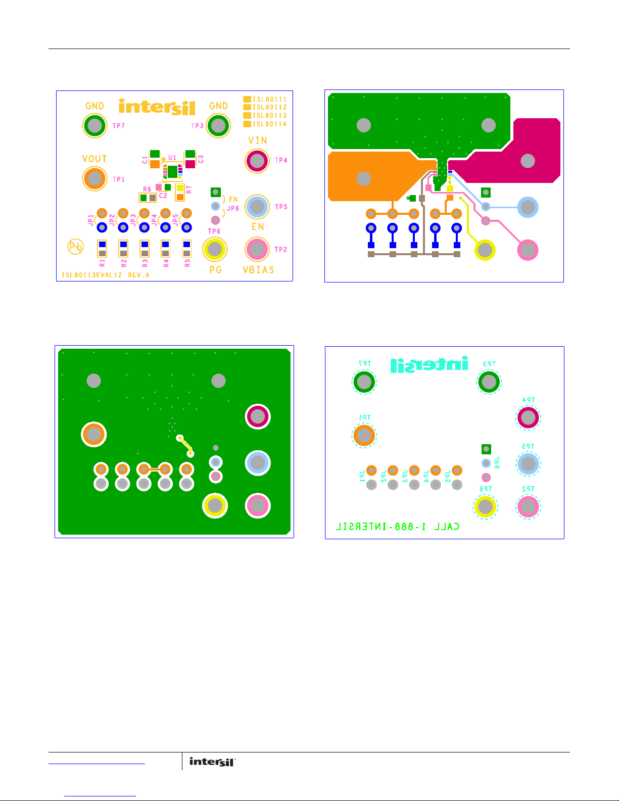
FIGURE 4. SILKSCREEN TOP FIGURE 5. TOP LAYER COMPONENT SIDE
User Guide 009
FIGURE 6. BOTTOM LAYER SOLDER SIDE
Submit Document Feedback
4
FIGURE 7. SILKSCREEN BOTTOM
UG009.0
October 30, 2014
Page 5
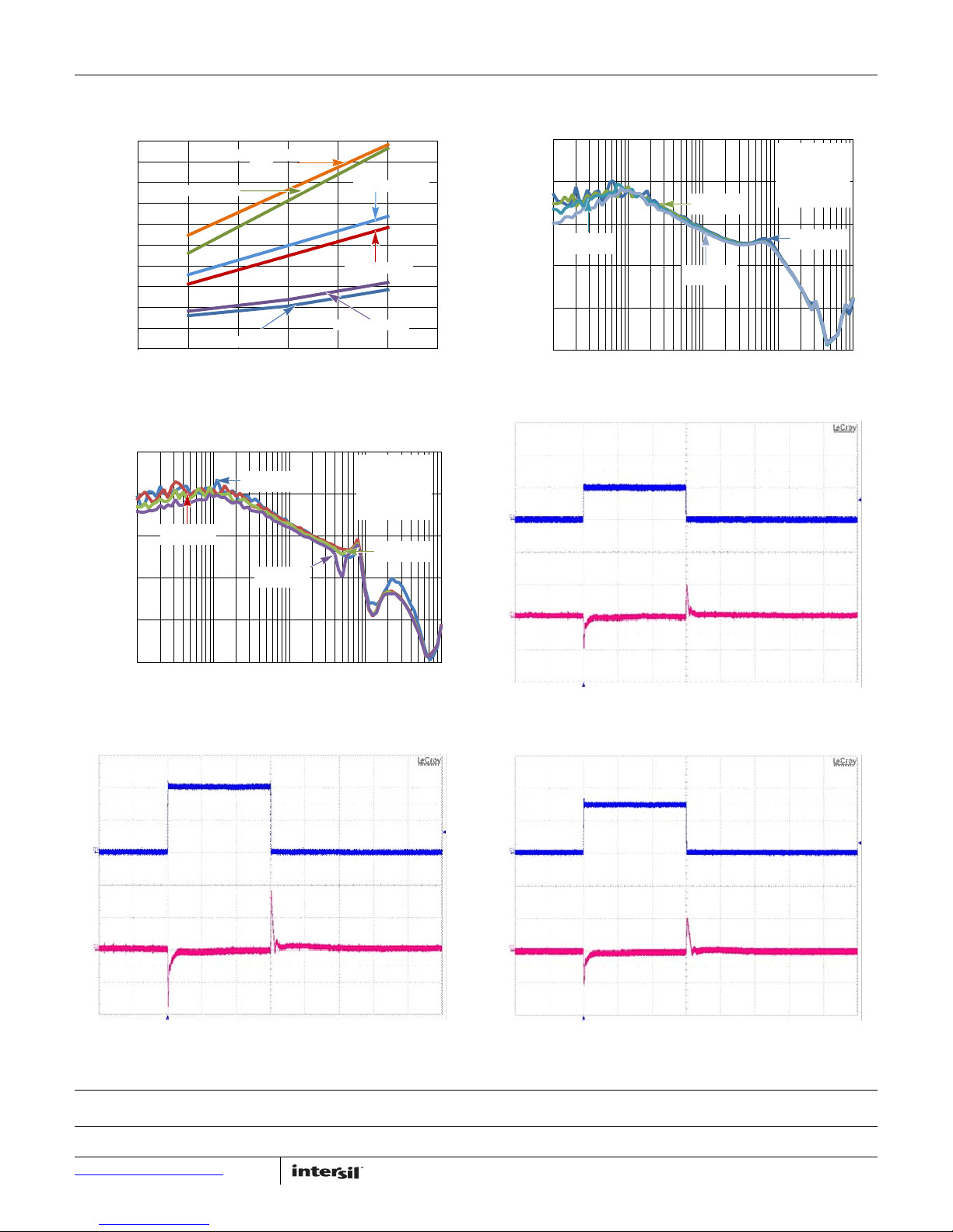
Typical Performance Curves
0
10
20
30
40
50
60
70
80
90
100
-40 25 125
TEMPERATURE (°C)
3A V
BIAS
= 3.3V
3A V
BIAS
= 5V
2A V
BIAS
= 5V
1A V
BIAS
= 3.3V
1A V
BIAS
= 5V
VIN DROPOUT VOLTAGE (mV)
2A V
BIAS
= 3.3V
0
20
40
60
80
100
100 1k 10k 100k 1M
PSRR (dB)
FREQUENCY (Hz)
I
OUT
= 2A
I
OUT
= 3A
I
OUT
= 0A
I
OUT
= 1A
BIAS = 5V
V
OUT
= 2.5V
V
IN
= 3.3V
C
OUT
= 10µF
0
20
40
60
80
100
100 1k 10k 100k 1M
PSRR (dB)
FREQUENCY (Hz)
I
OUT
= 0A
I
OUT
= 2A
BIAS = 3.3V
V
OUT
= 1.0V
V
IN
= 1.5V
C
OUT
= 10µF
I
OUT
= 3A
I
OUT
= 1A
V
OUT
(20mV/DIV)
I
OUT
= 1.1A
I
OUT
= 0.1A
TIME (20µs/DIV)
V
OUT
(20mV/DIV)
I
OUT
= 2.1A
I
OUT
= 0.1A
TIME (20µs/DIV)
V
OUT
(50mV/DIV)
I
OUT
= 3.1A
I
OUT
= 0.1A
TIME (20µs/DIV)
User Guide 009
FIGURE 8. DROPOUT vs V
FIGURE 10. V
PSRR vs LOAD CURRENT
VIN
BIAS
FIGURE 9. VIN PSRR vs LOAD CURRENT
FIGURE 11. 1A LOAD TRANSIENT RESPONSE
FIGURE 12. 2A LOAD TRANSIENT RESPONSE
Intersil Corporation reserves the right to make changes in circuit design, software and/or specifications at any time without notice. Accordingly, the reader is
cautioned to verify that the Application Note or Technical Brief is current before proceeding.
Submit Document Feedback
For information regarding Intersil Corporation and its products, see www.intersil.com
5
FIGURE 13. 3A LOAD TRANSIENT RESPONSE
UG009.0
October 30, 2014
 Loading...