intersil ISL80103 DATA SHEET
High Performance 2A and 3A LDOs
ISL80102, ISL80103
ISL80102, ISL80103
The ISL80102 and ISL80103 are low voltage,
high-current, single output LDOs specified for 2A and 3A
output current, respectively. These parts operate from
input voltages of 2.2V to 6V and are capable of providing
output voltages of 0.8V to 5V on the adjustable V
OUT
versions. Fixed output voltage options available in 0.8V,
1.2V, 1.5V, 1.8V, 2.5V, 3.3V and 5V. Other custom
voltage options availabl e upon request.
For applications that demand in-rush current less than
current limit, an external capacitor on the in-rush set pin
provides adjustment. The ENABLE feature allows the part
to be placed into a low quiescent current shutdown
mode. Sub-micron CMOS process is utilized for this
product family to deliver the best in class analog
performance and overall value.
These CMOS LDOs will consume significantly lower
quiescent current as a function of load over bipolar LDOs,
which translates into higher efficiency and the ability to
consider packages with smaller footprints. Quiescent
current is modestly compromised to enable a leading
class fast load transient response, and hence a lower
total AC regulation band for an LDO in this category .
Pin Configuration
ISL80102, ISL80103
(10 LD 3X3 DFN)
TOP VIEW
V
OUT
V
OUT
SENSE/ADJ
PG
GND
1
2
3
4
5
10
9
8
7
6
V
IN
V
IN
DNC
ENABLE
SS
Features
• 0.5% initial V
• Designed for 2.2V to 6V Input Supply
• ±1.8% Guaranteed V
Temperature Range from -40°C to +125°C
• 185mV Dropout @ 3A, 125mV Dropout @ 2A
• Fast Load Transient Response
• Rated Output Current Options of 2A and 3A
• Adjustable In-Rush Current Limiting
• Fixed and Adjustable V
• 65dB Typical PSRR
• Output Noise of 100µV
300kHz
•PG Feature
•900mV Enable Input Threshold
• Short-Circuit Current Protection
• 1A Peak Reverse Current
• Over-Temperature Shutdown
• Any Cap Stable with Minimum 10µF Ceramic
• Available in a 10 Ld DFN Package and soon to follow
TO220-5, TO263-5 and SOT223-5 (1A and 2A
versions)
• Pb-Free (RoHS Compliant)
Accuracy
OUT
Accuracy for Junction
OUT
Options Available
OUT
between 300Hz to
RMS
Applications*(see page 15)
• DSP, FPGA and µP Core Power Supplies
• Noise-Sensitive Instrumentation Systems
• Post Regulation of Switched Mode Power Supplies
• Industrial Systems
•Medical Equipment
• Telecommunications and Networking Equipment
•Servers
• Hard Disk Drives (HD/HDD)
September 30, 2009
FN6660.0
1
CAUTION: These devices are sensitive to electrostatic discharge; follow proper IC Handling Procedures.
1-888-INTERSIL or 1-888-468-3774
| Intersil (and design) is a regi s t ered trademark of Intersil Americas Inc.
All other trademarks mentioned are the property of their respective owners.
Copyright Intersil Americas Inc. 2009. All Rights Reserved
ISL80102, ISL80103
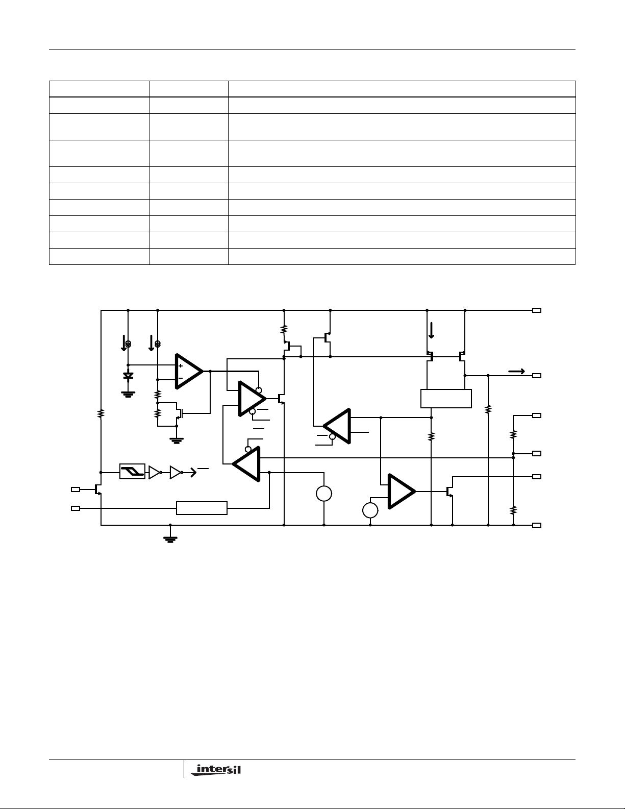
Pin Descriptions
PIN NUMBER PIN NAME DESCRIPTION
1, 2 V
OUT
Output voltage pin.
3 SENSE/ADJ Remote voltage sense for internally fixed V
V
.
OUT
4PGV
in regulation signal. Logic low defines when V
OUT
grounded if not used.
5GNDGND pin.
6 SS External cap controls in-rush current.
7ENABLE V
independent chip enable. TTL and CMOS compatible.
IN
8 DNC Do not connect this pin to ground or supply. Leave floating.
9, 10 V
IN
Input supply pin.
EPAD Must be soldered directly to GND plane
Block Diagram
options. ADJ pin for externally set
OUT
is not in regulation. Must be
OUT
VIN
EN
SS
10µA
R7
M7
10µA
R9
R8
ENEN
V TO I
+
-
IL/10,000
M3
-
+
LEVEL
SHIFT
R4
M1
POWER PMOS
IL
R1
M2
VOUT
SNS
R2
ADJ
PG
R3
GND
R4
M5
+
EN
EN
+
-
500mV
EN
+-+
-
M4
500mV
+
485mV
2
September 30, 2009
FN6660.0
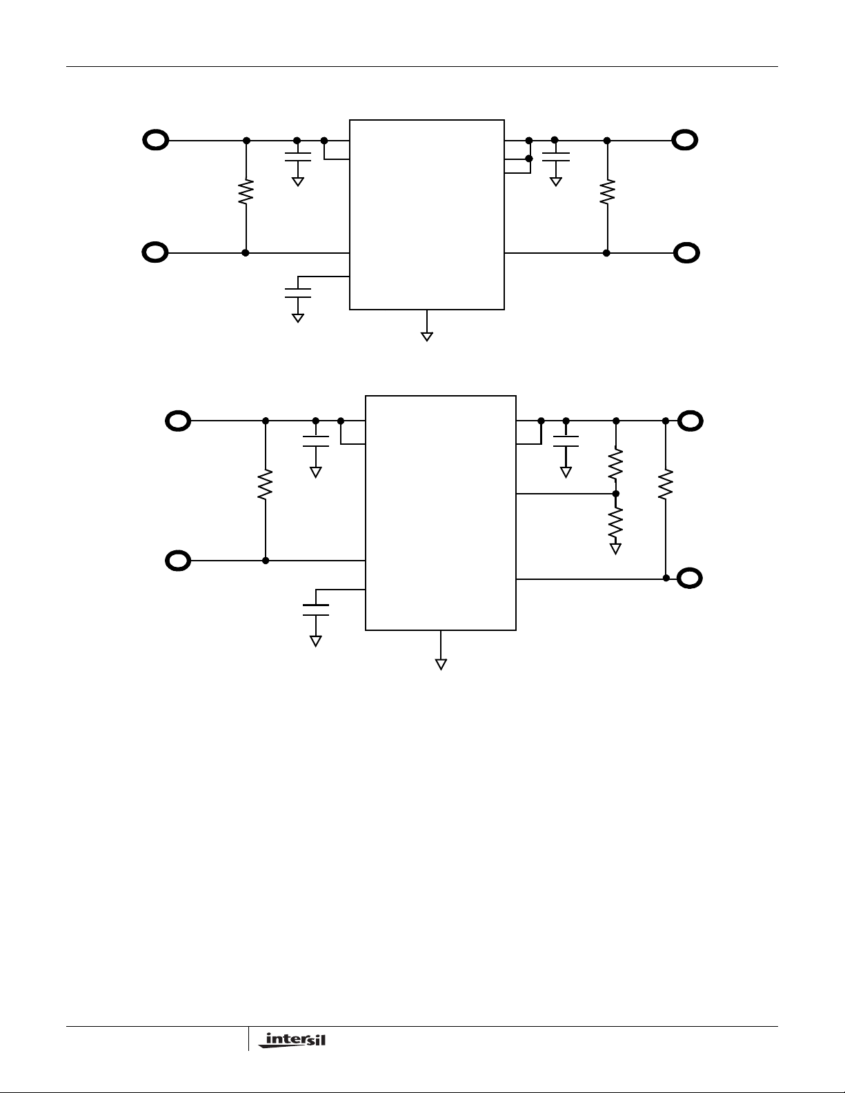
Typical Applications
ISL80102, ISL80103
2.5V ± 10% 1.8V ± 1.8%
10µF 10
10k
(*Note 12)
9
10
7
6
V
IN
V
IN
ENABLE
SS
ISL80102
ISL80103
GN D
5
FIXED
V
V
SENSE/ADJ
OUT
OUT
PG
1
2
3
4
µ
F
100k
FIGURE 1.
V
V
OUT
OUT
1
2
2.6k
100k
1k
10
9
V
IN
IN
ISL80102
ISL80103
SE
NSE/ADJ
V
2.5V ± 10% 1.8V ± 1.8%
10µF 10µF
10k
(*NOTE 12)
7
6
ENABLE
SS
FIGURE 2.
GND
5
JUSTABLE
AD
PG
4
3
September 30, 2009
FN6660.0
Ordering Information
ISL80102, ISL80103
PART NUMBER
ISL80102IRAJZ
(Notes 1, 3)
ISL80102IR08Z
(Notes 1, 3)
ISL80102IR12Z
(Notes 1, 3)
ISL80102IR15Z
(Notes 1, 3)
ISL80102IR18Z
(Notes 1, 3)
ISL80102IR25Z
(Notes 1, 3)
ISL80102IR33Z
(Notes 1, 3)
ISL80102IR50Z
(Notes 1, 3)
ISL80103IRAJZ
(Notes 1, 3)
ISL80103IR08Z
(Notes 1, 3)
ISL80103IR12Z
(Notes 1, 3)
ISL80103IR15Z
(Note 3)
ISL80103IR15Z-T
(Notes 2, 3)
ISL80103IR18Z
(Notes 1, 3)
ISL80103IR25Z
(Notes 1, 3)
ISL80103IR33Z
(Note 3)
ISL80103IR33Z-T
(Notes 2, 3)
ISL80103IR50Z
(Note 3)
ISL80103IR50Z-T
(Notes 2, 3)
NOTES:
1. Add “-T” or “-TK” suffix for tape and reel. Please refer to TB347
2. Please refer to TB347
3. These Intersil Pb-free plastic pac kaged products employ special Pb-free material sets, molding compounds/die attach
materials, and 100% matte tin plate plus anneal (e3 termination finish, which is RoHS compliant and compatible with both
SnPb and Pb-free soldering operations). Intersil Pb-free products are MSL classified at Pb-free peak reflow temperatures that
meet or exceed the Pb-free requirements of IPC/JEDEC J STD-020 .
4. For other output voltages, contact Intersil Marketing.
5. For Moisture Sensitivity Level (MSL), please see device information page for ISL80102,
MSL please see techbrief TB363
PART
MARKING
DZJA ADJ -40 to +125 10 Ld 3x3 DFN L10.3x3
DZKA 0.8V -40 to +125 10 Ld 3x3 DFN L10.3x3
DZLA 1.2V -40 to +125 10 Ld 3x3 DFN L10.3x3
DZMA 1.5V -40 to +125 10 Ld 3x3 DFN L10.3x3
DZNA 1.8V -40 to +125 10 Ld 3x3 DFN L10.3x3
DZPA 2.5V -40 to +125 10 Ld 3x3 DFN L10.3x3
DZRA 3.3V -40 to +125 10 Ld 3x3 DFN L10.3x3
DZSA 5.0V -40 to +125 10 Ld 3x3 DFN L10.3x3
DZAA ADJ -40 to +125 10 Ld 3x3 DFN L10.3x3
DZBA 0.8V -40 to +125 10 Ld 3x3 DFN L10.3x3
DZCA 1.2V -40 to +125 10 Ld 3x3 DFN L10.3x3
DZDA 1.5V -40 to +125 10 Ld 3x3 DFN L10.3x3
DZDA 1.5V -40 to +125 10 Ld 3x3 DFN
DZEA 1.8V -40 to +125 10 Ld 3x3 DFN L10.3x3
DZFA 2.5V -40 to +125 10 Ld 3x3 DFN L10.3x3
DZGA 3.3V -40 to +125 10 Ld 3x3 DFN L10.3x3
DZGA 3.3V -40 to +125 10 Ld 3x3 DFN
DZHA 5.0V -40 to +125 10 Ld 3x3 DFN L10.3x3
DZHA 5.0V -40 to +125 10 Ld 3x3 DFN
for details on reel specifications.
.
V
OUT
(Note 4)
VOLTAGE
TEMP. RANGE
(°C)
for details on reel specifications.
PACKAGE
(Pb-Free)
Tape and Reel
Tape and Reel
Tape and Reel
ISL80103. For more information on
PKG
DWG. #
L10.3x3
L10.3x3
L10.3x3
4
September 30, 2009
FN6660.0
ISL80102, ISL80103
Absolute Maximum Ratings (Note 8) Thermal Information
VIN relative to GND . . . . . . . . . . . . . . . . . . -0.3V to +6.5V
V
relative to GND . . . . . . . . . . . . . . . . . -0.3V to +6.5V
OUT
PG, ENABLE, SENSE/ADJ, SS
Relative to GND. . . . . . . . . . . . . . . . . . . . -0.3V to +6.5V
Recommended Operating Conditions
Junction Temperature Range (TJ) . . . . . . . -40°C to +125°C
VIN relative to GND . . . . . . . . . . . . . . . . . . . . . 2.2V to 6V
V
range . . . . . . . . . . . . . . . . . . . . . . . . . .800mV to 5V
OUT
PG, ENABLE, SENSE/ADJ, SS relative to GND . . . . .0V to 6V
PG sink current . . . . . . . . . . . . . . . . . . . . . . . . . . . . 10mA
CAUTION: Do not operate at or near the maximum ratings listed for extended periods of time. Exposure to such conditions may adversely impact
product reliability and result in failures not covered by warranty.
NOTES:
is measured in free air with the component mounted on a high effective th ermal conductivity test board with “direct attach”
6. θ
JA
features. See Tech Brief TB379.
7. For θ
8. ABS max voltage rating is defined as the voltage applied for a lifetime average duty cycle above 6V of 1%.
, the “case temp” location is the center of the exposed metal pad on the package underside.
JC
Thermal Resistance (Typical) θ
(°C/W) θJC (°C/W)
JA
10 Ld 3x3 DFN Package (Notes 6, 7) 45 4
Maximum Junction Temperature (Plastic Package). . . +150°C
Storage Temperature Range. . . . . . . . . . . - 65°C to +150°C
Pb-Free Reflow Profile . . . . . . . . . . . . . . . . . .see link below
http://www.intersil.com/pbfree/Pb-FreeReflow.asp
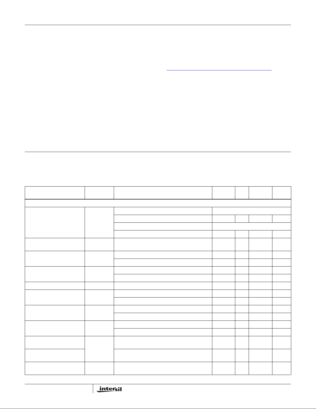
Electrical Specifications Unless otherwise noted, all parameters are established over the following specified
conditions: V
Applications must follow thermal guidelines of the package to determine worst case junction
temperature. Please refer to “Application Section” on page 7 and Tech Brief TB379.
Boldface limits apply over the operating temperature range, -40°C to +125°C. Pulse
load techniques used by ATE to ensure T
PARAMETER SYMBOL TEST CONDITIONS
DC CHARACTERISTICS
DC Output Voltage
Accuracy
Feedback Pin (ADJ option
only)
DC Input Line Regulation ΔV
DC Output Load Regulation ΔV
V
V
OUT
OUT
OUT
FB
T
/ΔVINV
/ΔI
OU
Feedback Input Current V
Ground Pin Current I
Ground Pin Current in
I
SHDN
Q
Shutdown
Dropout Voltage (Note 10) V
Output Short Circuit
DO
ISC V
Current (3A Version)
Output Short Circuit
Current (2A Version)
Thermal Shutdown
Temperature
TSD
= V
IN
V
Options: 0.8V, 1.2V, 1.5V and 1.8V
OUT
2.2V < V
Options: 2.5V, 3.3V and 5.0V
V
OUT
+ 0.4V < V
V
OUT
2.2V < V
+ 0.4V < V
OUT
+ 0.4V < V
V
OUT
0A < I
LOAD
0A < I
LOAD
= 0.5V 0.01 1 µA
ADJ
I
= 0A, 2.2V < V
LOAD
= 3A, 2.2V < V
I
LOAD
ENABLE Pin = 0.2V, V
ENABLE Pin = 0.2V, V
I
= 3A, V
LOAD
= 2A, V
I
LOAD
= 0V, V
OUT
V
= 0V, V
OUT
V
+ 0.4V < V
OUT
+ 0.4V, V
OUT
< 3.6V; 0A < I
IN
IN
< 6V, 0A < I
IN
IN
IN
< 6V; 0A < I
< 3.6V, V
< 6V, V
= 1.8V, C
OUT
= TA defines established limits.
J
< 3A -1.8 0.5 1.8 %
LOAD
LOAD
< 3A 491 500 509 mV
LOAD
= 1.8V 0.1 0.4 %
OUT
= 2.5V 0.1 0.8 %
OUT
IN
= C
= 10µF, TJ = +25°C, IL = 0A
OUT
MIN
(Note 9) TYP
MAX
(Note 9) UNITS
< 3A -1.8 0.5 -1.8 %
< 3A, All voltage options -0.8 %
< 2A, All voltage options -0.6 %
< 6V 7.5 9 mA
IN
< 6V 8.5 12 mA
IN
= 5V 0.4 µA
IN
= 6V 3.3 16 µA
IN
= 2.5V 120 185 mV
OUT
= 2.5V 81 125 mV
OUT
+ 0.4V < V
OUT
+ 0.4V < V
OUT
< 6V 160 °C
IN
< 6V 5.0 A
IN
< 6V 2.8 A
IN
5
September 30, 2009
FN6660.0
 Loading...